Article

Advanced Single-Phase Non-Isolated Microinverter with Time-Sharing Maximum Power Point Tracking Control Strategy

Faculty of Engineering and Applied Sciences, Cranfield University, Bedford MK43 0AL, UK
*
Author to whom correspondence should be addressed.
Energies 2025, 18(18), 4925; https://doi.org/10.3390/en18184925
Submission received: 29 July 2025 / Revised: 1 September 2025 / Accepted: 10 September 2025 / Published: 16 September 2025
(This article belongs to the Special Issue Advanced Control Strategies for Photovoltaic Energy Systems)

Abstract

Partial shading poses a significant challenge to photovoltaic (PV) systems by degrading power output and overall efficiency, especially under non-uniform irradiance conditions. This paper proposes an advanced time-sharing maximum power point tracking (MPPT) control strategy implemented through a non-isolated single-phase multi-input microinverter architecture. The system enables individual power regulation for multiple PV modules while preserving their voltage–current (V–I) characteristics and eliminating the need for additional active switches. Building on the concept of distributed MPPT (DMPPT), a flexible full power processing (FPP) framework is introduced, wherein a single MPPT controller sequentially optimizes each module’s output. By leveraging the slow-varying nature of PV characteristics, the proposed algorithm updates control parameters every half-cycle of the AC output, significantly enhancing controller utilization and reducing system complexity and cost. The control strategy is validated through detailed simulations and experimental testing under dynamic partial shading scenarios. Results confirm that the proposed system maximizes power extraction, maintains voltage stability, and offers improved thermal performance, particularly through the integration of GaN power devices. Overall, the method presents a robust, cost-effective, and scalable solution for next-generation PV systems operating in variable environmental conditions.

1. Introduction

Photovoltaic (PV) generation systems (PGSs) are increasingly prominent within the global renewable energy landscape [1]. In a conventional PGS, individual PV cells are connected in series to form a PV module. Multiple modules are then connected in series to form a PV string, generating a high direct current (DC) voltage [2]. Several PV strings are finally connected in parallel to form a PV array. While these systems generally achieve high power conversion efficiency, their performance can significantly degrade under non-ideal operating conditions. A key area of concern is the development and refinement of maximum power point tracking (MPPT) technologies [3], which are crucial for enhancing the overall energy yield of PV systems. However, conventional centralized maximum power point tracking (CMPPT) techniques suffer from several drawbacks, primarily due to mismatches among system components [4]. These mismatches arising from partial shading, soiling, temperature gradients, aging, or manufacturing inconsistencies can occur both between modules in a PV string and within submodules of a single module [5,6,7]. This paper specifically addresses the mismatch at the module level, which not only leads to energy loss but may also cause long-term physical damage such as hotspots [8], accelerated module degradation [9], overcurrent [10], and nuisance tripping [11]. The fundamental limitation lies in the series-connected architecture, where the performance of the weakest cell dictates the performance of the entire string. To mitigate the impact of hotspots, bypass diodes are typically installed within PV module junction boxes. For instance, a common approach is to protect every group of 18–22 PV cells with a single bypass diode. However, this solution introduces the issue of multiple power peaks on the I–V and P–V curves, including one global maximum power point (GMPP) and several local maximum power points (LMPPs). These multiple peaks not only complicate GMPP tracking but are also associated with recombination-related losses within the solar cell, as shown by Abudulimu et al. [12], who demonstrated through bias-dependent quantum efficiency that distinct recombination pathways significantly impact carrier collection efficiency and, in turn, the P–V curve profile.
Research by Ncir et al. [13] proposed a differential evolution algorithm-based feed-forward neural network (DE-FFNN). Although the proposed time-sharing MPPT strategy offers improved power extraction and cost efficiency, it has limitations. The sequential control nature may introduce slight delays in dynamic response compared with fully parallel DMPPT systems. Figure 1a illustrates the effect of partial shading on a PV module composed of three submodules, each receiving different irradiance levels. This mismatch activates the bypass diodes in the shaded submodules, resulting in the multi-peak behavior shown in the I–V and P–V curves in Figure 1b. While global MPPT (GMPPT) algorithms are employed to address this issue, they cannot ensure that each module or submodule consistently operates at its individual GMPP under all partial shading scenarios. As seen in Figure 1b, although the system is regulated to the global MPP at point G, significant power loss persists due to bypassed submodules, as indicated by shaded regions A4, A5, and A6. To address these challenges, distributed maximum power point tracking (DMPPT) architectures have been proposed [14], and they have garnered increasing attention in both academic research and industrial applications [15]. In contrast with centralized and string-level MPPT configurations, panel-level MPPT systems minimize mismatch losses by allowing each panel to operate at its own MPP, thereby maximizing energy extraction. DMPPT systems deploy individual MPPT circuits for each panel or small group of panels, enhancing overall system resilience to shading and non-uniform conditions. There are two main approaches to DMPPT: differential power processing (DPP) [16,17,18] and full power processing (FPP) [19,20,21,22].
Research by Madeti [23] emphasized the need for an efficient energy balance in the PV system and how it impacts the overall system efficiency. A fundamental distinction between the two DMPPT architectures lies in the configuration of their PV cell groups. In differential power processing (DPP), the cell units are connected in series, whereas in full power processing (FPP), they operate independently. The DPP structure enables high MPPT granularity, reaching the submodule or even cell level, which enhances its ability to effectively mitigate mismatch losses [20]. However, this fine-grained control introduces considerable complexity, requiring multiple control loops, extensive converter coupling, and a larger number of devices. A detailed comparison of the DPP and FPP architectures is presented in Table 1, highlighting key differences in coupling levels, converter requirements, communication needs, and system scalability.
Given the advantages of FPP in terms of simplified structure and reduced cost, this paper adopts the FPP framework as its foundation. Nevertheless, one major drawback of FPP systems, particularly those employing subpanel-level MPPT, is the increased cost associated with dedicating a separate MPPT controller to each PV cell string. To address this issue, a time-sharing MPPT controller is proposed in this work, allowing a single MPPT unit to sequentially track the maximum power point (MPP) of each PV module during discrete time intervals [21,22,24]. In addition, a self-adaptively adjusted enable signal is integrated into the control scheme, which intelligently activates MPPT tracking only when environmental changes are detected. This enhancement enables faster and more efficient MPP tracking under dynamic conditions while minimizing system cost and complexity. To build upon earlier work involving a novel single-phase non-isolated dual-input microinverter (MI) with a common ground, this study introduces an advanced time-sharing MPPT control strategy. The key contributions of this paper are summarized as follows:
  • This work addresses the challenge of performing MPPT for multiple PV panels with distinct I–V characteristics using a single shared microinverter, maintaining performance without degradation.
  • It eliminates the need for additional active switches by integrating a multi-input boost converter directly into an H-bridge structure, reducing cost and complexity.
  • The proposed control strategy leverages the slow-varying nature of PV panel characteristics, enabling efficient low speed control without requiring high-frequency updates.
  • A time-shared MPPT scheme is introduced, updating the tracking and modulation variables of each PV module once every half-cycle of the AC output, allowing coordinated operation across multiple inputs.
This paper is structured as follows: Section 1 introduces the concept of subpanel-level MPPT control and outlines the motivation for a time-sharing approach. Section 2 describes the proposed microinverter topology and its operational principles, including the integration of the time-sharing MPPT control strategy. Section 3 presents a simulation-based evaluation of the system under various PV source conditions. Section 4 discusses the experimental results that validate the proposed topology and control approach. The final section concludes this paper with key findings and potential directions for future research.

2. Proposed Microinverter Topology and Its Operation

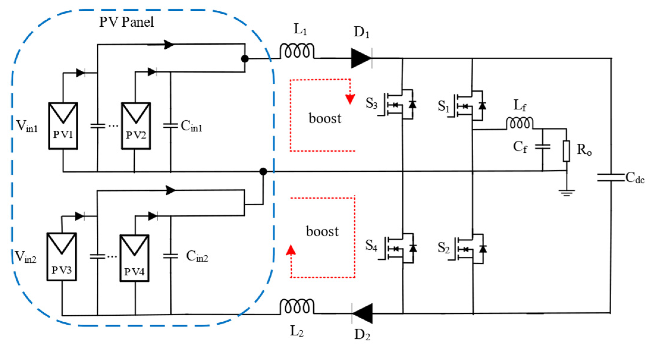
Figure 2 presents the proposed non-isolated multi-input microinverter (MI) featuring an active power decoupling function. The topology adopts a vertically symmetrical structure consisting of four active power switches (S1–S4) and two diodes (D1 and D2), which prevent reverse current from flowing back into the PV sources. Each PV input is supported by a parasitic capacitor (Cin1 and Cin2) to stabilize voltage and ensure smooth power transfer, especially under partial shading conditions. In Figure 2, the blue dotted line encloses the PV panel block, grouping PV1–PV4 together with their filter capacitors. This enclosure highlights the common midpoint connection of the PV sources to the ac ground, which stabilizes the PV terminal voltages and effectively suppresses high-frequency leakage currents. Meanwhile, the red dotted boxes labeled “boost” indicate the two boost subcircuits formed by inductors L1 and L2 and diodes D1 and D2. These paths are responsible for stepping up the PV voltages and transferring energy to the dc-link capacitor Cdc, which subsequently feeds the H-bridge stage for ac output generation. Hence, the blue dotted line represents the leakage current suppression mechanism, while the red dotted boxes illustrate the dual-boost energy transfer loops. The configuration integrates two boost converters for the respective PV inputs, which are then merged and processed through a shared H-bridge inverter stage. The AC output is connected to the grid via a low-pass LC filter to suppress high-frequency switching noise and deliver a clean sinusoidal waveform. Key advantages of this topology include the following:
  • A reduced number of power switches of only four switches is required to interface four PV sources.
  • Built-in active power decoupling capability to enhance power quality.
  • Elimination of leakage current due to the common ground between the AC and DC sides.
  • Low current stress on switches and diodes, as they handle only the input current from each PV source.
A comparative evaluation is provided in Section 5, highlighting the performance of the proposed MI in terms of component count, voltage gain, leakage current suppression, and overall conversion efficiency.

2.1. Operation and Power Loss Analysis

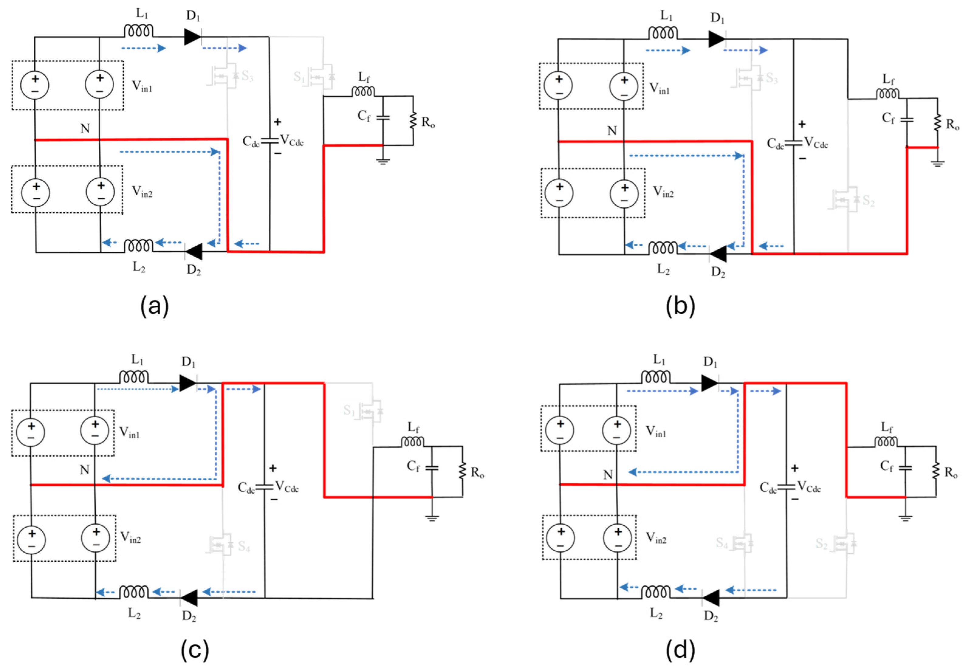
The proposed microinverter operates in a dual-boost mode, utilizing four independent PV modules as its input sources. By adjusting the switching states of the H-bridge, the system can generate four distinct configurations: active-1 (01), active-2 (10), null-1 (00), and null-2 (11). The binary values indicate the control signals for switches S1 and S3, with S2 and S4 functioning as their logical complements. Each switching state results in a different circuit behavior, as illustrated in Figure 3, where the blue arrows indicate the instantaneous current flow directions in each operating state of the inverter, showing how energy is transferred between the PV sources, inductors, switches, and the dc-link capacitor/output. The red lines highlight the active conduction paths formed when certain switches and diodes are conducting, thereby defining the voltage loops responsible for either charging the inductors during the boost phase or discharging them to deliver energy to the dc-link capacitor and load. Together, the blue arrows and red lines clearly illustrate the dynamic behavior of the proposed microinverter across its different switching states.
A pulse-width modulation (PWM) approach is applied in conjunction with a time-sharing MPPT algorithm to manage the H-bridge control. The sequence of states during a switching cycle depends on the polarity of the output current. During the positive half-cycle, the transitions follow the sequence (00, 10, 11), and during the negative half-cycle, the sequence becomes (00, 01,11). In the positive half-cycle, the operation of the circuit can be understood by referring to Figure 3a,b. During these states, input voltage Vin2 charges inductor L2 through switch S4, while L1 discharges (non-active) either into the DC-link capacitor Cdc (in the null state) or into the filter capacitor Cf (in the active state). Later, in Figure 3d (corresponding to the null-2 state), Vin1 charges (Active) L1 via S3, and L2 discharges into Cdc. Similar operating conditions occur during the negative half-cycle for Figure 3c, with the switching roles of L1 and L2 reversed. These operational details are summarized in Table 2 based on the states and fundamental half-cycle (FHC).
To accurately model system behavior, average inductor currents during the positive and negative cycles are labeled as ILx+ and ILx, respectively, where x = 1, 2. The average current through the DC-link capacitor is Ic, while io represents the inverter’s output current. Using the volt-second balance principle, the inductor dynamics across a full switching period Ts are governed by Equations (1) and (2):
V i n 1 d 3 T s + V i n 1 V C d c d L 1 T s = 0
V i n 2 d 4 T s + V i n 2 V C d c d L 2 T s = 0
where V C d c represent DC-link voltage, parameters d 3 and d 4 represent the time durations for switches S 3 and S 4 . The corresponding discharging intervals L1 and L2 must satisfy dL1 ≤ 1 − d3 and dL2 ≤ 1 − d4, representing the discharging duty ratios of the two inductors. These relationships depend on whether the inductors operate in discontinuous conduction mode (DCM) or continuous conduction mode (CCM). During the positive half-cycle, parameter d3 represents the duration of the null-2 state, while d4 covers the combined interval of the null-1 and active-1 states. Under sinusoidal PWM (SPWM), these duty ratios typically satisfy d3(t) < 0.5 and d4(t) = 1 − d3(t) > 0.5, indicating that inductor L2 is responsible for boosting the DC-link voltage. Consequently, Vdc exceeds twice the PV input voltage: VCdc > 2Vin. However, like in conventional SPWM-based inverters, the resulting DC-link voltage varies with time. To maintain stable operation, Vdc must remain greater than both 2Vin1 and 2Vin2. Under these conditions, L1 operates in DCM since its discharge duty dL1 remains less than d3(t), and their combined value stays below unity. In contrast, L2 may operate in either DCM or CCM depending on its instantaneous current ripple and average current. The current ripple of L2 is expressed by Equation (3).
i L 2 t = V i n 2 T s 2 L 2 d 4 ( t )
Losses in the system stem from inductor resistance, diode conduction, capacitor ESR, and MOSFET switching behavior. Assuming each inductor has parasitic resistance r L , the conduction loss associated with diode D1 can be calculated using the following expressions:
P L = 1 2 I L 2 + 2 r L + 1 2 I L 2 2
P d 1 = 1 2 ( I L 1 + + I L 1 ) V F
P c d c = r c f 1 0 1 2 f 1 I L 1 + 2 M d c 1 + i o I L 1 + 2 d 1 M d c 1 + I L 1 + 2 1 d 1 d t + 1 2 f 1 1 f 1 I L 1 2 ( 1 M d c 2 ) + I L 1 2 d 1 + i o I L 1 2 ( M d c 2 d 1 ) d t
where V F represents the forward voltage, with no significant contribution to the reverse recovery loss by diode D1. During the positive FHC, inductor L1 operates in DCM, conducting only a small current L1+ for a brief period. Consequently, the reverse current through D1, which is in series with L1, remains minimal. In the negative FHC, however, L1 transitions to CCM, resulting in D1 conducting continuously without inducing reverse recovery loss. Subsequent loss analysis is performed for the DC-link capacitor Cdc and the four H-bridge switches S1–S4. Starting with Cdc, its current expressions are derived from Table 2 to calculate power loss across its equivalent series resistance rc. The resulting expression is given by Equation (7). This expression can be simplified by neglecting the contributions of IL1+ and IL2, which are significantly smaller than IL1 and IL2+. The simplified form is ultimately presented as Equation (7).
P c d c = r c I L 2 + 2 1 M d c 1 2 M a c π + r c 4 V c d c 2 M a c 3 3 π R o 2
The conduction losses for S1–S4 due to respective ON-resistance R o n , is given by Equation (8), while the overall switching losses is given by Equation (9).
P c o n = I s x r m s 2 R o n
P s w x = 1 2 T s I s x V c d c ( t r + t f )
where 1/Ts is their common switching frequency, which, if raised, results in higher switching losses and worse efficiency, and tr and tf are the turn-ON turn-OFF timings of each switch. The total power loss (PLoss) can be calculated by summing these individual losses, as written in Equation (10). The efficiency (η) of the microinverter can be determined using Equation (11).
P l o s s = P c o n d   I n d u c t o r + P c o n d   D i o d + P c o n d   M O S + P s w M O S
η = V o I o P L o s s + V o I o
Finally, to determine the optimal operating point that maximizes the efficiency of the microinverter, a differential calculation of the efficiency (η) to the output voltage (Vo) can be performed. This can be expressed as Equation (12). By setting this differential equation to zero and solving for Vo, the value of the output voltage that corresponds to the maximum efficiency point of the microinverter within its OPR can be found.
d η d V O = ( P L o s s + V o I o ) . d d V O   ( V o I o ) ( P L o s s + V o I o ) 2   V o I o .     d d V o ( P L o s s + V o I o ) ( P L o s s + V o I o ) 2

2.2. MI Time-Sharing Algorithm and MPPT Control Strategy

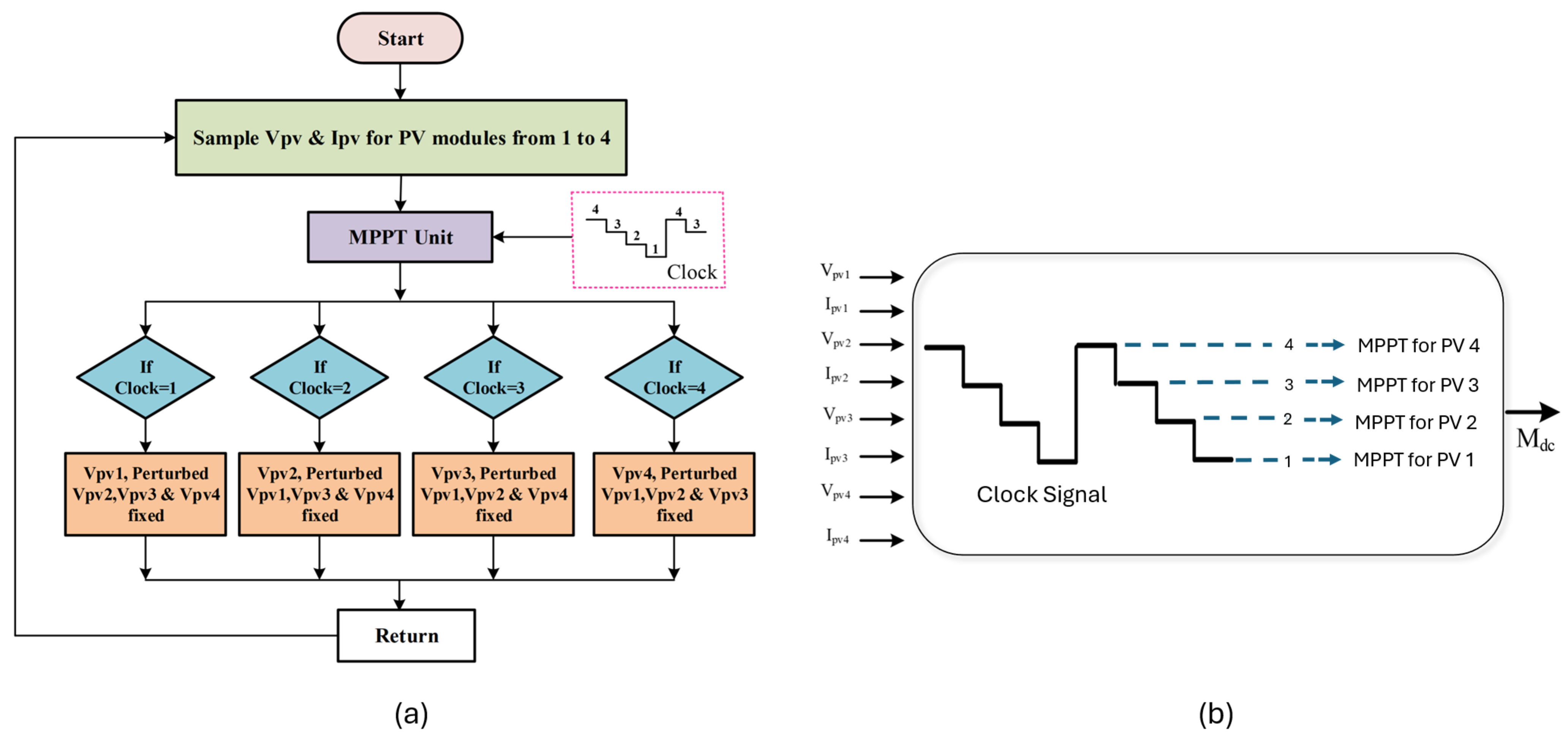
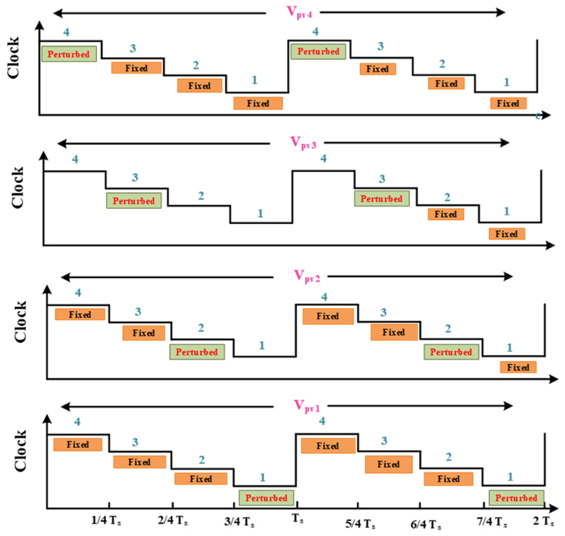
This paper proposes a cost-effective and scalable time-sharing MPPT (TS-MPPT) algorithm, the flow of which is depicted in Figure 4a. Traditional DMPPT designs often dedicate a full MPPT microcontroller to each module [8], which results in bulky hardware and increased demand for auxiliary power and interface circuitry. In contrast, the proposed TS-MPPT scheme operates with only a single MPPT controller that sequentially manages multiple PV modules by dividing the tracking process into discrete time intervals. As shown in Figure 4b, the controller is governed by a time-based clock signal that designates which PV module undergoes MPPT during each interval. The red dotted box in Figure 4a highlights the time-sharing clock signal, which sequentially allocates the MPPT operation among the PV modules. The blue dotted lines in Figure 4b represent the assignment of the MPPT algorithm to each PV module, controlled by the clock signal. Each clock level corresponds to one PV source, ensuring that the perturb and observe (P&O) algorithm is executed individually for one PV module while the others remain fixed.
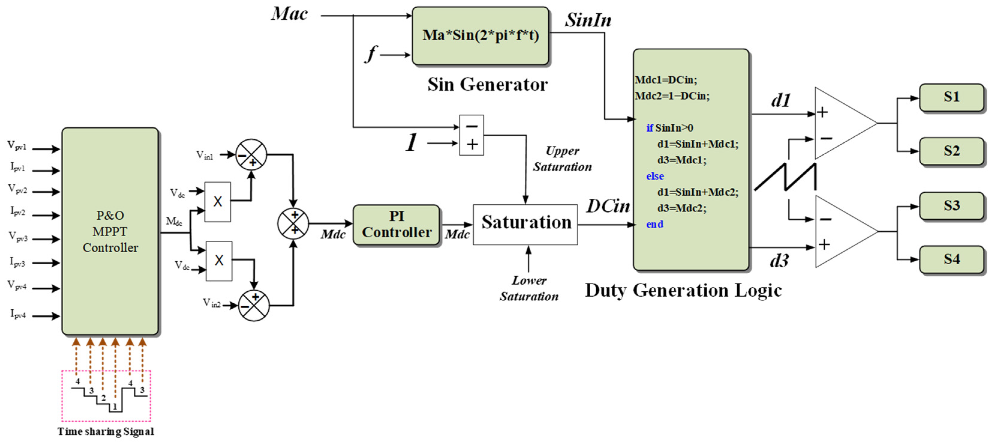
The control block of the TS-MPPT is presented in Figure 5. In this figure, the red dotted box highlights the time-sharing clock signal, which allocates the MPPT operation sequentially among the PV modules. The TS-MPPT exploits the relatively slow variation in solar irradiance compared with the high-speed operation of modern controllers. This allows a single MPPT unit to track the maximum power point (MPP) of one module at a time without compromising performance. During each time slice, the system samples voltage and current values for all modules. The MPPT algorithm then perturbs the active module while holding the others at their previously tracked MPP voltages. A decision mechanism evaluates whether the system has reached a steady state using preset thresholds for voltage (M) and current (∆I). If the perturbation results in minimal variation within these thresholds, the current module is deemed to have reached its MPP, and the controller shifts to the next module. Otherwise, the same module continues to be tracked.
Figure 6 illustrates how clock signals are distributed across PV modules 1 through 4. Each module alternates between two states: perturbation (active MPPT) and fixed (voltage-following). When, for example, the clock signal is set to “4”, the MPPT algorithm actively perturbs PV module 4 to track its MPP, while modules 1–3 are held at the voltage reference derived from module 4. Once module 4’s MPP is achieved, the clock updates to “3”, initiating MPPT for module 3 while the others follow. This sequence continues in descending order through modules 2 and 1, as indicated by the flowchart in Figure 4a. When a module not currently being tracked experiences a significant change in irradiance (∆I exceeds threshold), it will be prioritized in the next cycle. Unlike conventional MPPT schemes, this technique allows multiple PV panels to share a single MPPT controller without sacrificing performance. It is particularly useful for modular PV systems where several panels are connected to a shared microinverter. The method effectively balances energy extraction, simplifies the control architecture, and minimizes the number of sensors and controllers needed. The time-sharing control diagram is detailed in Figure 4b.
The overall control system manages a non-isolated multi-input microinverter using the perturb and observe (P&O) algorithm within a TS-MPPT framework. Voltage and current data from the four PV modules (Vpv1,Vpv2,Vpv3,Vpv4 and Ipv1,Ipv2,Ipv3,Ipv4) are processed by a central MPPT controller that operates on a shared schedule. The output of the MPPT algorithm generates a modulation index (Mdc), used for voltage regulation and switching control. To maintain stable voltage, the system compares the PV input voltages with reference values. Any deviations are corrected using a PI controller, which adjusts the modulation index accordingly. A saturation block restricts this output to avoid overshoot and maintain system stability. The final stage of the control sequence involves PWM signal generation. A sinusoidal modulator (Mac) creates a reference waveform, which feeds into the duty generation logic that calculates the required duty cycles (d1, d2, d3) for controlling the four switches (S1–S4). These duty cycles ensure synchronized operation of the dual-boost converter and efficient energy delivery to the grid or load. The combination of time-sharing MPPT, PI-based voltage control, and sinusoidal PWM modulation significantly enhances energy harvesting performance while minimizing hardware requirements and control complexity. The proposed method is also extendable, provided that timing coordination and tracking stability are carefully managed in dynamically changing environmental conditions.

3. Simulation Evaluation with PV Sources

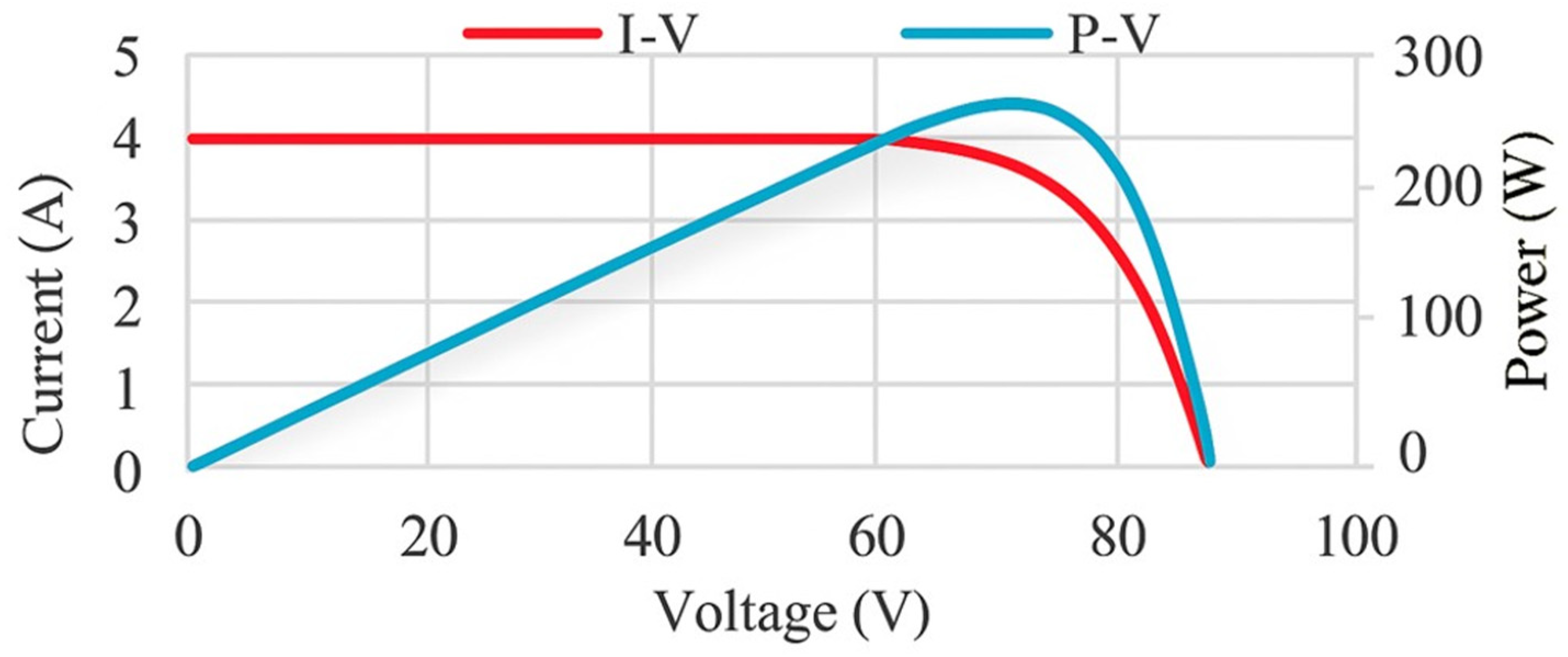
The proposed multi-input microinverter was simulated in MATLAB/Simulink to assess its effectiveness for photovoltaic (PV) applications. The simulation parameters for the design are outlined in Table 3. The simulation setup consisted of four PV modules, each connected in parallel with a 3.3 mF capacitor to filter out high-frequency noise and stabilize the voltage input. All PV modules were configured with identical electrical characteristics to ensure consistent performance across inputs. Figure 7 displays the simulated current–voltage (I–V) and power–voltage (P–V) curves for a single PV module. The maximum power point (MPP) is clearly identifiable at the peak of the P–V curve, validating the expected behavior of the PV source model. In the control system, the inverter tracks the MPP by dynamically adjusting the modulation indices Mdc1 and Mdc2. These indices directly influence the average current through inductors L1 and L2, allowing precise control of power flow from each input source. This enables efficient extraction of power even under varying irradiance conditions when integrated with the time-sharing MPPT algorithm described earlier.

3.1. Fixed Irradiance Conditions

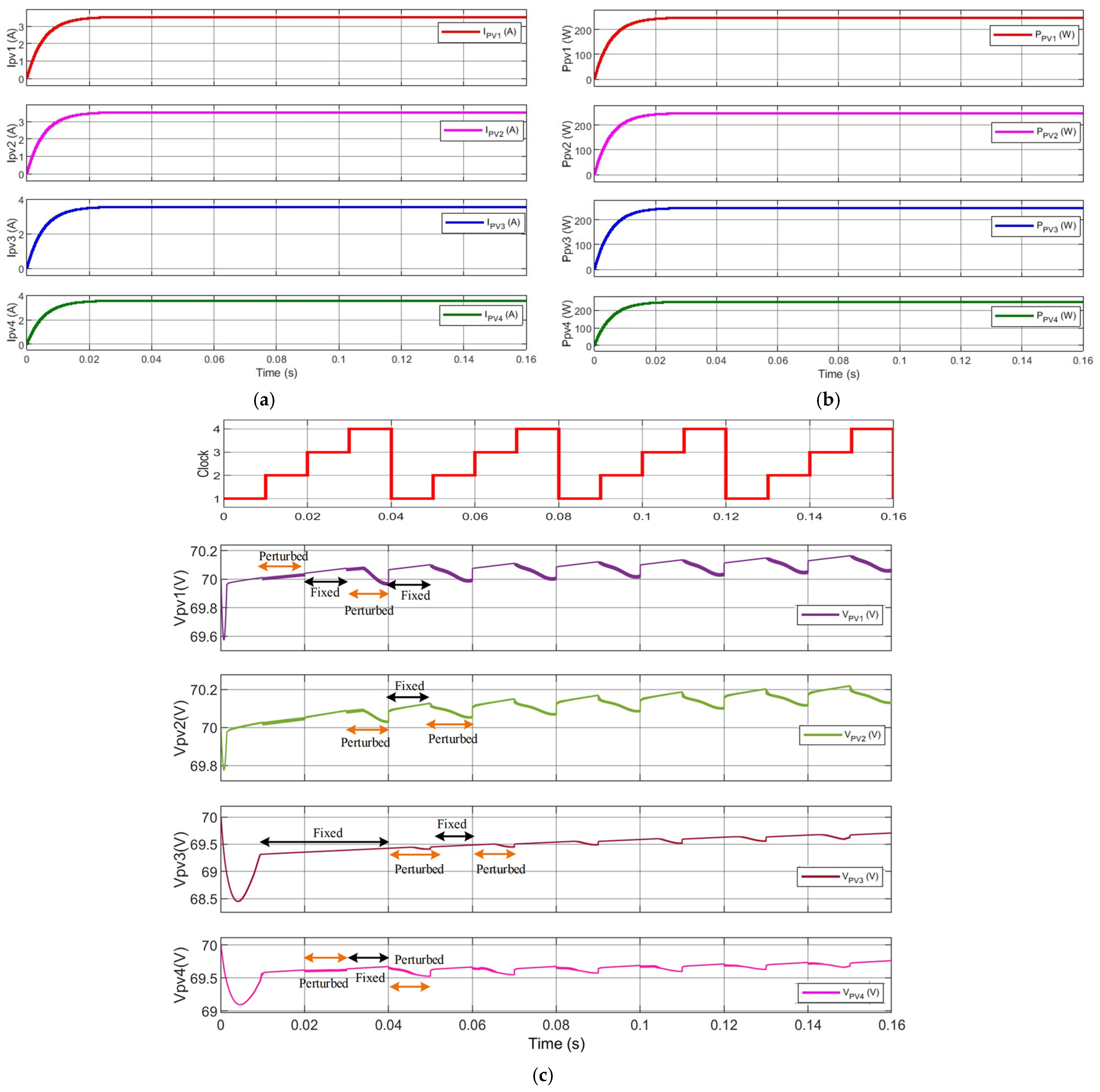
To validate the performance of the proposed control system, a simulation was conducted under fixed irradiance conditions. The scenario involves four PV modules operating under mismatch conditions, with their maximum power point (MPP) currents set to 3.76 A, 3.41 A, 3.63 A, and 3.55 A, respectively. The system incorporates both the time-sharing MPPT algorithm and the microinverter’s current–voltage regulation capabilities. The simulated results are presented in Figure 8. The corresponding current and power waveforms for each module are presented in Figure 8a,b. Figure 8c illustrates the voltage profiles of all PV modules in relation to the enable clock signal. Initially, when the clock signal is “1”, MPPT is enabled for PV1, while PV2 follows PV1’s voltage reference. At 0.01 s, the clock advances to “2”, activating MPPT for PV2 and holding PV1’s voltage constant. PV3 and PV4 remain in fixed-voltage mode. At 0.03 s, the clock shifts to “3”, initiating MPP tracking for PV3 while PV4 enters voltage-following mode and the remaining modules remain fixed. By 0.04 s, MPPT is enabled for PV4, and the other modules continue tracking the reference voltage derived from PV3. The process successfully brings all PV modules to their MPPs by approximately 0.042 s. A new clock cycle begins at 0.045 s to maintain MPP operation under stable conditions. As observed, all PV modules rapidly converge toward their maximum output within the first 0.05 s, confirming the effectiveness of the time-sharing strategy in coordinating MPP tracking.

3.2. Dynamic Irradiance Conditions

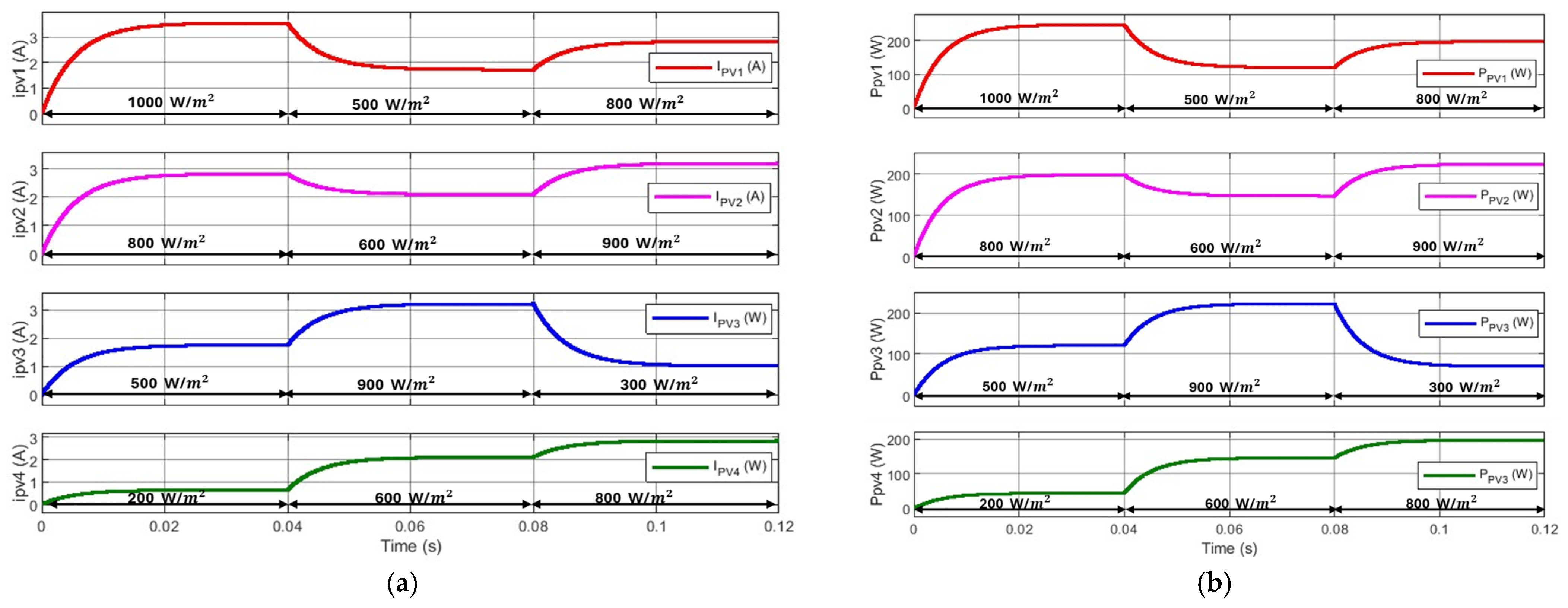
The robustness of the proposed time-sharing MPPT control strategy evaluation in a dynamic irradiance scenario was simulated. In this simulation setup, the PV modules were subjected to step changes in irradiance at different time intervals, as summarized in Figure 9. During the interval from 0 to 0.04 s, PV1 decreases from 1000 to 500 W/m2, PV2 reduces from 800 to 600 W/m2, while PV3 increases from 500 to 900 W/m2. Between 0.04 and 0.08 s, PV1 rises from 200 to 600 W/m2, PV2 remains within the range of 800 to 600 W/m2, and PV3 is maintained at 500 to 900 W/m2. From 0.08 to 0.12 s, PV1 increases from 500 to 800 W/m2, PV2 rises from 600 to 900 W/m2, whereas PV3 decreases from 900 to 300 W/m2. The total average delay is obtained to be 0.01 s.
As illustrated in Figure 9, the voltages of the PV modules (Vpv1, Vpv2, Vpv3, and Vpv4) adapt consistently to these irradiance transitions. The annotations fixed and perturbed highlight the time-sharing MPPT mechanism, where only one PV module is perturbed at a time while the others are held fixed. This sequential perturbation ensures smooth operation, minimizes oscillations, and validates the stability and robustness of the proposed control strategy under rapidly varying irradiance conditions. The system’s output characteristics under these variations are shown in Figure 10. The corresponding module currents of each PV module under dynamic are shown in Figure 10a. Initially, from 0 to 0.02 s, PV1 delivers about 3.55 A at 1000 W/m2, PV2 generates around 2.8 A at 800 W/m2, PV3 provides 1.78 A at 500 W/m2, while PV4 outputs approximately 0.7 A at 200 W/m2. At the irradiance transition around 0.04 s, PV1 decreases to 500 W/m2, causing its current to reduce to about 1.78 A, PV2 drops to 600 W/m2 with a current of 2.1 A, PV3 rises to 900 W/m2 producing nearly 3.2 A, and PV4 increases to 600 W/m2 with a current of about 2.1 A. Another change occurs at 0.08 s, where PV1 increases to 800 W/m2 with its current rising to nearly 2.8 A, PV2 moves to 900 W/m2 reaching about 3.2 A, PV3 decreases to 300 W/m2 reducing its current to 1.07 A, and PV4 rises to 800 W/m2 delivering around 2.8 A.
The power output of each PV module under dynamic irradiance is shown in Figure 10b. At the beginning, from 0 to 0.02 s, PV1 operates at 1000 W/m2 and delivers about 249 W, PV2 at 800 W/m2 generates nearly 198 W, PV3 at 500 W/m2 produces 124 W, and PV4 at 200 W/m2 delivers around 49 W. When the irradiance changes at 0.04 s, PV1 decreases to 500 W/m2 with its power dropping to 124 W, PV2 reduces to 600 W/m2 with output around 148 W, PV3 increases to 900 W/m2 reaching 222 W, and PV4 rises to 600 W/m2 producing 148 W. A further transition occurs at 0.08 s, where PV1 increases to 800 W/m2 with its power reaching 197 W, PV2 rises to 900 W/m2 producing about 222 W, PV3 decreases to 300 W/m2 with output dropping to 74 W, and PV4 increases to 800 W/m2 generating 197 W. These results confirm that the proposed TS-MPPT algorithm successfully tracks the maximum power point of each PV module at every transition instant (0.04 s, 0.08 s, and 0.12 s), ensuring reliable operation and accurate power extraction under dynamic irradiance conditions.
The output performance of the load is shown in Figure 11, where sinusoidal waveforms of voltage and current confirm the proper functioning of the inverter stage. The total power delivered to the load reaches approximately 583 W, as illustrated in Figure 11a. The associated DC-link voltage, displayed in Figure 11b, remains well-regulated and stable around the desired set point, despite dynamic variations in input conditions and control switching. Figure 11c, shows the load voltage and current. The load power obtained is 583 w.
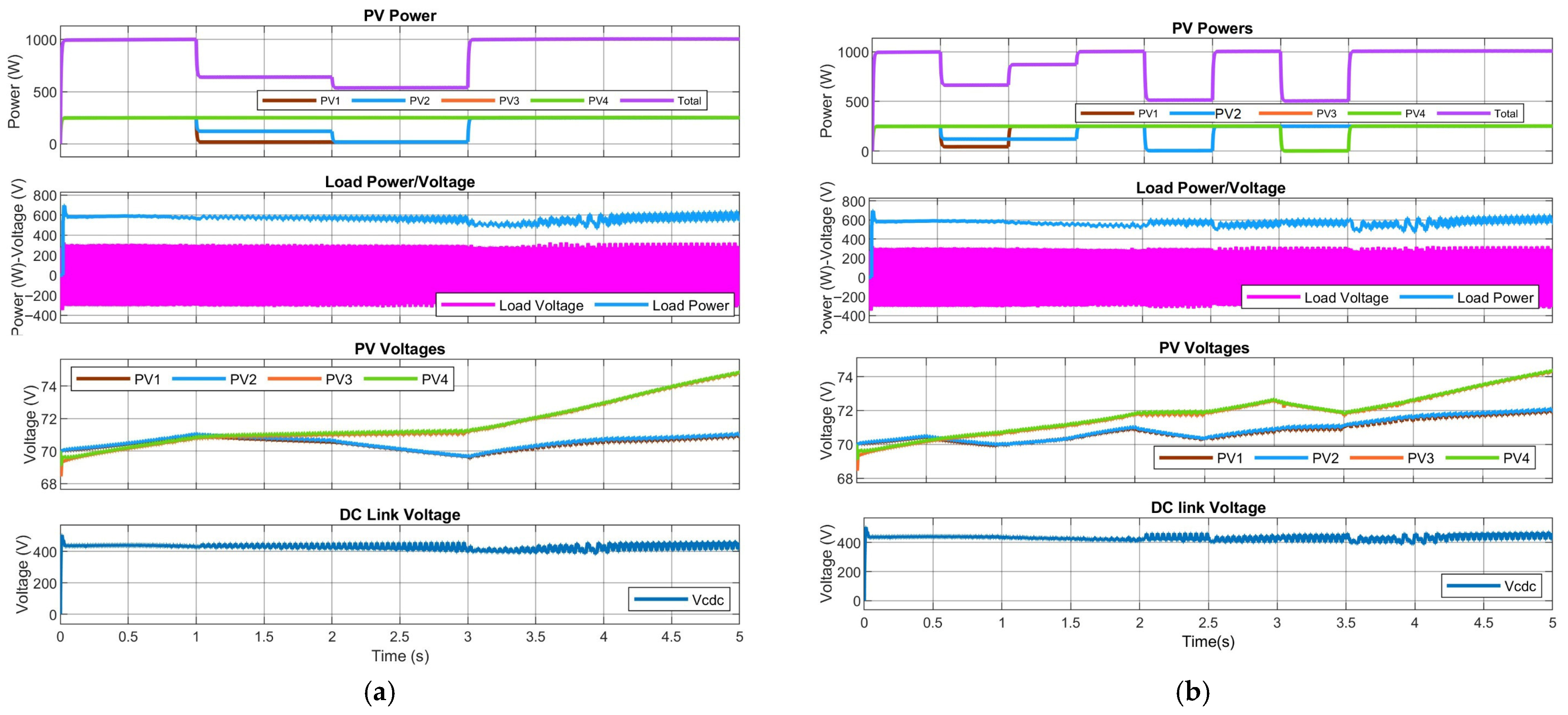
Dynamic variations in irradiance conditions are employed in this scenario, Initially, all PV panels operate at full irradiance. At t = 0.5 s, PV1 is reduced to 20% of irradiance; from 2 to 2.5 s, it is operated at minimum irradiance. In PV2 from 0.5 s, the irradiance is reduced to 50% to 1.5 s and, from 2 to 2.5 s, it is operated at minimum irradiance. In PV3 and PV4, the irradiance is minimum at 3–3.5 s. The outcomes of the dynamic variations in scenario 1 and scenario 2 are presented in Figure 12a and Figure 12b, respectively. PV1 is operated at minimum irradiance from 1 to 3 s, PV2 is operated at 50% irradiance from 1 to 2 s, and it is reduced to minimum from 2 to 3 s, whereas PV3 and PV4 operate at full irradiance.
The PV powers, voltages, and load details are represented in Figure 12. To further assess the system’s dynamic adaptability, two additional irradiance-changing scenarios were simulated. In scenario 1 (Figure 12a), all PV modules operate under 1000 W/m2. At t = 0.5 s, PV1’s irradiance drops to 20% and remains there until 2.5 s, with PV2 experiencing a 50% drop from 0.5 s to 1.5 s, followed by a minimum irradiance level from 2 s to 2.5 s. PV3 and PV4 are subjected to low irradiance from 3 to 3.5 s. The simulation results confirm stable MPPT operation and voltage regulation under these complex transitions. In scenario 2 (Figure 12b), PV1 is maintained at minimum irradiance from 1 s to 3 s, while PV2 is set at 50% irradiance between 1 s and 2 s and then reduced further to minimum irradiance until 3 s. PV3 and PV4, on the other hand, continue operating under full irradiance. These simulation results reinforce the effectiveness of the proposed time-sharing MPPT algorithm, even under sudden and sequential changes in solar irradiance. The control strategy maintains efficient power extraction, ensures regulated voltage, and delivers consistent power to the load, all while using a single MPPT controller across multiple modules.

4. Experimental Results

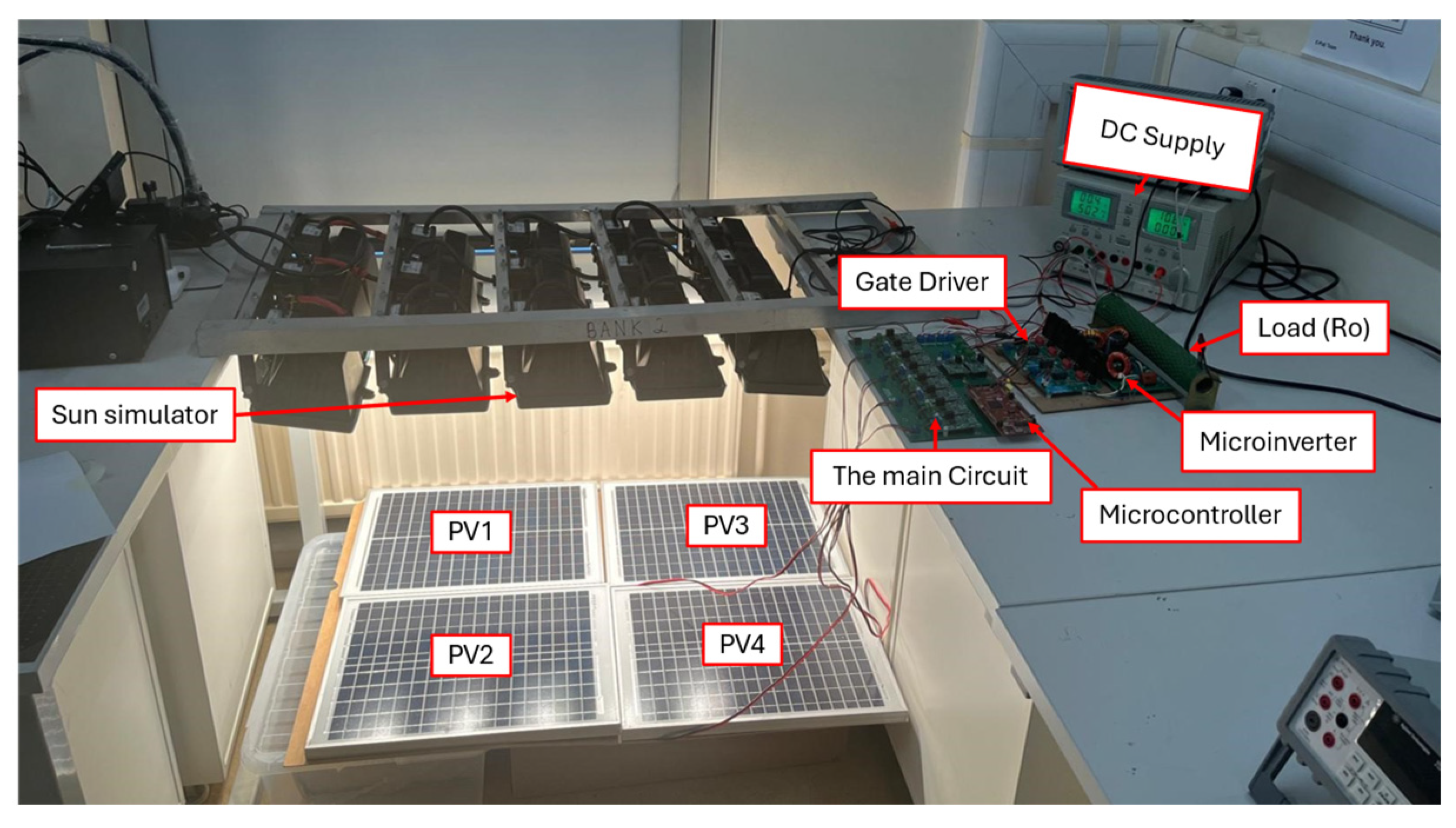
An experimental setup was developed to assess the effectiveness of the proposed control strategy under real-world conditions. The configuration consists of four PV modules, where each pair is connected in parallel and joined at a common midpoint, denoted as N, to enable individual module performance evaluation. The hardware arrangement is depicted in Figure 13. It includes a sun simulator to replicate solar irradiance, a microcontroller DSP TMS320F28379D to implement the control algorithm, and a microinverter circuit integrated with a gate driver and a main power stage. A DC power supply provides system initialization, while a resistive load (Rₒ) is connected at the output to assess operational performance under load conditions. The experimental waveforms are captured by an oscilloscope (Siglent SDS1104X-E). Voltage waveforms are measured by a Micsig differential voltage probe with a 100 MHz bandwidth. The key specifications of the hardware components used in the experiments are listed in Table 4.

4.1. Thermal Analysis

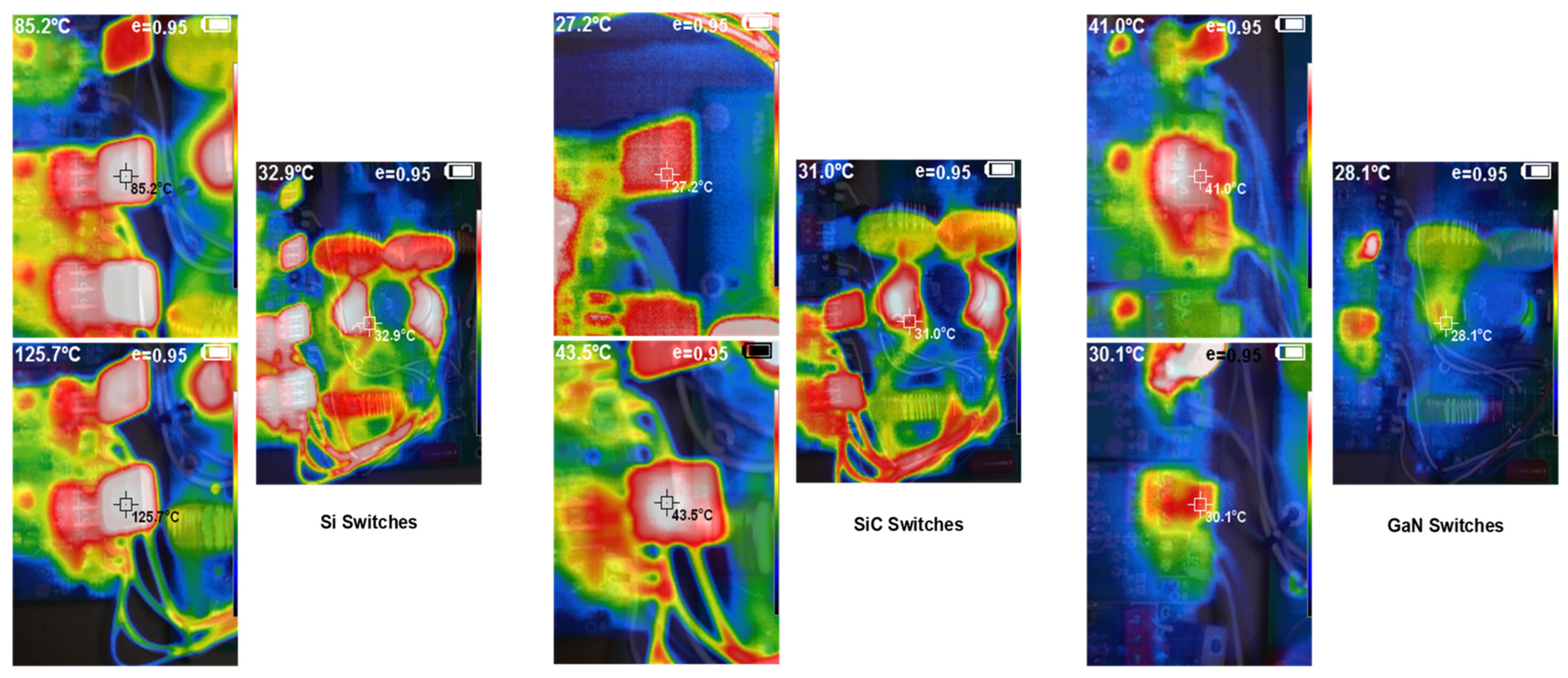
Thermal analysis is a critical aspect of power converter design, as excessive heat can compromise efficiency, reliability, and long-term performance. In high frequency and high-power applications such as the proposed microinverter system, selecting power switches with superior thermal characteristics is essential. To ensure optimal component selection for compact and thermally constrained renewable energy applications, this section presents a comparative evaluation of silicon (Si), silicon carbide (SiC), and gallium nitride (GaN) power switches. The thermal comparison shown in Figure 14 is based on infrared thermal imaging captured using an HT-A1 infrared camera (Hti) through designated temperature monitoring holes. The results reveal the distinct thermal behaviors of each switch technology under identical operating conditions. The Si-based switches exhibit significantly higher surface temperatures, reaching up to 125.7 °C and 85.2 °C, indicating higher conduction and switching losses. These losses translate into increased thermal stress and inefficient heat dissipation.
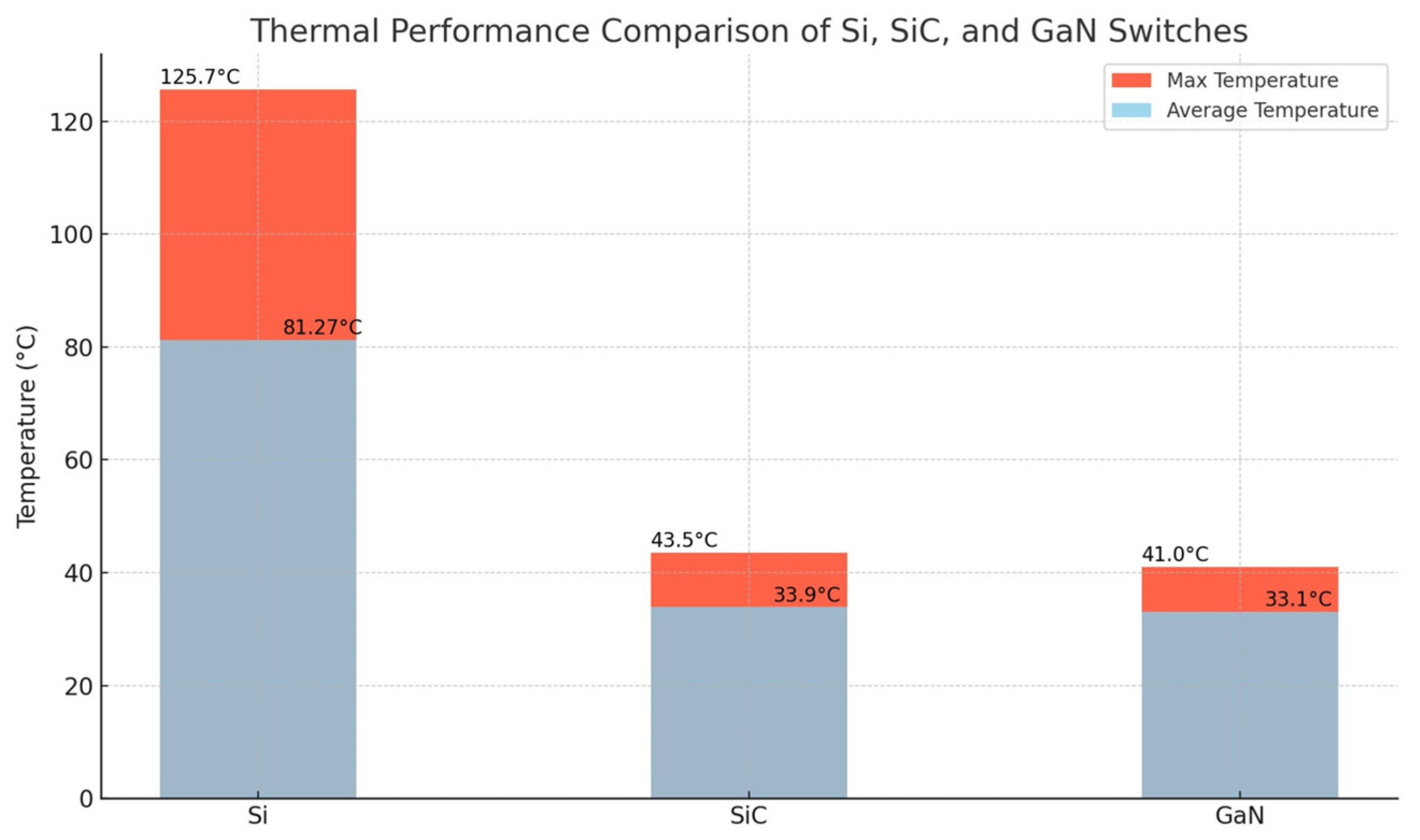
In contrast, SiC switches perform considerably better, with maximum temperatures recorded around 43.5 °C and 31.0 °C. This improved performance is attributed to their superior thermal conductivity and lower switching losses, enabling more uniform heat distribution and better thermal management. GaN switches show the best thermal behavior, with surface temperatures ranging from 28.1 °C to 41.0 °C. Their ultra-fast switching capability and low on-resistance result in minimal and localized thermal footprints, confirming their high efficiency in thermally demanding applications. These findings are further summarized in Figure 15, which presents both the maximum and average temperature values for Si, SiC, and GaN switches. The results highlight the clear thermal advantages of wide bandgap (WBG) devices, with GaN offering the most favorable performance, followed by SiC. Based on this analysis, GaN switches were selected for the experimental prototype due to their excellent thermal efficiency and suitability for compact high-power converter applications in renewable energy systems.
For thermal testing, the GaN devices were operated without external heatsinks to evaluate their intrinsic thermal behavior. The devices were mounted on a PCB with natural convection cooling. All measurements were performed in a laboratory environment at an ambient temperature of 25 °C, without forced airflow. Device conduction and switching losses were estimated from datasheet parameters and experimentally observed switching waveforms. Surface temperature distribution was then recorded using an infrared thermal imaging camera, allowing correlation between the estimated power loss and the measured device temperature. This methodology provides a fair comparison with Si and SiC devices under identical operating conditions.
Figure 16 assesses the performance of the microinverter under the scenario of varying irradiance conditions. Initially, all four PV panels operate at full irradiance. At t = 17 s, PV1 is shaded by 20%, while PV2 is shaded by 50%. Despite this, the microinverter is able to obtain the average maximum power from all panels. At t = 32 s, PV1 returns to full irradiance, but PV2 remains at 50% shading. By t = 50 s, PV2 is also returned to full irradiance. Later, at t = 60 s, PV1 and PV2 are fully shaded, significantly impacting the average maximum power generation, but the microinverter continues extracting power from the unshaded panels. At t = 77 s, PV1 and PV2 return to full irradiance, restoring maximum power generation. At t = 90 s, PV3 and PV4 are fully shaded, reducing power output again, but they return to full irradiance at t = 105 s. The results confirm that the microinverter dynamically adjusts to shading conditions, optimizing power extraction at every stage. These two scenarios collectively demonstrate the robustness and adaptability of the proposed microinverter in handling partial shading and open circuit faults, ensuring efficient power management in a dynamic solar PV environment.
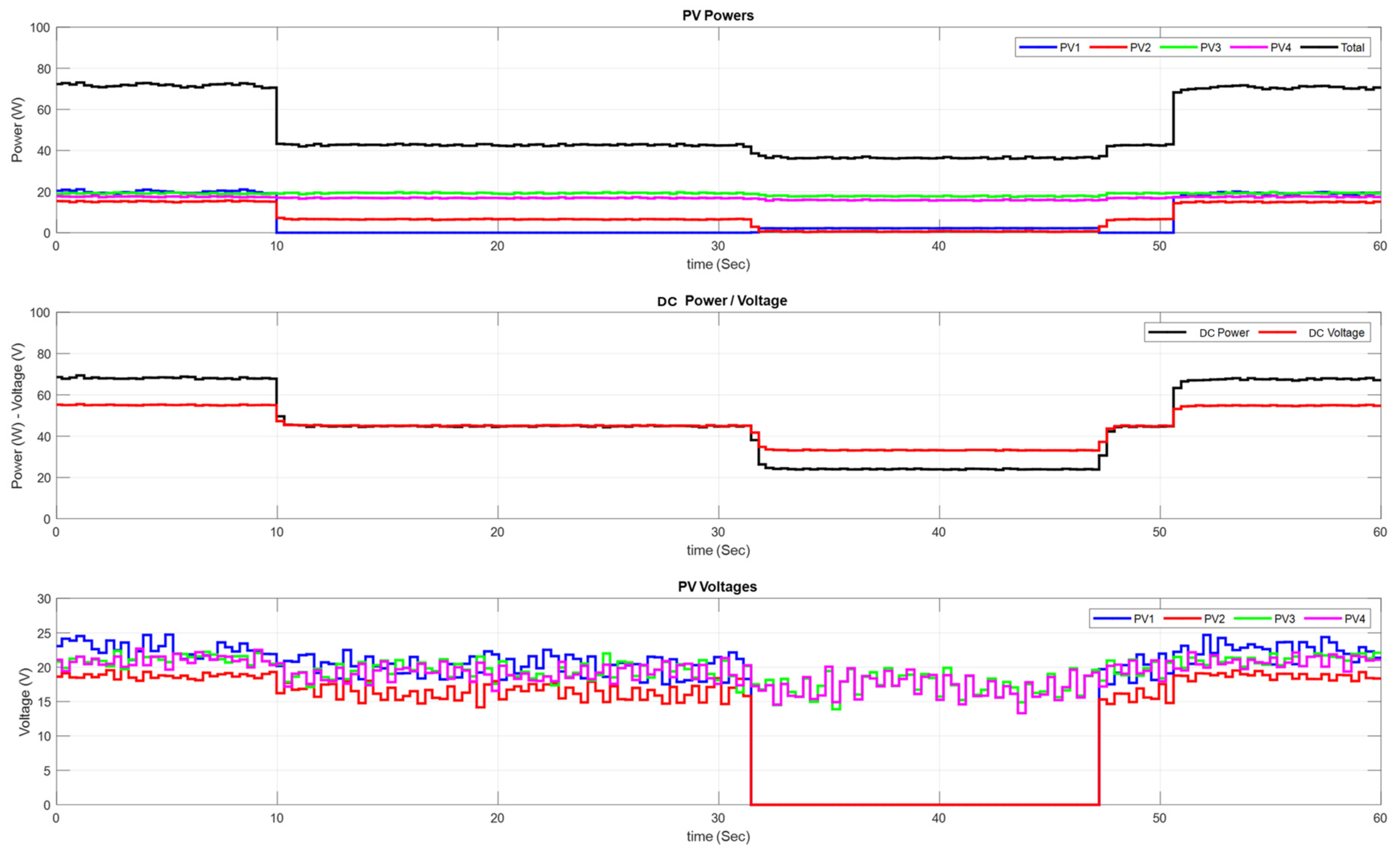
Figure 17 examines the microinverter’s performance scenario when PV panels experience open circuit faults. At t = 10 s, PV1 is disconnected, leading to a 50% power reduction in PV2, while the remaining PV panels continue generating maximum power. At t = 32 s, PV2 also experiences an open circuit fault, further reducing power availability. However, at t = 47 s, PV1 and PV2 are reconnected sequentially, restoring the system to full power operation. The results demonstrate that the inverter can handle open circuit faults efficiently, allowing the system to recover and resume normal operation when faults are cleared.
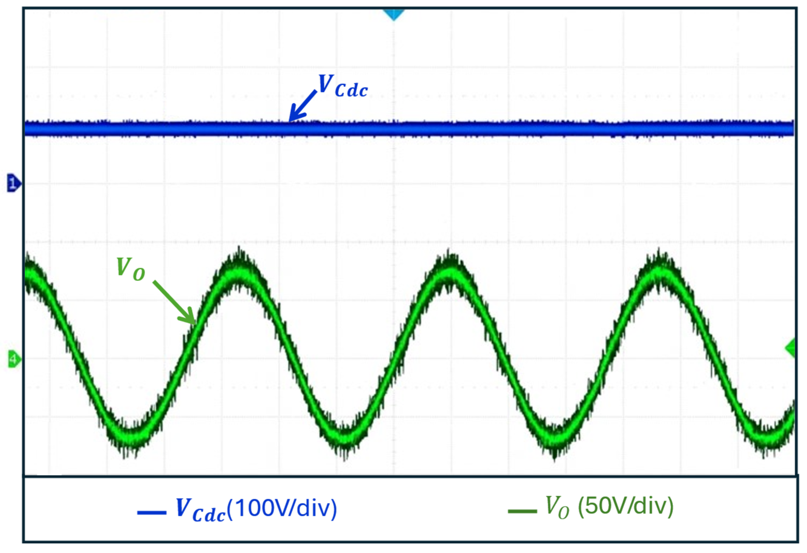
Figure 18 shows the measured waveforms of the inverter operating under maximum power point tracking (MPPT). The DC-link voltage remains nearly constant during operation, demonstrating stable bus regulation under MPPT conditions. The inverter output voltage exhibits a clear sinusoidal waveform with a fundamental frequency of 50 Hz, synthesized using high-frequency pulse-width modulation (PWM) at a switching frequency of 30 kHz. As expected, small high-frequency ripples are superimposed on the sinusoidal waveform due to the switching action of the power devices, although these components are effectively reduced by the output filter. These results confirm that the inverter, when controlled with MPPT, is able to extract maximum power from the PV source while simultaneously delivering a high-quality AC output with minimal distortion. While the current study focuses on maintaining constant output power under varying irradiance, future investigations will consider dynamic load conditions to evaluate system response and efficiency under more variable demand profiles. This will help validate the robustness of the proposed control strategy in broader real-world applications.

4.2. Comparison with Current DMPPT Control Strategies

For a comprehensive assessment of the proposed strategy, two related control strategies—control strategy by [19,22] and [21]—have been selected for comparative analysis. These three control strategies are being thoroughly compared from a range of perspectives. Table 5 summarizes the pros and cons of these strategies. The drawbacks of each strategy are highlighted in bold italics. The proposed algorithm achieves true MPP tracking capability with only a single MPPT unit compared with other algorithms. Furthermore, it enhances the utilization rate of the integrated circuit, thereby reducing overall costs. While [21] proposed a subpanel level time-sharing MPPT using three self-adaptive timings, our approach targeted full module integration with a single controller, improving scalability and reducing control complexity. Furthermore, our strategy was validated under dynamic scenarios, with thermal metrics, which were not addressed in [21]’s experimental scope.
While the experimental validation was limited to four PV modules, the proposed TS-MPPT architecture was designed with scalability in mind, and we have analyzed its feasibility for larger systems. Scaling to configurations with ten or more modules introduces key challenges such as increased switching stress, tighter timing allocation, and greater controller overhead. As the number of modules increases, cumulative switching activity rises, potentially stressing the shared power devices; this issue can be mitigated using wide bandgap semiconductors such as GaN, which offer superior thermal and switching performance. In terms of timing, the control algorithm must allocate sufficient MPPT time slices to each module within a fixed control cycle, and high-speed timers are used to maintain resolution and prevent tracking degradation under fast-changing irradiance. Moreover, as the number of modules grows, the computational burden on the controller increases due to more frequent sensing and MPPT calculations. This can be addressed by using higher-performance digital controllers or parallel processing platforms such as field programmable gate array (FPGA). To further support the scalability claim, simulation results under a 12-module configuration show that the proposed method maintains tracking efficiency above 98% while meeting real-time constraints and thermal limits.

5. Conclusions

Maximizing performance in photovoltaic (PV) systems requires a careful balance between minimizing power losses due to mismatch conditions and managing the complexity introduced by distributed maximum power point tracking (DMPPT) architectures. This study addresses a notable gap in the literature by introducing a novel method for performing MPPT across multiple PV modules using a single-phase non-isolated multi-input microinverter—a configuration not previously explored in the existing research. The proposed architecture integrates a multi-input boost converter into an H-bridge inverter without requiring additional active switching devices, thereby simplifying the circuit structure and enhancing reliability. This integration enables the extraction of multiple system state variables and facilitates more effective and responsive control. Central to this approach is a time-sharing MPPT control strategy that allows a single MPPT unit to sequentially manage multiple PV modules. By updating each module’s MPPT and modulation parameters once per half-cycle of the AC output (approximately every 10 ms), the system achieves high control efficiency, optimized hardware utilization, and significant cost reductions. Comprehensive simulation results under various partial shading conditions confirm that the proposed control method effectively maximizes power extraction and minimizes energy loss. Additionally, experimental validation demonstrates the microinverter’s real-time adaptability and thermal efficiency, particularly using GaN power devices, which offer superior thermal performance compared with conventional Si and SiC counterparts. Overall, the proposed strategy enhances the robustness and scalability of PV systems in dynamic environments, providing a cost-effective and thermally efficient solution for distributed energy systems. Future research will focus on full-scale hardware implementation, scalability analysis for larger PV arrays, and integration with hybrid renewable energy sources to support resilient and adaptive energy management systems.

Author Contributions

Conceptualisation, A.A. and P.C.-K.L.; methodology, A.A. and P.C.-K.L.; software, A.A. and P.C.-K.L.; validation, A.A. and P.C.-K.L.; formal analysis, A.A.; investigation, A.A. and P.C.-K.L.; resources, A.A., P.C.-K.L. and Z.L.; data curation, A.A.; writing—original draft preparation, A.A. and P.C.-K.L.; writing—review and editing, A.A., K.A.I., P.C.-K.L. and Z.L.; supervision, P.C.-K.L. and Z.L All authors have read and agreed to the published version of the manuscript.

Funding

This studentship of the first author was funded by Libyan Cultural Affair/London, Libya with Grant ID 13840.

Data Availability Statement

The data that support the findings of this study are available from the corresponding author upon reasonable request.

Acknowledgments

This research received no external funding.

Conflicts of Interest

The authors declare no conflicts of interest.

Nomenclature

PVPhotovoltaic
PGSPV Generation Systems
FPPFull Power Processing
DPPDifferential Power Processing
MPPTMaximum Power Point Tracking
CMPPTCentralized Maximum Power Point Tracking
DMPPTDistributed Maximum Power Point Tracking
GMPPGlobal Maximum Power Point
GMPPTGlobal Maximum Power Point Tracking
LMPPsLocal Maximum Power Points
TS-MPPTTime-Sharing Maximum Power Point Tracking
CCMContinuous Conduction Mode
DCDirect Current
DCMDiscontinuous Conduction Mode

References

  1. Ruchira; Tamrakar, E.; Patel, R.N.; Choudekar, P. Customized Design of Microinverter Based Solar Photovoltaic System for Small Houses in Developing Nations. Renew. Energy Focus 2022, 42, 178–189. [Google Scholar] [CrossRef]
  2. Mehta, H.K.; Panchal, A.K. A Novel Exponent I–V Relation Based Maximum Power Point Algorithm for Photovoltaic Panel. Renew. Energy Focus 2021, 36, 56–64. [Google Scholar] [CrossRef]
  3. Husain, M.A.; Pingale, S.B.; Bakar Khan, A.; Faiz Minai, A.; Pandey, Y.; Shyam Dwivedi, R. Performance Analysis of the Global Maximum Power Point Tracking Based on Spider Monkey Optimization for PV System. Renew. Energy Focus 2023, 47, 100503. [Google Scholar] [CrossRef]
  4. Satapathy, P.; Dhar, S.; Dash, P.K. An Evolutionary Online Sequential Extreme Learning Machine for Maximum Power Point Tracking and Control in Multi-Photovoltaic Microgrid System. Renew. Energy Focus 2017, 21, 33–53. [Google Scholar] [CrossRef]
  5. Alenezi, A.; Hussain, H.A. A New Control Approach for Least Processed Power Tracking Under Mismatch Conditions in PV Systems Using Differential Power Processing. IEEE Trans. Ind. Appl. 2024, 60, 532–543. [Google Scholar] [CrossRef]
  6. Mäki, A.; Valkealahti, S. Power Losses in Long String and Parallel-Connected Short Strings of Series-Connected Silicon-Based Photovoltaic Modules Due to Partial Shading Conditions. IEEE Trans. Energy Convers. 2012, 27, 173–183. [Google Scholar] [CrossRef]
  7. Sameera; Tariq, M.; Rihan, M.; Ayan, M. A Comprehensive Review on the Application of Recently Introduced Optimization Techniques Obtaining Maximum Power in the Solar PV System. Renew. Energy Focus 2024, 49, 100564. [Google Scholar] [CrossRef]
  8. Kim, K.A.; Krein, P.T. Hot Spotting and Second Breakdown Effects on Reverse I-V Characteristics for Mono-Crystalline Si Photovoltaics. In Proceedings of the 2013 IEEE Energy Conversion Congress and Exposition (ECCE 2013), Denver, CO, USA, 15–19 September 2013. [Google Scholar]
  9. Ko, S.W.; Ju, Y.C.; Hwang, H.M.; So, J.H.; Jung, Y.S.; Song, H.J.; Song, H.-e.; Kim, S.H.; Kang, G.H. Electric and Thermal Characteristics of Photovoltaic Modules under Partial Shading and with a Damaged Bypass Diode. Energy 2017, 128, 232–243. [Google Scholar] [CrossRef]
  10. Guiver, C.; Opmeer, M.R. The Energy-Balance Method for Optimal Control in Renewable Energy Applications. Renew. Energy Focus 2024, 50, 100582. [Google Scholar] [CrossRef]
  11. Ziar, H.; Nouri, M.; Asaei, B.; Farhangi, S. Analysis of Overcurrent Occurrence in Photovoltaic Modules with Overlapped By-Pass Diodes at Partial Shading. IEEE J. Photovolt. 2014, 4, 713–721. [Google Scholar] [CrossRef]
  12. Abudulimu, A.; Wenner, S.L.; Philips, A.B.; Lee, C.; Li, D.B.; Jamarkkatel, M.K.; Zawisza, Z.W.; Neupane, S.; Katakumbura, N.P.; Brau, T.; et al. Bias-Dependent Quantum Efficiency Reveals Recombination Pathways in Thin Film Solar Cells. Adv. Energy Mater. 2025, 15, e01709. [Google Scholar] [CrossRef]
  13. Ncir, N.; El Akchioui, N.; El Fathi, A. Enhancing Photovoltaic System Modeling and Control under Partial and Complex Shading Conditions Using a Robust Hybrid DE-FFNN MPPT Strategy. Renew. Energy Focus 2023, 47, 100504. [Google Scholar] [CrossRef]
  14. Khan, O.; Xiao, W.; Zeineldin, H.H. Gallium-Nitride-Based Submodule Integrated Converters for High-Efficiency Distributed Maximum Power Point Tracking PV Applications. IEEE Trans. Ind. Electron. 2016, 63, 966–975. [Google Scholar] [CrossRef]
  15. Wang, F.; Zhu, T.; Zhuo, F.; Yi, H. An Improved Submodule Differential Power Processing-Based PV System with Flexible Multi-MPPT Control. IEEE J. Emerg. Sel. Top. Power Electron. 2018, 6, 94–102. [Google Scholar] [CrossRef]
  16. Chu, G.; Wen, H.; Jiang, L.; Hu, Y.; Li, X. Bidirectional Flyback Based Isolated-Port Submodule Differential Power Processing Optimizer for Photovoltaic Applications. Sol. Energy 2017, 158, 929–940. [Google Scholar] [CrossRef]
  17. Qin, S.; Barth, C.B.; Pilawa-Podgurski, R.C.N. Enhancing Microinverter Energy Capture with Submodule Differential Power Processing. IEEE Trans. Power Electron. 2016, 31, 3575–3585. [Google Scholar] [CrossRef]
  18. Chu, G.; Wen, H.; Yang, Y.; Wang, Y. Elimination of Photovoltaic Mismatching with Improved Submodule Differential Power Processing. IEEE Trans. Ind. Electron. 2020, 67, 2822–2833. [Google Scholar] [CrossRef]
  19. Khan, O.; Xiao, W. An Efficient Modeling Technique to Simulate and Control Submodule-Integrated PV System for Single-Phase Grid Connection. IEEE Trans. Sustain. Energy 2016, 7, 96–107. [Google Scholar] [CrossRef]
  20. Poshtkouhi, S.; Palaniappan, V.; Fard, M.; Trescases, O. A General Approach for Quantifying the Benefit of Distributed Power Electronics for Fine Grained MPPT in Photovoltaic Applications Using 3-D Modeling. IEEE Trans. Power Electron. 2012, 27, 4656–4666. [Google Scholar] [CrossRef]
  21. Zhu, T.; Wang, F.; Fan, Y.; Zhuo, F. Subpanel Level Time-Sharing Maximum Power Point Tracking System with Self-Adaptively Adjusted Control Strategy. In Proceedings of the 2015 IEEE 2nd International Future Energy Electronics Conference (IFEEC 2015), Taipei, Taiwan, 1–4 November 2015. [Google Scholar]
  22. Cao, Z.; Li, Q.; Lee, F.C. Multi-Phase Smart Converter for PV System. In Proceedings of the Conference Proceedings—IEEE Applied Power Electronics Conference and Exposition (APEC 2015), Charlotte, NC, USA, 15–19 March 2015; Volume 2015. [Google Scholar]
  23. Madeti, S.R.K. A Monitoring System for Online Fault Detection in Multiple Photovoltaic Arrays. Renew. Energy Focus 2022, 41, 160–178. [Google Scholar] [CrossRef]
  24. Mazumdar, D.; Biswas, P.K.; Sain, C.; Ahmad, F.; Ustun, T.S.; Kalam, A. Performance Analysis of Drone Sqadron Optimisation Based MPPT Controller for Grid Implemented PV Battery System under Partially Shaded Conditions. Renew. Energy Focus 2024, 49, 100577. [Google Scholar] [CrossRef]
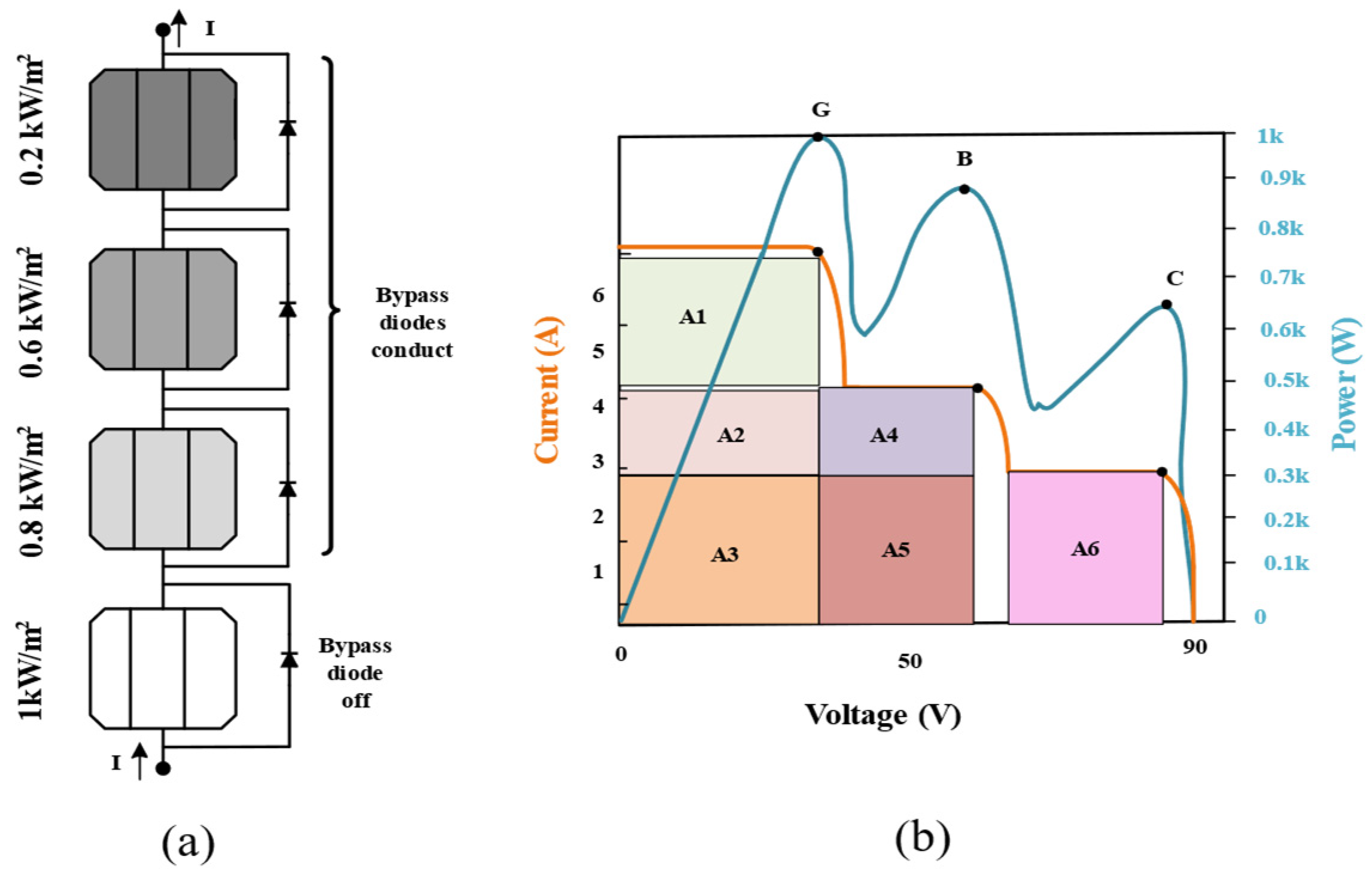
Figure 1. Effects of partial shading in the PV system. (a) Current flow in the PV string with two partial-shaded modules. (b) Output I–V curve and P–V curve.
Energies 18 04925 g001
Figure 2. Proposed non-isolated multiple-input MI.
Energies 18 04925 g002
Figure 3. Current flow paths associated with the four switching modes of the proposed MI: (a) null-1 (00), (b) active-1 (01), (c) active-2 (10), and (d) null-2 (11).
Energies 18 04925 g003
Figure 4. Control system algorithm: (a) time-sharing MPPT control and (b) the framework of clock signal.
Energies 18 04925 g004
Figure 5. Control system block diagram.
Energies 18 04925 g005
Figure 6. Control system time-sharing signal.
Energies 18 04925 g006
Figure 7. Simulated I–V and P–V characteristics of PV.
Energies 18 04925 g007
Figure 8. Performance of PV modules during fixed irradiance condition: (a) PV current, (b) PV power, and (c) PV voltage.
Energies 18 04925 g008
Figure 9. Voltage of PV modules during varying irradiance.
Energies 18 04925 g009
Figure 10. Modules during varying irradiance: (a) PV current and (b) PV power.
Energies 18 04925 g010
Figure 11. Varying irradiation condition output load: (a) power, (b) DC-link voltage, and (c) output current and voltage.
Energies 18 04925 g011
Figure 12. Dynamic simulation results: (a) scenario 1 and (b) scenario 2.
Energies 18 04925 g012
Figure 13. Experimental setup.
Energies 18 04925 g013
Figure 14. Thermal imaging comparison of Si, SiC, and GaN switches under operation.
Energies 18 04925 g014
Figure 15. Maximum thermal performance comparison of Si, SiC, and GaN switches.
Energies 18 04925 g015
Figure 16. Experimental results during first scenario.
Energies 18 04925 g016
Figure 17. Experimental results during second scenario.
Energies 18 04925 g017
Figure 18. Microinverter output voltage and DC-link voltage under MPPT operation.
Energies 18 04925 g018
Table 1. Comparison between two DMPPT structures.
Characteristic ComparisonDPPFPP
PV cell group couplingHighLow
DC-DC converter couplingHighLow
Priority of bidirectional converterHighLow
Cable demandHighLow
CommunicationYesNo
Ease of system expansionModerateFlexible
Number of convertersn × mn
Control designMultipleMPPT
MPPT granularity (no modification of PV panel)HighLow
Table 2. Charging and discharging state of all the components.
StatesPositive FHC (Vo > 0)Negative FHC (Vo < 0)
Null-1 (00)Active-1 (10)Null-2 (11)Null-1 (00)Active-2 (01)Null-2 (11)
L1Non-activeNon-activeActiveNon-activeActiveActive
L2ActiveActiveNon-activeActiveNon-activeNon-active
Cdc (Ic)Active
(IL1+)
Non-active
(iO − iL1+)
Active
(IL2+)
Active
(IL1)
Non-active
(iO − iL1+)
Active
(IL2)
DurationMdc1, Ts(d1 − Mdc1) Ts(1 − d1) Tsd1 Ts(Mdc2 − d1) Ts(1 − Mdc2) Ts
Table 3. Simulation specifications.
ParameterSpecification
4 input PV panels (Vmpp)70 v
Output AC (Vo)220 Vrms,
Modulation indexesMac = 0.8; Mdc1 = 0.17
Carrier frequency (kHz)30
Inductors L1, L2 (µH)450
DC-link capacitor Cdc (µF)440
Table 4. Hardware component specifications.
ParameterSpecification
Open circuit voltage (Voc)23 V
Short circuit current (Isc)2 A
Carrier frequency (kHz)30
Inductors L1, L2 (µH)450
DC-link capacitor Cdc (µF)440
Diodes D1, D2FFSH1665A
Power switches S1-S4TP65H150G4PS (650 V, Ron = 180 mΩ)
Table 5. Comparison of proposed strategy with existing DMPPT control strategies.
Control Strategy.[19][22][21]Proposed
Real MPP trackingyesnopartiallyyes
Number of MPPT units3131
Utilization of MPPT unitlowhighmediumhigh
Existence of OPRyesnoyesyes
Costhighlowmediumlow
Disclaimer/Publisher’s Note: The statements, opinions and data contained in all publications are solely those of the individual author(s) and contributor(s) and not of MDPI and/or the editor(s). MDPI and/or the editor(s) disclaim responsibility for any injury to people or property resulting from any ideas, methods, instructions or products referred to in the content.