Article

Power Factor Adaptive DPWM Control Strategy for T-Type Three-Level Inverters

by
Jialiang Tian
,
Yingying Xu
,
Mingxia Xu
*,
Zhenjiang Liu
and
Yuchi Zhou
School of Electrical Engineering, Dalian Jiaotong University, Dalian 116052, China
*
Author to whom correspondence should be addressed.
Energies 2025, 18(17), 4574; https://doi.org/10.3390/en18174574
Submission received: 25 July 2025 / Revised: 18 August 2025 / Accepted: 21 August 2025 / Published: 28 August 2025
(This article belongs to the Special Issue Advanced Power Electronics Technology: 2nd Edition)

Abstract

With the widespread application of multilevel inverters, device losses have become a critical area of research. A key limitation of conventional three-level discontinuous pulse width modulation (DPWM) strategies is their inability to maintain switching device clamping during the peak intervals of the load current, especially under varying load power factor conditions, thereby reducing switching losses. This paper proposes an improved three-level power factor adaptive DPWM (PFA-DPWM) strategy that minimizes switching losses by clamping the power devices during the one-third fundamental period of maximum load current. First, a unified mathematical model of DPWM strategies is established. Theoretical analysis demonstrates that phase disposition (PD) carrier modulation for three-level inverter exhibits superior line voltage harmonic characteristics. Based on this, a theoretical comparison of switching losses and harmonic distortion for various DPWM schemes is conducted. The proposed PFA-DPWM control strategy has the minimum switching loss without compromising harmonic performance. The efficacy and validity of the proposed strategy are confirmed by comprehensive simulation and experimental results.

1. Introduction

The accelerated proliferation of renewable energy, particularly wind and solar photovoltaics, has resulted in a substantial increase in their global installed capacity. Consequently, multilevel converters have become a prominent research topic owing to their advantages, particularly low harmonic distortion in the output voltage and reduced voltage stress on switching devices [1,2,3]. However, the issue of losses in power electronic switching devices has become increasingly significant, constraining the trend toward modular and lightweight designs for power electronic systems. Therefore, optimizing PWM control strategies to improve system efficiency, without altering the hardware circuit, has emerged as a key approach for the efficiency optimization of power electronic devices.
The PWM control strategies for multilevel inverters primarily include sinusoidal pulse-width modulation (SPWM) [4], space vector pulse-width modulation (SVPWM) [5,6], and discontinuous pulse-width modulation (DPWM). Among these, the three-level DPWM strategy can keep the switching devices inactive for one-third of a fundamental period, thereby reducing switching losses. This strategy can effectively improve system efficiency.
The research in refs. [7,8,9] investigates the zero-sequence component injection methods for various two-level DPWM strategies, derives the intrinsic relationship between two-level continuous and discontinuous PWM, and establishes a unified modulation function including SPWM, SVPWM, and various DPWM schemes. In the three-level inverter circuit, the neutral-point potential is regulated using medium and small vectors. However, conventional DPWM strategies exhibit challenges in maintaining neutral-point balance, particularly at a high modulation index. To address this issue, a DPWM strategy based on carrier common mode voltage suppression is proposed to solve the influence of clamping mode on neutral-point current [10]. A novel suppressed common-mode voltage DPWM (SCMV-DPWM) strategy is proposed, which achieves neutral-point (NP) voltage balance by the active regulation of the injected zero-sequence voltage. The control strategy is derived from a NP current model that links the zero-sequence voltage to the resulting NP current, thereby enabling precise voltage regulation in each switching cycle [11]. In the case of increasing the clamping state “0”, the clamping state with the minimum output current ripple is selected for optimal distribution by averaging the current vector amplitude, thereby enhancing the quality of the output current [12]. Traditional DPWM strategies are characterized by a fixed clamping interval, which leads to low-order harmonics in the output current and suboptimal neutral-point voltage balancing performance. A carrier-based DPWM (CB-DPWM) method that employs a variable clamping interval is proposed to concurrently suppress low-order harmonics and enhance the NP voltage balancing capability [13]. In ref. [14], taking the three-phase Vienna rectifier as an example, the common-mode voltage characteristics of different DPWM types are analyzed, and a reverse carrier modulation method to suppress the common-mode voltage is proposed. A dynamic space vector DPWM (DSV-DPWM) method is proposed in ref. [15] to solve the problem of AC input current distortion caused by the unbalanced neutral voltage of the three-level converter. By optimizing the modulation strategy, the vector deviation is eliminated, and the current harmonics are effectively reduced. A method is proposed in ref. [16] to select the operating region based on the phase angle of the reference signal and superimpose the common-mode signal on the reference signal to reduce both the output voltage THD and switching losses. A hybrid DPWM scheme was proposed to achieve neutral-point voltage self-balancing and enhanced power density through a synergistic combination of variable switching frequency and modulation mode selection [17,18]. Modulation methodologies for Cascaded H-Bridge Multilevel Inverters are implemented to enhance power conversion efficiency and harmonic performance in output voltages [19,20]. Furthermore, an optimized DPWM method was proposed in ref. [21], providing deeper insight into the relationship between common-mode voltage and leakage current. The common-mode voltage characteristics of space vectors under different NP conditions are analyzed, and the switching state sequence is optimized to minimize the common-mode voltage to mitigate leakage current. An improved DPWM strategy is proposed to concurrently balance NP voltage, suppress common-mode resonant current, and reduce switching losses. The strategy partitions the 60° DPWM1 clamping interval into three sub-intervals, shortening the net clamping duration to mitigate NP voltage deviations and simplify control. Predefined NP voltage limits the control trade-off between maintaining NP voltage balance and suppressing common-mode current. An offset voltage is then injected to modulate the clamping states, ultimately satisfying all control objectives [22]. The research in refs. [23,24,25,26] comprehensively analyzes the voltage harmonic characteristics and switching losses of various PWM strategies for three-phase inverters under different modulation indices, summarizing the respective advantages, disadvantages, and suitable application scenarios for the strategies.
Conventional DPWM control strategies primarily rely on zero-sequence component injection to transition among different modulation strategies. However, the injected zero-sequence component is derived from the modulation voltage signal, without considering the impact of load current phase on system performance. Specifically, the switching losses of DPWM control strategies exhibit a positive correlation with the instantaneous load current. Consequently, to achieve minimum switching losses, it is imperative that the device clamping interval during the one-third of the fundamental period coincides with the peak absolute load current.
Conventional three-level DPWM strategies fail to track real-time variations in the load power factor (i.e., the current phase angle). This paper proposes a novel three-level power factor adaptive DPWM (PFA-DPWM) strategy to minimize switching losses. The proposed strategy is developed based on an analysis of the unified explicit modulation function for three-level PWM and a load power factor detection model. Furthermore, a harmonic analysis of different three-level carrier-based modulation schemes, particularly phase disposition (PD), phase opposition disposition (POD), and alternative phase opposition disposition (APOD), is conducted. The results indicate that the PD carrier modulation yields superior voltage harmonic characteristics. Finally, a theoretical analysis compares the harmonic performance of the PFA-DPWM strategy with modulation strategies. The simulation and experimental results proposed to verify the practical efficacy of the proposed PFA-DPWM strategy.

2. Three-Level PFA-DPWM Strategy

Taking the T-type three-level inverter as a representative topology, this study derives the intrinsic relationship between various three-level DPWM strategies and the zero-sequence component. Subsequently, the mathematical model of the PFA-DPWM strategy is established.

2.1. Basic Principle of Three-Level DPWM

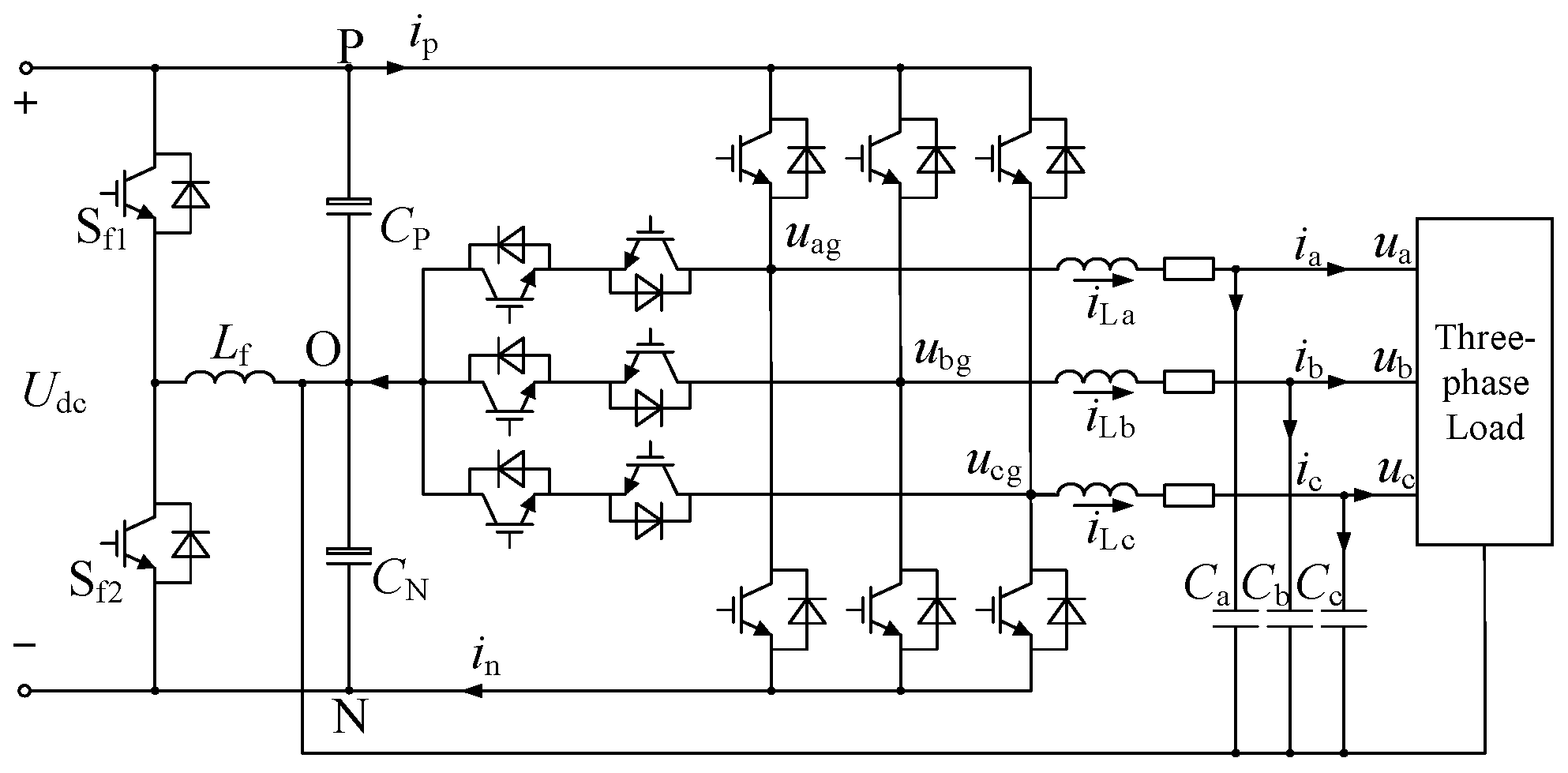
Compared to the NPC inverter, the power loss of the T-type inverter is lower [27]; therefore, this study utilizes a T-type three-level inverter topology, illustrated in Figure 1, which is augmented with a fourth bridge leg (Sf1, Sf2) to achieve precise neutral-point voltage control and enhance load imbalance performance. The operational principle of the inverter is analyzed by examining a phase x (where x ∈ {a, b, c}), and the midpoint of the DC-link capacitors, denoted as “O”, serves as the zero-voltage reference potential. A fundamental operating constraint of the T-type topology dictates that the upper and lower bridge switches, Sx1 and Sx4, cannot conduct simultaneously. Furthermore, the switching states of the device pairs Sx1, Sx3 and Sx2, Sx4 are complementary. Consequently, three distinct voltage values udc/2, 0, and −udc/2 are available at the output of the T-type three-level converter, which correspond to three states (“P”, “O”, and “N”).
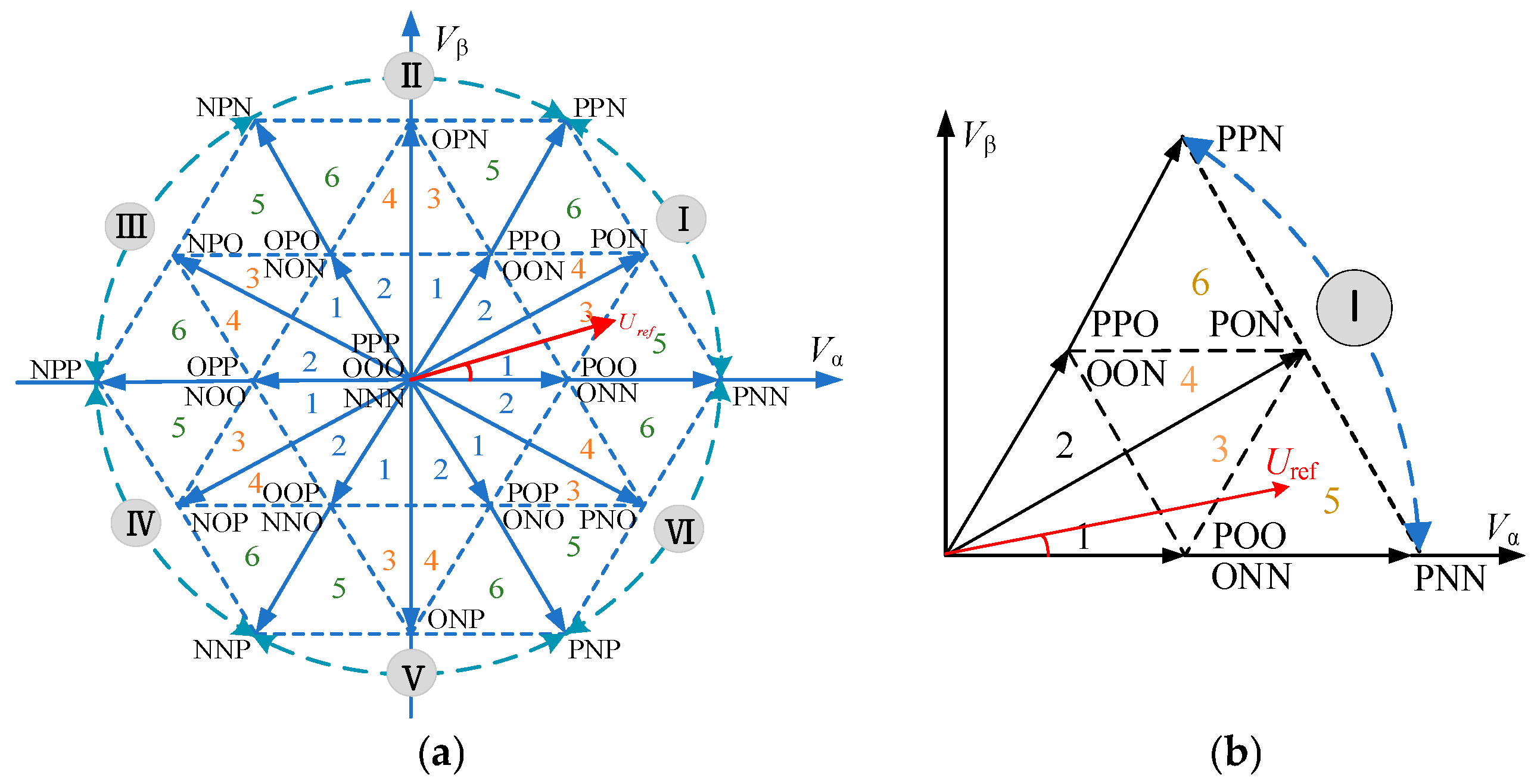
The fundamental space vector diagram for a three-level inverter is presented in Figure 2a. The diagram is partitioned into six primary sectors and comprises 27 distinct voltage vectors, each of which represents an available switching state. Conventional three-level space vector modulation synthesizes the reference voltage vector by applying a combination of the three nearest adjacent vectors. Of particular note are the small voltage vectors, each of which has two redundant switching states: a P-type and an N-type.
To reduce switching losses, the DPWM strategy operates by clamping a phase leg to either the positive or negative DC bus during a specific interval of the fundamental period. This action effectively reduces the number of switching transitions per fundamental period, thereby transforming the conventional seven-segment switching pattern of SVPWM into a five-segment one. In this process, the selection of the appropriate redundant small vector is determined by the clamped-phase state. For instance, to synthesize a reference vector located in sub-sector 5 of Sector I, phase-a is clamped to P-level, and the reference is synthesized using the three nearest voltage vectors. This principle is extended to remaining sectors, with the resulting complete vector distribution illustrated in Figure 2b.

2.2. Mathematical Model of Traditional Three-Level DPWM Strategy

Conventional DPWM strategies include DPWM0, DPWM1, DPWM2, DPWM-Max, and DPWM-Min, etc. This paper establishes a unified mathematical model for a variety of three-level PWM schemes by zero-sequence component injection. This approach avoids the complex coordinate transformations, sector identification, and vector dwell-time calculations inherent to SVPWM, thereby facilitating straightforward digital implementation.
The three-phase output voltage is expressed as
u a = U m sin ω t u b = U m sin ω t 2 π / 3 u c = U m sin ω t 4 π / 3
where Um = 2M*udc/3, M is the modulation index, and udc is the DC bus voltage.
According to the intrinsic relationships among three-level PWM control schemes, a unified mathematical model encompassing various continuous and discontinuous strategies can be formulated through the appropriate injection of a zero-sequence component. This model is expressed as
u ma * = u a + u z u mb * = u b + u z u mc * = u c + u z
u z = ( 2 k 1 ) k u max ( 1 k ) u min u max = max u a , u b , u c u min = min u a , u b , u c
where u ma * , u mb * and u mc * denote the modulation signals of three-phase voltages, uz is the zero-sequence component, k ∈ [0, 1] is the splitting ratio for the different types of zero vectors, and umax and umin are the maximum and minimum values of three-phase voltage.
In the abc coordinate system, the three-phase sinusoidal modulating signals (ua, ub, and uc), are combined with an injected zero-sequence component uz. By varying the parameter k, the allocation of action time for the zero vectors is adjusted, which in turn determines the specific modulation strategy for each modulation period. When k = 1, the DPWM-Max control mode is realized, and only the zero vector (PPP) is used. When k = 0, the DPWM-Min control mode is realized, and only the zero vector (NNN) is used. Furthermore, by alternating the value of k between 0 and 1 at every 60° sector boundary, the DPWM0~2 control mode can be realized. Consequently, the mathematical expression for the zero-sequence component in conventional DPWM strategies can be unified as follows:
u z = 1 u max , II , IV , VI Sector 1 u min , I , III , V Sector DPWM 0 1 u max , if u max > u min 1 u min , if u max < u min DPWM 1 1 u max , I , III , V Sector 1 u min , II , IV , VI Sector DPWM 2 1 u max DPWM-Max 1 u min DPWM-Min

2.3. Mathematical Model of Three-Level PFA-DPWM Strategy

A method for detecting the instantaneous load power factor was previously presented by the authors in ref. [28] and will not be reiterated here. DPWM strategies mitigate switching losses by alternately remaining the power devices inactive for one-third of the fundamental period, an interval during which no switching occurs.
By utilizing the modulating voltage, phase-shifted by the power factor angle, as the condition for configuring the zero-sequence component, a mathematical model for the proposed PFA-DPWM strategy can be derived as follows
u a ( φ ) = u a ( ω t φ ) u b ( φ ) = u b ( ω t φ ) u c ( φ ) = u c ( ω t φ )
where u a , u b , and u c denote the original phase voltages. u a ( φ ) , u b ( φ ) and u c ( φ ) denote the phase voltages after being phase-shifted by the load power factor angle φ.
The maximum and minimum values of the original and phase-shifted voltages are shown as follows:
u max = max u a , u b , u c u min = min u a , u b , u c u max ( φ ) = max u a ( φ ) , u b ( φ ) , u c ( φ ) u min ( φ ) = min u a ( φ ) , u b ( φ ) , u c ( φ )
Therefore, the zero-sequence voltage function of three-level PFA-DPWM can be expressed as
u mz ( φ ) = 1 u min , i f u max ( φ ) < u min ( φ ) 1 u max , i f u max ( φ ) > u min ( φ )
u ma * ( φ ) = u a + u mz ( φ ) u mb * ( φ ) = u b + u mz ( φ ) u mc * ( φ ) = u c + u mz ( φ )
where u mz ( φ ) is the zero-sequence voltage of the three-level PFA-DPWM. u ma * ( φ ) , u ma * ( φ ) , and u mc * ( φ ) are the modulation voltages of the three-level PFA-DPWM.
Figure 3 shows the modulation waveforms for various PWM control strategies at a power factor angle of φ = π/12. The PFA-PWM strategy can maintain clamping of the power device during one-third of the fundamental period at maximum load current.

3. Analysis of Different Three-Level Carrier Modulation Schemes

Beyond the fundamental component, the output voltage also contains harmonic components generated during the switching process. Therefore, characterizing the distribution and magnitude of these harmonics is crucial for the selection of a carrier modulation strategy and the design of output filters. This section quantitatively analyzes the harmonic component of the output voltage by applying the double Fourier series method [29].
The carrier modulation schemes can be categorized as either sawtooth or triangular. Given that triangular carriers offer superior harmonic characteristics, the subsequent analysis is confined to modulation schemes that employ them. There are three common triangular carrier-based modulation schemes:
(1)
PD: All carrier signals are mutually in phase.
(2)
POD: The carriers above the zero reference are phase-shifted by 180° relative to those below it.
(3)
APOD: Each carrier is phase-shifted by 180° with respect to its adjacent carriers.
For three-level inverters, the POD and APOD schemes are functionally equivalent. Consequently, they are consolidated into a single analytical category, as illustrated in Figure 4.
To facilitate the analysis, the carrier functions fc+(x), fc−(x), and the modulating function fm(y), are defined as shown in Table 1. The phase voltage switching function for the PD modulation scheme fPD(x, y) is presented in Table 2. Similarly, the function for the POD/APOD schemes fPOD/APOD(x, y) is given in Table 3, where x = ωct, y = ωmt + θm [30,31].
The voltage switching function fPOD/APOD(x, y) is a bivariate function. Consequently, it is expressed by a double Fourier series expansion as follows [30]
f ( x , y ) = A 00 2 + n = 1 { A 0 n cos [ n ( ω 0 t + θ 0 ) ] + B 0 n sin [ n ( ω 0 t + θ 0 ) ] } + m = 1 { A m 0 cos [ m ( ω c t + θ c ) ] + B m 0 sin [ m ( ω c t + θ c ) ] } + m = 1 n = ± 1 ± A m n cos [ m ( ω c t + θ c ) + n ( ω 0 t + θ 0 ) + B m n sin [ m ( ω c t + θ c ) + n ( ω 0 t + θ 0 )
where
A m n = 1 2 π 2 - π π - π π f ( x , y ) cos ( m x + n y ) d x d y
B m n = 1 2 π 2 - π π - π π f ( x , y ) sin ( m x + n y ) d x d y
By applying the double Fourier series method from (9), the expression for the phase voltage harmonic analysis in the PD modulation can be obtained:
f PD ( x , y ) = V dc M cos ( ω o t + θ o ) 2 + 4 V dc π 2 m = 1 1 2 m 1 k = 1 J 2 k - 1 [ ( 2 m 1 ) π M ] 2 k 1 cos [ ( 2 m 1 ) ω c t ] + V dc π 2 m = 1 1 2 m n = - J 2 n + 1 ( 2 m π M ) cos n π cos [ 2 m ω c t + ( 2 n + 1 ) ( ω o t + θ o ) ] + 4 V dc π 2 m = 1 1 2 m 1 n = - ( n 0 ) k = 1 J 2 k - 1 [ ( 2 m 1 ) π M ] ( 2 k 1 ) ( 2 k 1 + 2 n ) ( 2 k 1 2 n ) cos n π × cos [ ( 2 m 1 ) ω c t + 2 n ( ω o t + θ o ) ]
Similarly, the expression for the phase voltage harmonic components in the POD/APOD modulation can be obtained:
f POD / APOD ( x , y ) = V dc M cos ( ω o t + θ o ) 2 + V dc π 2 m = 1 1 m n = ( n 0 ) J 2 n + 1 ( m π M ) cos n π cos [ m ω c t + ( 2 n + 1 ) ( ω o t + θ o ) ]
Based on (10) and (11), the harmonic component expression of the line-to-line voltage fab(x, y) can be expressed as
f ab ( x , y ) = f a ( x , y ) f b ( x , y )
For a modulation index of M = 0.8 and a carrier ratio of fc/fm = 50, the spectra for the phase-a voltage under the PD and POD/APOD modulation schemes are illustrated in Figure 5. The corresponding line-to-line voltage (ab voltage) spectra are illustrated in Figure 6.
As derived by (10) and visually corroborated by the spectral analyses in Figure 5 and Figure 6, the harmonic components of the PD modulation scheme exhibit the following characteristics:
(1)
The phase voltage contains abundant harmonic components at the carrier frequency. These carrier harmonics are common-mode components and are inherently canceled in the line-to-line voltage.
(2)
Harmonics with even-order sidebands are present around odd multiples of the carrier frequency, and harmonics with odd-order sidebands are present around even multiples of the carrier frequency.
Following a similar procedure, the harmonic characteristics for the POD/APOD modulation schemes can be formulated based on (11), as illustrated in Figure 5 and Figure 6:
(1)
The phase voltage spectrum does not contain odd-order carrier frequency harmonics; only their sideband harmonic components are present. Consequently, the harmonic energy is dispersed among them.
(2)
The odd-order sideband harmonics surrounding even multiples of the carrier frequency are identical to those produced by the PD scheme.
Although the phase voltage THD is nearly identical for both PD and POD/APOD schemes, the line-to-line voltage THD for the PD scheme is significantly lower. This performance difference arises because, in the line-to-line voltage of the POD/APOD schemes, harmonic cancelation is less effective; specifically, only the triplen sideband harmonics around carrier are canceled. As a result, a greater amount of harmonic energy is retained.
Therefore, based on its superior line-to-line voltage harmonic profile, the PD modulation scheme is selected for implementation in this study.

4. Performance Analysis of Three-Level DPWM Strategies

Harmonic distortion and switching loss are critical factors in the selection of a DPWM strategy. This section will, therefore, present a theoretical derivation of these performance metrics for various DPWM strategies to establish the evaluation criteria for an optimal selection.

4.1. Harmonic Distortion

Harmonic distortion is an important parameter for evaluating different PWM control strategies. Assuming the average internal electromotive force (EMF) of the load exy, is constant within any given switching period and neglecting load losses, multiple switching states exist for a specific load EMF condition. For instance, when exy > 0, there are four possible switching combinations within a single carrier period, as shown in Figure 7.
For the case where 0 > ux > uy, the current ripple through the load during the time intervals T1, T2, and T3 can be defined as
Δ i x y ( t ) = e x y L σ t 0 t T 1 Δ i x y ( t ) = V dc e x y L σ ( t T 1 ) e x y L σ T 1 T 1 < t T 1 + T 2 Δ i x y ( t ) = e x y L σ ( t T 1 T 2 ) + V dc e x y L σ T 2 e x y L σ T 1 T 1 + T 2 < t T 1 + T 2 + T 3
where Lσ is the line-to-line equivalent leakage inductance and exy is the average internal electromotive force of the load, x, y ∈ {a, b, c}.
By substituting t = T1 + T2 + T3 = ΔT/2 into (13), the following expression is obtained:
Δ i x y ( Δ T 2 ) = e x y L σ T 3 + V dc e x y L σ T 2 e x y L σ T 1 = 0
From Equation (14), the following can be derived
T 2 = ( u x u y ) Δ T / 2
where u x = e x V dc , u y = e y V dc , then u x u y = e x y V dc .
Similarly, the expressions of T1 and T3 can be obtained:
T 1 = ( 1 + u y ) Δ T / 2 T 3 = ( u x ) Δ T / 2
The mean square value of the current ripple in ΔT/2 is given by (17)
Δ i xy 2 = V dc L σ 2 2 Δ T 0 T 1 ( u y u x ) 2 t 2 d t + 0 T 2 [ ( 1 + u y u x ) x + ( u y u x ) T 1 ] 2 d x + 0 T 3 [ ( u y u x ) x + ( 1 + u y u x ) T 2 + ( u y u x ) T 1 ] 2 d x
where x = tT1, x= tT1T2.
By substituting T1, T2, and T3 into (17), the following expression is obtained:
Δ i xy 2 = V dc L σ 2 Δ T 2 12 ( u x u y ) 2 [ u x 2 + u x ( 1 + u y ) + ( 1 + u y ) 2 ]
Following a similar procedure, the time intervals T1, T2, T3, and the corresponding current ripple for the three switching combinations depicted in Figure 7b–d is derived, with the results summarized in Table 4.
From the above derivations, the harmonic distortion for each modulation strategy can be obtained. For example, the SPWM harmonic distortion is given by (19), and the detailed derivation of (19) is provided in the Appendix A.
F SPWM M = 4 π 3 3 4 M 2 3 + 4 3 2 M 3 + 9 π 8 M 4 0 < M 3 3 ( 2 + 9 M 2 ) arccos ( 1 3 M ) + 3 3 + 4 π 4 M 2 3 + 4 3 2 M 3 ( 11 3 + 4 M 2 ) 3 M 2 1 + 9 π 8 M 4 M > 3 3
The mean square value of the total harmonic current for SVPWM is given by
  F SVPWM M = 1 768 720 + 256 3 M 3 + 3 32 M 2 3 + π + 9 256 M 4 3 3 + 4 π 0 < M < 3 3 792 π 864 A r c C s c 3 M M 2 2304 + 2160 + 504 3 M 3 2304 + 288 3 384 M 1 + 3 M 2 M 2304 + 243 3 + 324 π M 4 2304 + 11 M 1 + 3 M 2 72 M + 128 π 192 A r c C s c 3 M 2304 3 3 < M < 2 3 3 3 32 + 3 π 32 + 3 4 A r c S e c 3 M M 2 + 15 16 + 1 3 M 3 + 27 3 256 + 9 π 64 M 4 11 M 1 + 3 M 2 36 M 1 3 M 2 1 + 3 M 2 + 1 6 A r c S e c 3 M 2 3 < M < 1
The derivation process for other PWM strategies follows a similar approach. However, the expressions for F(M) are more complex and require mathematical software for their derivation, which is omitted here for the sake of brevity.
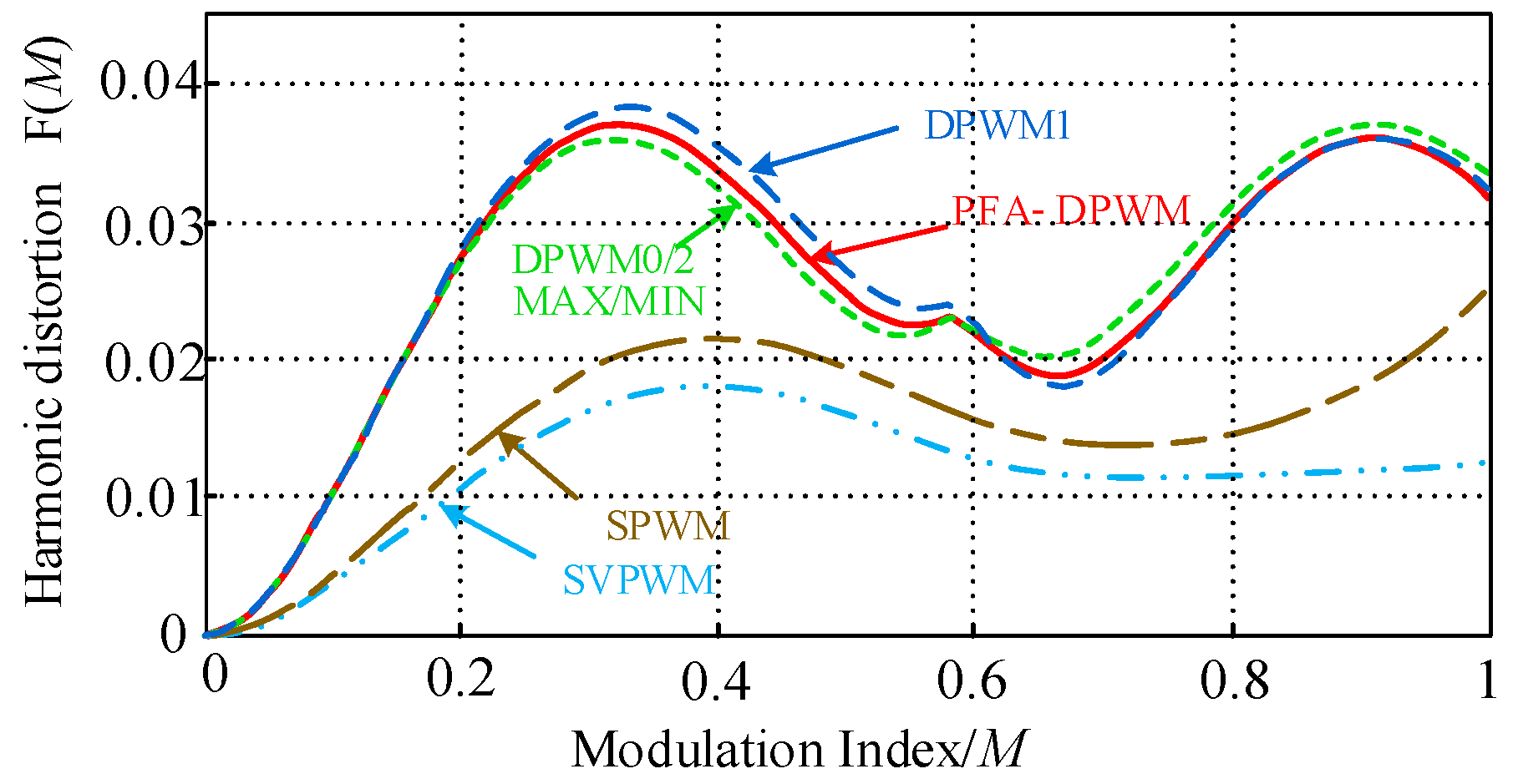
The harmonic distortion curves for different PWM strategies are plotted in Figure 8. The harmonic distortion function for the PFA-DPWM (φ = π/12) lies between those of DPWM0/2 and DPWM1. At low modulation indices, its harmonic performance is superior to that of DPWM1, while at high modulation indices, it surpasses DPWM0 and DPWM2.

4.2. Switching Losses

In high-power electronic systems, switching loss is also a critical parameter for evaluating the performance of DPWM strategies, as the device switching loss is proportional to the magnitude of the instantaneous load current. This section derives a mathematical model for the switching loss of a three-level DPWM over half a switching period and conducts a comparative analysis of the switching losses under different modulation strategies. For half a switching period, the PWM switching loss can be uniformly expressed as
P loss ( pwm ) = U e I m 1 π φ π + φ sin ( θ φ ) d θ
Therefore, the switching loss function of SVPWM can be derived as
P loss ( svpwm ) = 2 π U e I m
The switching loss function of DPWM0 is
P loss ( DPWM 0 ) ( φ ) = U e I m 2 π 0 π 2 sin ( θ φ ) d θ + 5 π 6 π sin ( θ φ ) d θ
The switching loss function of DPWM2 is
P loss ( DPWM 2 ) ( φ ) = U e I m 2 π 0 π 6 sin ( θ φ ) d θ + π 2 π sin ( θ φ ) d θ
The calculation for other DPWM strategies is similar, and it is only necessary to consider that different types of DPWM strategies have different switch clamping intervals.
The resulting simplified mathematical model for the three-level PFA-DPWM is
P loss ( PFA - DPWM ) ( φ ) = P loss ( DPWM 2 ) ( φ ) ( φ < - π 6 ) 1 2 ( - π 6 < φ < π 6 ) P loss ( DPWM 0 ) ( φ ) ( φ > π 6 )
The proposed three-level PFA-DPWM control strategy adaptively tracks the variation in the load power factor angle φ, ensuring the switching devices are clamped for one-third of the fundamental period, an interval aligned with the peak of the phase current. Theoretical derivation shows that the strategy is equivalent to DPWM2 when φ < −π/6 and to DPWM0 when φ > π/6. In the range of −π/6 < φ < π/6, its operational behavior is contingent upon the load power factor angle. Using the switching loss of SVPWM as a baseline, a normalized loss function is defined in (28). The switching losses for different three-level DPWM strategies are compared in Figure 9.
P DPWMx ( φ ) = P loss ( DPWMx ) ( φ ) P loss ( SVPWM )
As illustrated in Figure 9, the PFA-DPWM strategy is equivalent to DPWM2 for φ < −π/6 and to DPWM0 for φ > π/6, while tracking the load power factor angle in the range of −π/6 < φ < π/6. As a result, the proposed three-level PFA-DPWM strategy effectively constructs the lower envelope of the switching losses among the compared strategies, thereby ensuring near-optimal efficiency across the entire power factor range.

4.3. Loss Model and Efficiency Analysis

The overall losses of an inverter predominantly consist of semiconductor device losses and magnetic component losses. To illustrate, the loss model for the T-type inverter operating under unity power factor conditions while employing the PFA-DPWM strategy.
The three-phase output current can be represented as
i a = I m cos ω t i b = I m cos ω t 2 π / 3 i c = I m cos ω t + 2 π / 3
Under dual-carrier modulation, the phase leg voltage exhibits two distinct states within each switching period: a non-zero level (positive or negative) and a zero level. This voltage level, in turn, dictates the conduction path of the phase current: for a non-zero voltage, the current is conducted by one of the outer switches, whereas for a zero voltage, it flows through a neutral-point switch and its corresponding anti-parallel diode. Assuming operation under unity power factor, the duty cycles for the non-zero and zero voltage levels are denoted as D±1 and D0, respectively:
D ± 1 = u a U M
D 0 = 1 u a U M
The conduction loss for phase A over one complete line-frequency cycle is given by
P cond = f g 0 1 / f g v CE 1 D ± 1 + v CE 0 D 0 + v D 0 D 0 i a t d t
where fg represents the line frequency (50 Hz). v CE 1 and v CE 0 are the on-state voltage drops of the outer and neutral-point switches, respectively, and v D 0 denotes the forward voltage drop of the neutral-point clamping diodes.
When the PFA-DPWM strategy is employed, the switches of a given phase leg remain inactive during one-third of the fundamental period. Throughout the remaining two-thirds of this period, the neutral-point switch and an outer switch each undergo one switching transition. Accordingly, the switching loss for a single-phase leg of the T-type inverter is formulated as
P sw = 2 f g n = 1 f s / ( 6 f g ) E on 1 n + E off 1 n + E rr 1 n + E on 0 n + E off 0 n + E rr 0 n + 2 f g n = f s / ( 3 f g ) f s / ( 2 f g ) E on 1 n + E off 1 n + E rr 1 n + E on 0 n + E off 0 n + E rr 0 n
where fs is the switching frequency. E on 1 n , E off 1 n , and E rr 1 n are the turn-on, turn-off, and reverse-recovery losses of the outer switches during the n-th switching period, respectively. E on 0 n , E o ff 0 n , and E rr 0 n represent the analogous loss components for the neutral-point switches.
The filter inductor loss PL, is primarily composed of copper and core losses, the values of which are typically obtained from the manufacturer’s specifications. Consequently, the total inverter loss is the summation of the conduction loss Pcond, switching loss Psw, and filter inductor loss PL, can be expressed as
P inv = 3 P cond + 3 P sw + 3 P L
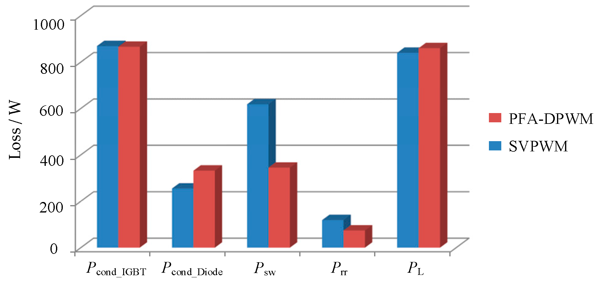
Figure 10 illustrates the loss distribution for a T-type inverter operating with the FPA-DPWM strategy, as calculated by the aforementioned loss model. Compared to the conventional SVPWM strategy, the FPA-DPWM approach achieves a notable reduction in Psw and Prr. While this approach incurs a slight increase in diode conduction loss, the overall inverter loss is nevertheless markedly diminished.

5. Simulation and Experimental Results

To verify the PFA-DPWM strategy, a T-type three-level circuit topology is depicted in Figure 11. The system parameters for the experimental setup are summarized in Table 5.

5.1. Simulation Results

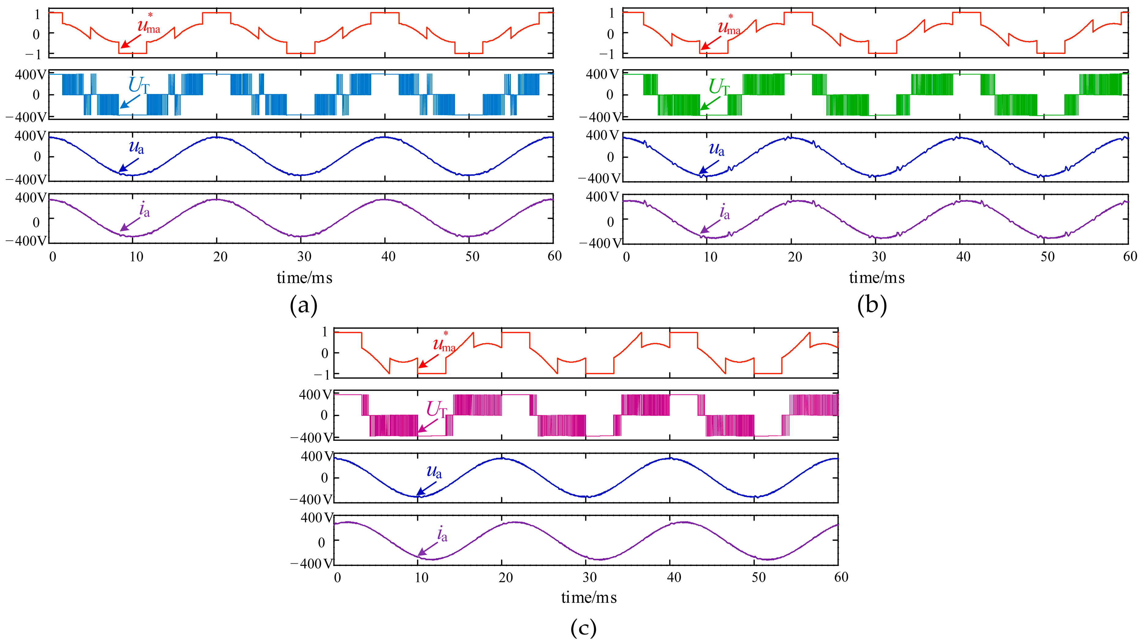
This paper uses MATLAB R2023b software for simulation. The simulated waveforms for the three-level inverter, operating under the proposed PFA-DPWM control strategy, are depicted in Figure 12. The analysis of these waveforms demonstrates that the PFA-DPWM algorithm dynamically identifies the phase interval corresponding to the peak absolute load current. Consequently, the power switches are clamped during this high-current interval, which substantially reduces the associated switching losses. Furthermore, the proposed three-level PFA-DPWM strategy demonstrates excellent voltage control performance.

5.2. Experimental Results

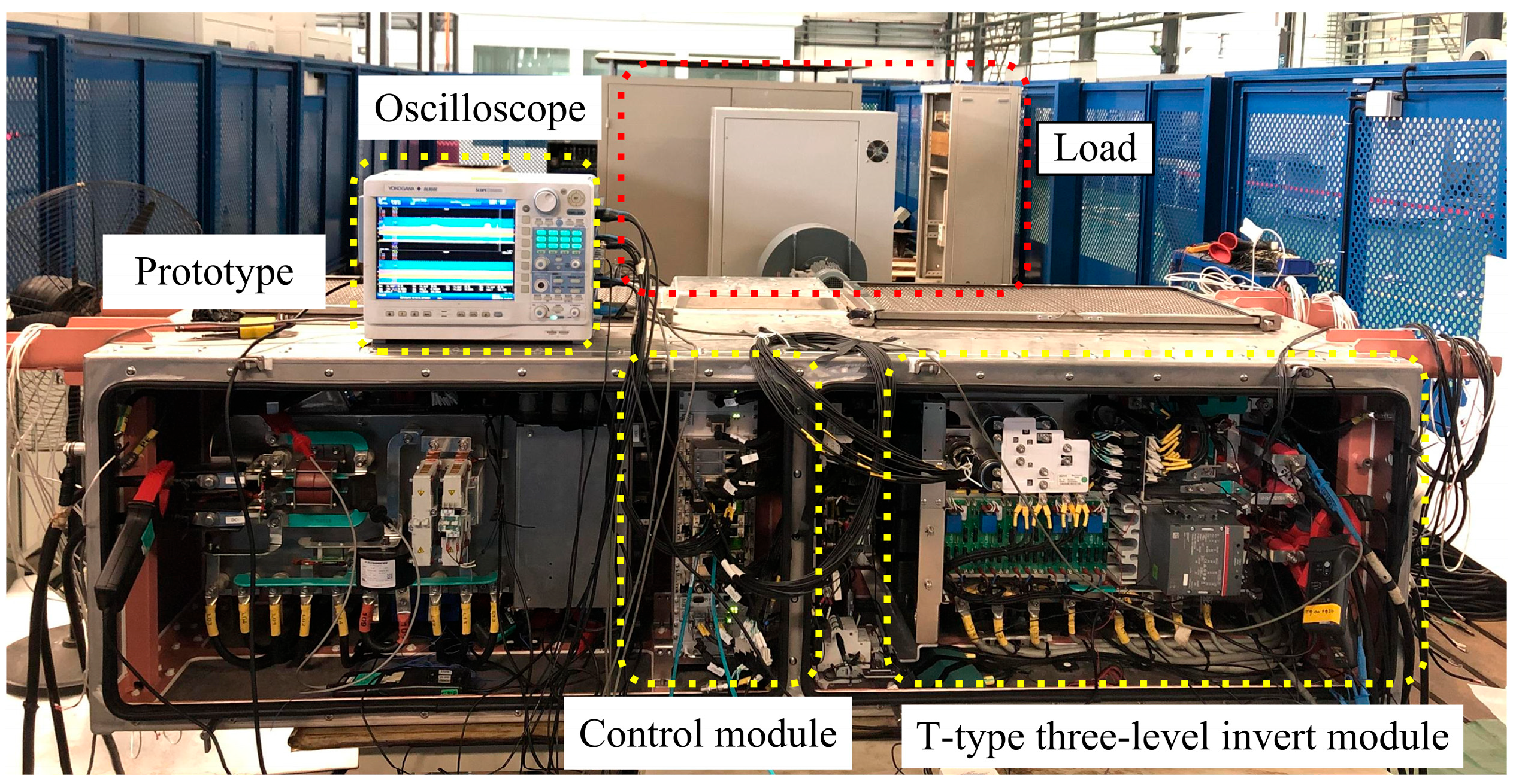
To verify the efficacy of the PFA-DPWM control strategy, an experimental platform for a 120 kVA T-type three-level inverter was established, as presented in Figure 13.
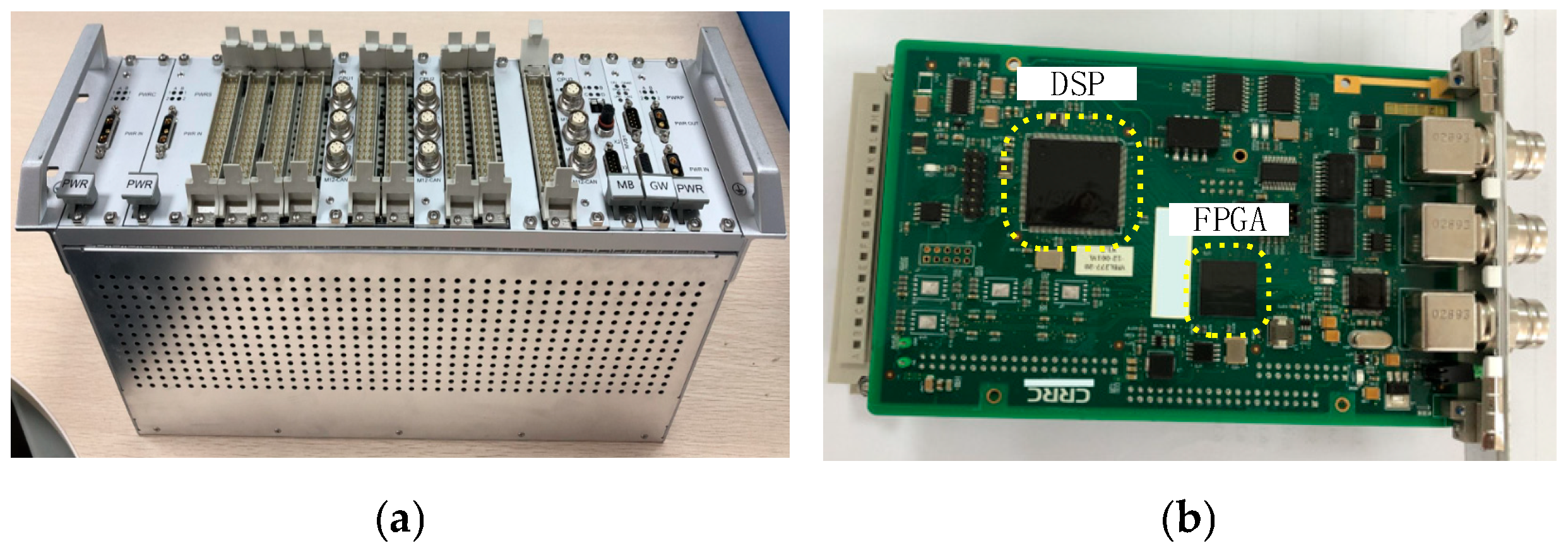
As shown in Figure 14, the integrated control unit is enclosed in a standard 3U chassis (Compliant with the 19-inch rack EIA-310 industrial standard).to suppress electromagnetic interference and enhance converter stability. Its core control board utilizes a Digital Signal Processor (DSP: TMS320F28335 Manufacturer: Texas Instruments, Dallas, TX, USA) and Field-Programmable Gate Array (FPGA: XC6SLX16-2FTG256I Manufacturer: Xilinx, San Jose, CA, USA) architecture.
Figure 15 and Figure 16 illustrate the steady-state experimental operational characteristics of the T-type inverter under half-load and full-load conditions, respectively. Under half-load (70 kW) and full-load (140 kW) operation, the measured THD of the line voltage uab is 2.07% and 1.82%, respectively, which demonstrates that the three-phase output voltage possesses excellent harmonic and steady-state characteristics.
Figure 17 illustrates the experimental waveforms of the T-type inverter under a transient load condition. When the load undergoes a step increase from 20 kW to 100 kW, the output line voltage uab exhibits a transient dip of approximately 65 V and recovers to its steady-state condition within 400 μs. This performance demonstrates the inverter’s fast dynamic response.
From Figure 18, the switching devices remain inactive for one-third of the fundamental period, centered around the interval where the phase current reaches its peak magnitude. In Figure 18b, the clamping interval of the phase-a PWM signal is shifted by φ = 30°, which aligns this interval with the peak of the phase current to achieve minimal switching losses. Simultaneously, the proposed PFA-DPWM strategy maintains favorable harmonic characteristics, and is demonstrated by the high-quality output waveforms.

6. Conclusions

This paper proposes a three-level power factor adaptive DPWM (PFA-DPWM) strategy developed for T-type inverters. A comprehensive analysis of the harmonic characteristics and switching losses is provided for various three-level DPWM strategies. The proposed PFA-DPWM consistently constructs the lower envelope of switching losses, achieving a reduction of up to 50% compared to conventional SVPWM. This is accomplished while maintaining low harmonic distortion, thereby striking a favorable balance between high efficiency and superior output quality.
Furthermore, a detailed analysis of different three-level carrier-based modulation schemes reveals that the line voltage THD for the PD scheme is significantly lower than that for the POD/APOD schemes, as its carrier harmonic common-mode components can be mutually canceled in the line voltages.
The simulation and experimental results confirm that the PFA-DPWM strategy successfully clamps the power switches during the one-third of the fundamental period aligned with the peak absolute load current, while also maintaining good harmonic performance for the three-level inverter output.

Author Contributions

Conceptualization, M.X. and Y.X.; methodology, M.X. and J.T.; software, J.T. and Z.L.; validation, J.T. and Y.Z.; formal analysis, M.X. and Y.X.; investigation, Y.Z.; resources, Y.X.; data curation, Z.L.; writing—original draft preparation, J.T.; writing—review and editing, M.X. and Y.X.; supervision, M.X.; project administration, M.X.; funding acquisition, M.X. All authors have read and agreed to the published version of the manuscript.

Funding

This research was funded by “the Fundamental Research Funds for the Provincial Universities of Liaoning, grant number LJ212410150040” and “the Natural Science Foundation of Liaoning Province, grant number 2025-BS-0448”.

Data Availability Statement

The data that support the findings of this study are available from the corresponding author upon reasonable request.

Conflicts of Interest

The authors declare no conflicts of interest.

Abbreviations

Symbols
ParametersDefinitions
udcDC bus voltage
MModulation index
u ma * ,   u mb * and u mc * Modulation signals of three-phase voltages
uzZero-sequence component
ua, ub, and ucOriginal phase voltages
φLoad power factor angle
u a ( φ ) , u b ( φ ) and u c ( φ ) Phase voltages after being phase-shifted by the φ
u mz ( φ ) Zero-sequence voltage of three-level PFA-DPWM
u ma * ( φ ) , u ma * ( φ ) , and u mc * ( φ ) Modulation voltages of three-level PFA-DPWM
fc/fmCarrier ratio
LσLine-to-line equivalent leakage inductance
exyThe average internal electromotive force of the load
Abbreviations
DPWMDiscontinuous pulse width modulation
SPWMSinusoidal pulse-width modulation
SVPWMSpace vector pulse-width modulation
PFAPower factor adaptive
PDPhase disposition
PODPhase opposition disposition
APODAlternative phase opposition disposition
NPNeutral point
ZSVZero-sequence voltage
THDTotal harmonic distortion
EMFElectromotive force
DSPDigital signal processor
FPGAField-programmable gate array

Appendix A

Considering the modulation index for SPWM, the mean square value of the total harmonic current is expressed by (A1) and(A2).
When M 3 / 3 , there is
I 2 xy , h , rms = 1 π π 6 5 π 6 Δ i x y 2 d θ = Δ T s 2 12 π ( U dc L σ ) 2 ( π 6 0 Δ i x y 2 d θ 0 > u x u y + 0 π 6 Δ i x y 2 d θ 1 + u y u x 0 > u y + π 6 π 2 Δ i x y 2 d θ 1 + u y u x 0 > u y + π 2 2 π 3 Δ i x y 2 d θ 1 + u y u x 0 > u y + 2 π 3 5 π 6 Δ i x y 2 d θ u x u y 0 ) = Δ T s 2 π ( U dc L σ ) 2 1 768 M 2 ( 72 ( - 3 + π ) + M ( 720 + 256 3 + 27 M ( 3 3 + 4 π ) )
When 0 M 3 / 3 , there is
I 2 xy , h , rms = 1 π π 6 5 π 6 Δ i x y 2 d θ = Δ T s 2 12 π ( U dc L σ ) 2 ( π 6 0 Δ i x y 2 d θ 0 > u x u y + 0 2 π 3 Δ i x y 2 d θ 1 + u y u x 0 > u y + 2 π 3 5 π 6 Δ i x y 2 d θ u x u y 0 ) = Δ T s 2 12 π ( U dc L σ ) 2 ( 4 π 3 3 4 M 2 3 + 4 3 2 M 3 + 9 π 8 M 4 )

References

  1. Alshahrani, S.; Khan, K.; Abido, M.; Khalid, M. Muhammad Khalid Grid-forming converter and stability aspects of renewable-based low-inertia power networks: Modern trends and challenges. Arab. J. Sci. Eng. 2024, 49, 6187–6216. [Google Scholar] [CrossRef]
  2. Liu, Z.; Sun, Y.; Ma, C. An overview of grid-forming technology and its application in new-type power system. Glob. Energy Interconnect. 2024, 7, 541–552. [Google Scholar] [CrossRef]
  3. Yang, Z.; Zeng, J.; Ren, Q.; Wu, L.; Liao, Z. A Semi Discontinuous PWM Method for Mitigating Oscillation in a Three-Level Grid-Tied PV Inverter. In Proceedings of the IEEE Energy Conversion Congress and Exposition (ECCE), Vancouver, BC, Canada, 10–14 October 2021. [Google Scholar] [CrossRef]
  4. Liu, Z.; Zheng, Z.; Sudhoff, S.; Gu, C.; Li, Y. Reduction of Common-Mode Voltage in Multiphase Two-Level Inverters Using SPWM with Phase-Shifted Carriers. IEEE Trans. Power Electron. 2016, 31, 6631–6645. [Google Scholar] [CrossRef]
  5. Yan, Q.; Zhou, Z.; Wu, M.; Yuan, X.; Zhao, R.; Xu, H. A Simplified Analytical Algorithm in abc Coordinate for the Three-Level SVPWM. IEEE Trans. Power Electron. 2021, 36, 3622–3627. [Google Scholar] [CrossRef]
  6. Srivastava, S.; Chaudhari, M.A. Comparison of SVPWM and SPWM Schemes for NPC Multilevel Inverter. In Proceedings of the IEEE International Students’ Conference on Electrical, Electronics and Computer Science (SCEECS), Bhopal, India, 22–23 February 2020. [Google Scholar] [CrossRef]
  7. Wen, X.; Yin, X.; Zhang, Z. Unified Space Vector PWM Implementation Method for Three-Phase Inverters. Trans. China Electrotech. Soc. 2009, 24, 87–93. [Google Scholar] [CrossRef]
  8. An, S.; Sun, X.; Chen, Y.; Zhong, Y.; Ren, B. A New Generalized Implementation Method of Discontinuous PWM. Proc. CSEE 2012, 32, 59–66. [Google Scholar]
  9. Ojo, O. The Generalized Discontinuous PWM Scheme for Three-Phase Voltage Source Inverters. IEEE Trans. Ind. Electron. 2004, 51, 1280–1289. [Google Scholar] [CrossRef]
  10. Li, K.; Wei, M.; Xie, C.; Deng, F.; Guerrero, J.; Vasquez, J. Triangle Carrier-Based DPWM for Three-Level NPC Inverters. IEEE J. Emerg. Sel. Top. Power Electron. 2018, 6, 1966–1978. [Google Scholar] [CrossRef]
  11. Song, X.; Tian, J.; Li, L.; Li, S.; Zheng, Y.; Zhang, F. A Carrier-Based DPWM for T-Type Three-Level Inverter with ZSV Injected by Searching Neutral Point Current. In Proceedings of the IEEE 2nd International Power Electronics and Application Symposium (PEAS), Guangzhou, China, 10–13 November 2023. [Google Scholar] [CrossRef]
  12. Xia, C.; Zhang, G.; Yan, Y.; Gu, X.; Shi, T.; He, X. Discontinuous Space Vector PWM Strategy of Neutral-Point-Clamped Three-Level Inverters for Output Current Ripple Reduction. IEEE Trans. Power Electron. 2017, 32, 5109–5121. [Google Scholar] [CrossRef]
  13. Jiang, W.; Jiang, H.; Liu, S.; Ji, S.; Wang, J. A Carrier-Based Discontinuous PWM Strategy for T-Type Three-Level Converter With Reduced Common Mode Voltage, Switching Loss, and Neutral Point Voltage Control. IEEE Trans. Power Electron. 2022, 37, 1761–1771. [Google Scholar] [CrossRef]
  14. Wang, J.; Ji, S.; Jiang, W.; Liu, S.; Jiang, H. A Novel Discontinuous PWM Strategy to Achieve Switching Loss Reduction and Neutral Point Voltage Balance for Vienna Rectifier. Proc. CSEE 2022, 42, 4125–4138. [Google Scholar] [CrossRef]
  15. Zou, Y.; Xing, Y.; Zhang, L.; Zheng, Z.; Liu, X.; Hu, H. Dynamic-Space-Vector Discontinuous PWM for Three-Phase Vienna Rectifiers with Unbalanced Neutral-Point Voltage. IEEE Trans. Power Electron. 2021, 36, 9015–9026. [Google Scholar] [CrossRef]
  16. Hossain, S.; Biswas, S.P.; Mondal, S.; Nath, J.; Islam, M.R. Advanced Voltage Balancing Discontinuous PWM Technique for Solar PV Fed Grid-Tied NPC Inverters. IEEE Trans. Appl. Supercond. 2024, 34, 1–5. [Google Scholar] [CrossRef]
  17. Yang, Z.; Zeng, J.; Ren, Q.; Wu, L.; Liao, Z. Research on Neutral-Point Balance Control of Three-Level Inverter Based on Hybrid DPWM. In Proceedings of the IEEE Conference on Industrial Electronics and Applications, Xi’an, China, 19–21 June 2019. [Google Scholar] [CrossRef]
  18. Zhao, M.; Chen, J.; Xin, Z.; Liu, H. A Hybrid DPWM Based Variable Switching Frequency Scheme for ZVS Three-Phase Three-Level Neutral-Point-Clamped Inverter. IEEE Trans. Ind. Electron. 2024, 71, 14276–14286. [Google Scholar] [CrossRef]
  19. Pham, K.D.; Nguyen, Q.V.; Nguyen, N.-V. PWM Strategy to Alleviate Common-Mode Voltage with Minimized Output Harmonic Distortion for Five-Level Cascaded H-Bridge Converters. Energies 2021, 14, 4476. [Google Scholar] [CrossRef]
  20. Busacca, A.; Di Tommaso, A.O.; Miceli, R.; Nevoloso, C.; Schettino, G.; Scaglione, G.; Viola, F.; Colak, I. Switching Frequency Effects on the Efficiency and Harmonic Distortion in a Three-Phase Five-Level CHBMI Prototype with Multicarrier PWM Schemes: Experimental Analysis. Energies 2022, 15, 586. [Google Scholar] [CrossRef]
  21. Zou, Y.; Zhang, L.; Xing, Y.; Zhuge, H.; Shen, X.; Zhang, Y. An Optimized DPWM With Reduced Leakage Current for Three-Phase Three-Level Inverters with Unbalanced Neutral-Point Voltage. IEEE Trans. Power Electron. 2024, 39, 16346–16360. [Google Scholar] [CrossRef]
  22. Hu, Z.; Xing, X.; Liu, C.; Zhang, R.; Blaabjerg, F. A Modified Discontinuous PWM Method for Three-Level Inverters with the Improved LCL Filter. IEEE Trans. Power Electron. 2024, 39, 5498–5509. [Google Scholar] [CrossRef]
  23. Zhang, Y.; Li, C.; Schutten, M.; De Leon, C.F.; Prabhakaran, S. Common-Mode EMI Comparison of SPWM, DPWM, and SVPWM Modulation Approaches. In Proceedings of the IEEE Energy Conversion Congress and Exposition, Baltimore, MD, USA, 29 September–3 October 2019. [Google Scholar] [CrossRef]
  24. An, S.; Sun, X.; Zhong, Y.; Matsui, M. Research on a new and generalized method of discontinuous PWM strategies to minimize the switching loss. In Proceedings of the IEEE PES Innovative Smart Grid Technologies, Tianjin, China, 21–24 May 2012. [Google Scholar] [CrossRef]
  25. Addin, A.S.; Sahan, B.; Brueckner, T. Comparison of Different PWM Methods Assuming Equal Harmonic Loss Conditions. In Proceedings of the PCIM International Exhibition and Conference for Power Electronics, Intelligent Motion, Renewable Energy and Energy Management, Online, 3–7 May 2021. [Google Scholar]
  26. Wang, M.; Xu, L.; Yang, B.; Li, J.; Gu, C.; Zhang, H. Optimized Carrier Disposition Based Discontinuous Pulse-width Modulation Method for three-level NPC Converters. In Proceedings of the IEEE Energy Conversion Congress and Exposition, Baltimore, MD, USA, 29 September–3 October 2019. [Google Scholar] [CrossRef]
  27. Shin, H.; Lee, K.; Choi, J.; Seo, S.; Lee, J. Power loss comparison with different PWM methods for 3L-NPC inverter and 3L-T type inverter. In Proceedings of the International Power Electronics and Application Conference and Exposition, Shanghai, China, 5–8 November 2014. [Google Scholar] [CrossRef]
  28. Xu, M.; Li, C.; Wang, Z.; Ge, Y.; Li, G.; Wang, N. DPWM Control Strategy of Auxiliary Inverter for Urban Rail Transit Based on Adaptive Power Factor. Proc. CSEE 2021, 41, 356–365. [Google Scholar] [CrossRef]
  29. Holmes, D.G.; Lipo, T.A. Pulse Width Modulation for Power Converters: Principles and Practice; John Wiley & Sons: Hoboken, NJ, USA, 2003; pp. 453–484. [Google Scholar]
  30. Ali Iftekhar, M.; Tafti, H. Advanced Multilevel Converters and Applications in Grid Integration; John Wiley & Sons: Hoboken, NJ, USA, 2018; pp. 243–254. [Google Scholar]
  31. Wu, W.-J.; Hu, L.-D.; Xin, Z.-Y.; Guo, C. Modeling and Analysis of Voltage Harmonic for Three-Level Neutral-Point-Clamped H-Bridge Inverter Considering Dead-Time. Energies 2022, 15, 5937. [Google Scholar] [CrossRef]
Figure 1. Topology diagram of a T-type three-level inverter.
Energies 18 04574 g001
Figure 2. (a) Distribution of space vectors, (b) a phase voltage reference vector in sub-sector 5 of Sector I. (The arrows represent the different voltage vectors and the numbers represent the different sectors).
Energies 18 04574 g002
Figure 3. Simulation waveform of load power factor angle φ = π/12 for different DPWM strategies: (a) DPWM1; (b) DPWM0; (c) PFA-DPWM.
Energies 18 04574 g003
Figure 4. Common triangular carrier-based modulation schemes: (a) PD modulation (b) POD/APOD modulation.
Energies 18 04574 g004
Figure 5. Phase-a voltage spectrum when M = 0.8, fc/fm = 50: (a) PD modulation; (b) POD/APOD modulation.
Energies 18 04574 g005
Figure 6. ab line voltage spectrum when M = 0.8, fc/fm = 50: (a) PD modulation; (b) POD/APOD modulation.
Energies 18 04574 g006
Figure 7. Switch status in the carrier period at exy > 0: (a) 0 > ux > uy; (b) ux > uy > 0; (c) ux > 0 > uy, uxuy > 1; (d) ux > 0 > uy, uxuy < 1.
Energies 18 04574 g007
Figure 8. Comparison of harmonic distortion in different PWM.
Energies 18 04574 g008
Figure 9. Comparison of switching loss of different PWM strategies.
Energies 18 04574 g009
Figure 10. Comparison of loss distribution between SVPWM and PFA-DPWM.
Energies 18 04574 g010
Figure 11. T-type three-level inverter topology.
Energies 18 04574 g011
Figure 12. Simulation waveform of three-level PFA-DPWM algorithm for different load power factor angle φ: (a) φ = 0; (b) φ = π/12; (c) φ = π/6.
Energies 18 04574 g012
Figure 13. Experimental test platform for T-type three-level inverter.
Energies 18 04574 g013
Figure 14. Diagram of control cabinet and core control board: (a) control cabinet; (b) core control board.
Energies 18 04574 g014
Figure 15. Waveform of T-type three-level inverter at half load (70 kW).
Energies 18 04574 g015
Figure 16. Waveform of T-type three-level inverter at full load (140 kW).
Energies 18 04574 g016
Figure 17. Waveform of T-type three-level inverter under a transient load condition.
Energies 18 04574 g017
Figure 18. Experimental waveforms of three-level PFA-DPWM: (a) φ = 0°, (b) φ = 30°.
Energies 18 04574 g018
Table 1. Carrier functions fc+(x), fc−(x) and modulating function fm(y).
f c + ( x ) f c ( x ) f m ( y )
PD x π 0 < x π x π π x 0 1 + x π 0 < x π 1 x π π x 0 M cos y
POD/APOD x π 0 < x π x π π x 0 x π 0 < x π x π π x 0 M cos y
Table 2. Phase voltage switching function fPD(x, y) for PD modulation.
f PD ( x , y ) π x 0 0 < x π
V dc 2 M cos y > x π M cos y > x π
0 x π > M cos y > 1 x π x π > M cos y > 1 + x π
V dc 2 M cosy < 1 x π M cosy < 1 + x π
Table 3. Phase voltage switching function fPOD/APOD(x, y) for POD/APOD modulation.
f POD / APOD ( x , y ) π x 0 0 < x π
V dc 2 M cos y > x π M cos y > x π
0 x π > M cos y > x π x π > M cos y > x π
V dc 2 M cos y < x π M cos y < x π
Table 4. Mean square value of current ripple for various switching state combinations.
ConditionsT1, T2, T3RMS of Current Ripple
0 > u x > u y T 1 = ( 1 + u y ) Δ T / 2
T 2 = ( u x u y ) Δ T / 2
T 3 = u x Δ T / 2
Δ i x y 2 = V dc L σ 2 Δ T 2 12 ( u x u y ) 2 [ u x 2 + u x ( 1 + u y ) + ( 1 + u y ) 2 ]
u x > u y > 0 T 1 = u y Δ T / 2
T 2 = ( u x u y ) Δ T / 2
T 3 = ( 1 u x ) Δ T / 2
Δ i x y 2 = V dc L σ 2 Δ T 2 12 ( u x u y ) 2 [ ( u x 1 ) 2 +   ( u x 1 ) u y + u y 2 ]
u x > 0 > u y , u x u y > 1 T 1 = ( 1 + u y ) Δ T / 2
T 2 = ( u x u y 1 ) Δ T / 2
T 3 = ( 1 u x ) Δ T / 2
Δ i x y 2 = V dc L σ 2 Δ T 2 12 ( 1 + u x u y ) 2 ( 1 u x + u x 2 + u y + u x u y + u y 2 )
u x > 0 > u y , u x u y < 1 T 1 = u x Δ T / 2
T 2 = ( 1 u x + u y ) Δ T / 2
T 3 = u y Δ T / 2
Δ i x y 2 = V dc L σ 2 Δ T 2 12 ( 1 u x + u y ) 2 ( u x 2 + u x u y + u y 2 )
Table 5. Parameters of the system.
ParametersValue
DC bus voltage750 VDC
Three-phase output voltage380 VAC
Rated power120 kVA
Switching frequency8 kHz
Output frequency50 Hz
Three-phase filter inductor40 μH
Three-phase filter capacitor20 μF
Disclaimer/Publisher’s Note: The statements, opinions and data contained in all publications are solely those of the individual author(s) and contributor(s) and not of MDPI and/or the editor(s). MDPI and/or the editor(s) disclaim responsibility for any injury to people or property resulting from any ideas, methods, instructions or products referred to in the content.