Review

Cadmium-Free Buffer Layer Materials for Kesterite Thin-Film Solar Cells: An Overview

by
Nafees Ahmad
1,* and
Guangbao Wu
2,*
1
College of Chemistry and Chemical Engineering, Central South University, Changsha 410083, China
2
School of Materials Science and Engineering, Nanjing University of Posts and Telecommunications, Nanjing 210023, China
*
Authors to whom correspondence should be addressed.
Energies 2025, 18(12), 3198; https://doi.org/10.3390/en18123198
Submission received: 14 May 2025 / Revised: 12 June 2025 / Accepted: 17 June 2025 / Published: 18 June 2025

Abstract

:
Kesterite (CZTS/CZTSSe) thin-film solar cells are considered an eco-friendly, earth-abundant, and low-cost photovoltaic technology that can fulfill our future energy needs. Due to its outstanding properties including tunable bandgap and high absorption coefficient, the power conversion efficiency (PCE) has reached over 14%. However, toxic cadmium sulfide (CdS) is commonly used as an n-type buffer layer in kesterite thin-film solar cells (KTFSCs) to form a better p–n junction with the p-type CZTS/CZTSSe absorber. In addition to its toxicity, the CdS buffer layer shows parasitic absorption at low wavelengths (400–500 nm) owing to its low bandgap (2.4 eV). For the last few years, several efforts have been made to substitute CdS with an eco-friendly, Cd-free, cost-effective buffer layer with alternative large-bandgap materials such as ZnSnO, Zn (O, S), In2Se3, ZnS, ZnMgO, and TiO2, which showed significant advances. Herein, we summarize the key findings of the research community using a Cd-free buffer layer in KTFSCs to provide a current scenario for future work motivating researchers to design new materials and strategies to achieve higher performance.

1. Introduction

Thin-film photovoltaic (PV) technology has huge potential to reduce the energy crisis of the 21st century. Although silicon (c-Si), cadmium telluride (CdTe), and copper–indium–gallium–sulfide (CIGS) are commercialized technologies, the higher processing cost of Si, the toxicity of cadmium (Cd), and the scarcity of indium and telluride are the main drawbacks that restrict their future application at a commercialized scale [1,2,3]. Therefore, earth-abundant, non-toxic kesterite (CZT(S, Se) has huge potential to replace all commercialized thin-film photovoltaic technology due to its outstanding properties such as high absorption coefficient (104 cm−1) and tunable bandgap (1.1–1.5 eV) [4].
Compared to other semiconductor materials such as gallium arsenide (GaAs), quantum dots, graphene, silicon nanowires, molybdenum disulfide, and mxene [5,6,7,8], CZTS is an emerging photovoltaic material that possesses several advantages such as non-toxicity, earth-abundancy, and tunable optoelectronic properties. Therefore, comparable to other types of solar cells such as CIGS, perovskite, and CdTe, CZTS is highly cost-effective and sustainable [9,10,11]. Some main advantages are its compatibility with flexible substrates (polymers, thin metal foil that can be integrated with smart textiles, rollable displays, lightway power sources for Internet of Things (IoT) devices, and building-integrated photovoltaics [12,13,14]. Despite several challenges such as defect-based recombination and lower PCE, ongoing research can improve its performance and enhance its potential for scalable and low-cost fabrication for next-generation flexible and eco-friendly energy applications. In addition, kesterite possesses versatile properties that can be suitable for emerging applications such as photodetectors, sensors, hydrogen evolution catalysis, photochemical cells, radiation detection, and thermoelectric devices.
The predicted Shockley–Queisser (S–Q) limit for kesterite thin-film solar is 32.2%. Currently, the PCE of KTFSCs has just reached 14.9% due to significant efforts by several research groups in different domains of kesterite thin-film technology [15,16]. The lower performance of KTFSCs is mainly due to a high voltage deficit or low open-circuit voltage (Voc) [17]. It has been investigated that several factors influence the device performance; for example, (1) formation of secondary phases such as Cu2S, Cu2SnS3, ZnS, and SnS2 with pure CZT(S, Se), (2) antisite defects (CuZn, SnZn, CuSn), defect complexes (VCu + ZnCu, ZnSn + 2ZnCu), and vacancies (VZn, VCu, VSn), (3) the unfavorable energy alignment at the CZT(S, Se)/CdS interface, and (4) the formation of thick MoSe2 at the back interface, which impedes the holes from the absorber layer towards the back interface [18].
Currently, cadmium sulfide (CdS) is used as a standard buffer material in KTFSCs [19]. However, Cd is a toxic and hazardous material that causes severe health and environmental issues [20]. Additionally, its narrow bandgap (~2.4 eV) significantly reduces the photon flux in the UV range [21]. In addition, the high lattice mismatch between kesterite and CdS generates interfacial defects, which limit the PV performance [22]. Therefore, finding alternate Cd-free buffer layer materials to replace CdS has become a hot research area.
Several Cd-free buffer layer materials such as ZTO, Zn (O, S), In2S3, ZnS, ZnMgO, and TiO2 have been employed in kesterite thin-film solar cells for the last few years [23,24,25,26]. In this contribution, we review the recent advancement in Cd-free buffer layer materials for KTFSCs. We compare the performance of Cd-free and CdS-based solar cells using different deposition techniques. The key issues of Cd-free buffer layer materials and the suitable process of deposition of the buffer layer, unfavorable band alignment, interface defects, and structural inhomogeneity are discussed. The interface concern at Cd-free/kesterite thin-film solar cells is still not a high priority among researchers. This work also highlights the challenges in the advances of Cd-free buffer layer materials to allow readers to fully understand the current scenario and what could be the best buffer layer material in the future to achieve a higher PCE using eco-friendly materials. Although kesterite solar cells have been broadly reviewed in terms of the absorber layer, device PCE limitations, and optimization strategies, the focus on a Cd-free buffer layer has not yet been explored effectively. The current advances on Cd-free material selection for the interface layer were overlooked in the prior literature. In this review, we discuss the interface of CdS/CZT (S, Se) and the type of hetero-interface (cliff and spike). Afterward, we explain Cd-free buffer layer materials such as ZTO, Zn (O, S), In2S3, ZnS, ZnMgO, and TiO2 in KTFSCs with a detailed discussion on the key issues of Cd-free buffer layer materials and the suitable process of deposition of the buffer layer, band alignment, interface defects, structural inhomogeneity, and performance. The summary and future perspectives are also presented at the end of this review.

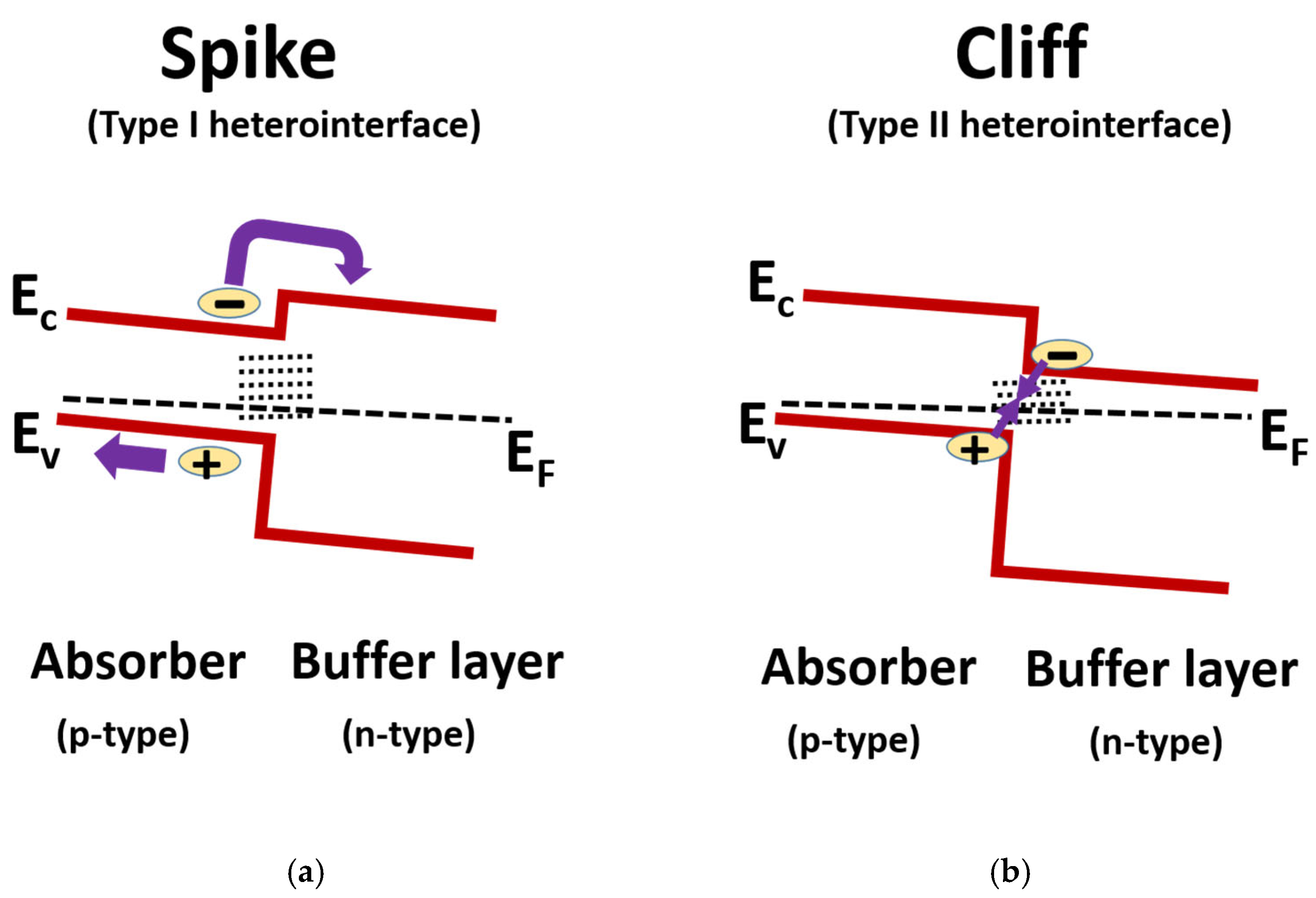
2. CdS/CZT (S, Se) Interface

CdS is widely employed as a buffer layer in KTFSCs. The chemical bath deposition (CBD) method is commonly adopted for CdS coating on top of the CZT (S, Se) film. As shown in Figure 1, two possible energy level offsets (i.e., spike-like and cliff-like) arise at the CZT(S, Se)/CdS junction [27]. In spike-like alignment, the conduction band (CB) of CdS lies below the CB of CZT (S, Se). In the case of cliff-like alignment, the CB of CdS is positioned above the CB of the absorber. For optimal carrier extraction, a “spike-like” offset with a conduction band offset (CBO) range between +0.1 and 0.3 eV is considered a suitable alignment at the interface. An unfavorable “cliff-like” alignment narrows the interface bandgap, which promotes the recombination process at the p–n junction [28]. According to theoretical calculations, a cliff-like alignment limits open-circuit voltage and fill factor by increasing the charge recombination at the interface [14].
Several reports have been published on the investigation of the CZT(S, Se)/CdS interface to understand the mechanism and factors responsible for the lower Voc in the device. These factors include the formation of secondary phases such as Cu2S, ZnS, and Cu2SnS3 in the bulk or at the absorbed/CdS interface, as well as defects and defect complexes like vacancies, antisites, and extended defects at CZT(S, Se)/CdS interfaces [4,29]. During the deposition of CdS, the intermixing of elements at the interface of CZT(S, Se)/CdS is also a key factor that strongly affects the performance of the final devices [4,30,31,32]. CdS is still a standard material in KTFSCs despite its parasitic absorption at low wavelengths (400–500 nm), toxicity, and non-optimal band alignment with CZT(S, Se) [33]. The chemical bath deposition (CBD) method is commonly used for CdS fabrication, where the substrate is dipped at 80 °C in cadmium salt, thiourea, and ammonia solution until the desired thickness is achieved. A champion PCE of 11.4% and 14.9% PCE have been reported in CdS/CZTS and CdS/CZTSSe thin-film solar cells, where CdS thickness was between 25 and 75 nm [21]. For future applications, it is urgently required to focus on eco-friendly and non-toxic Cd-free buffer layer materials because it is more important to make this technology at the commercial level. In addition, the machine learning (ML)-based approach has attracted considerable attention due to its use of very powerful predictive modeling to find materials for optoelectronic devices [34,35].

3. Cadmium-Free Buffer Layer

Due to the narrow bandgap (2.4 eV) and the toxic nature of CdS, different alternative buffer layers—for instance, Zn (O, S), ZnS (O, OH), ZnSnO, and ZnMgO—have been used in CIGS solar cells [36,37]. Similarly, different buffer layer materials have also been used in CZT(S, Se)-based devices. However, the maximum PCE was achieved in these devices with only the CdS buffer layer [2,15]. Unfortunately, until now researchers have not explored different buffer layer materials with a higher PCE than the CdS buffer layer for the last several years. Finding a Cd-free buffer layer with a higher performance is a hot topic for researchers. This section highlights the progress of different Cd-free buffer layers in KTFSCs.

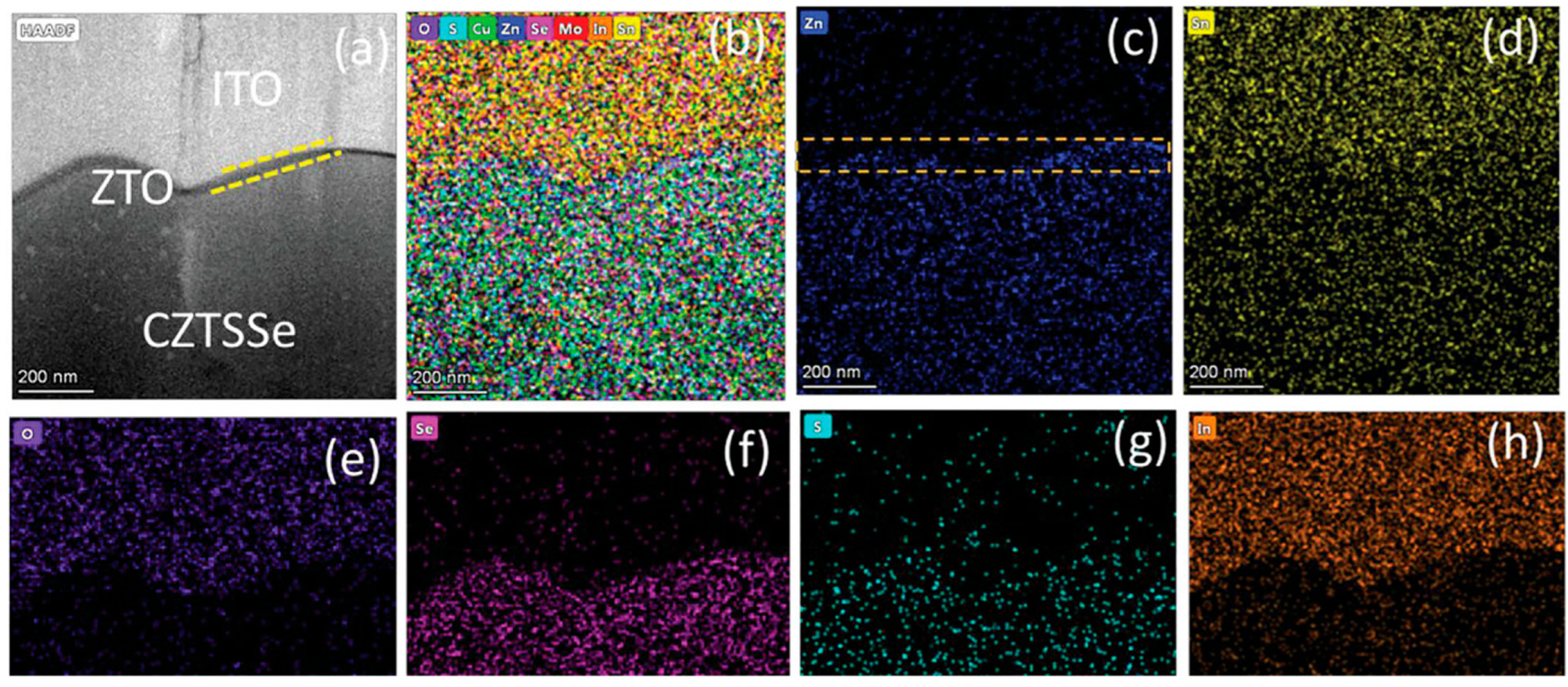
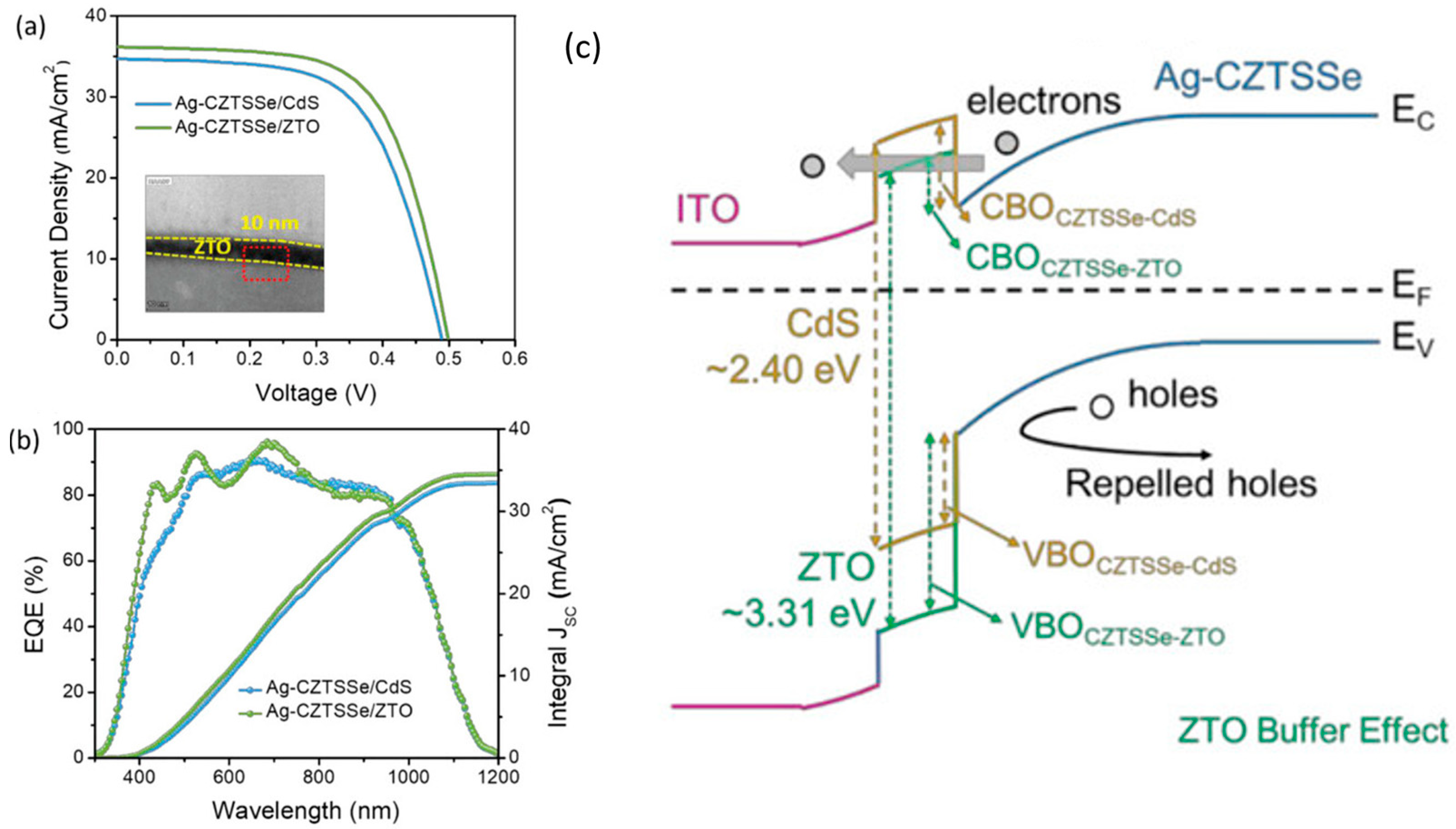
3.1. Zinc Tin Oxide (ZTO)-Based Buffer Layer
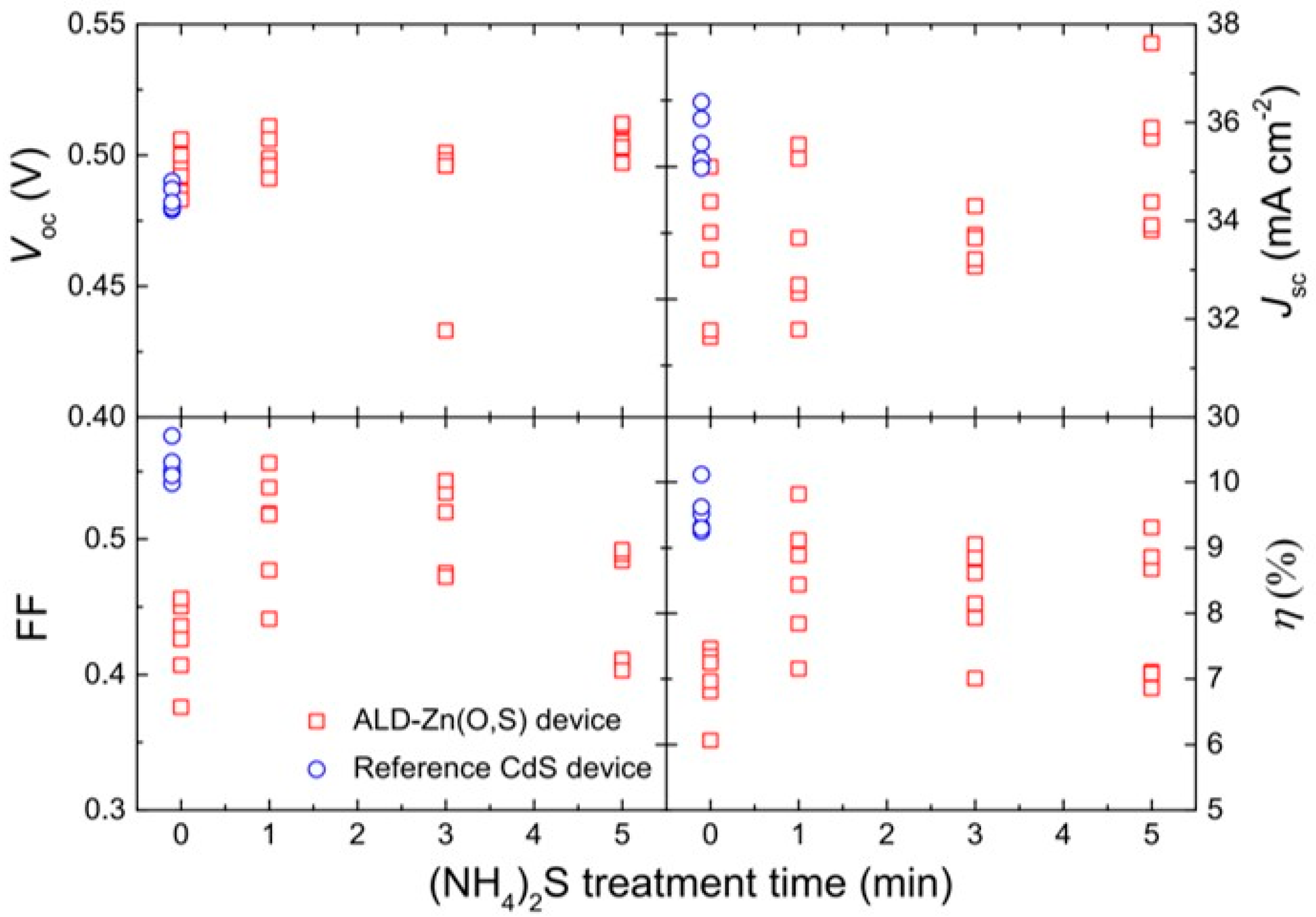
Zinc tin oxide (ZTO) as a Cd-free buffer layer has gained huge attention in kesterite thin-film photovoltaics due to its non-toxic nature and tunable wide bandgap with higher transparency [38,39,40]. Favorably, band alignment between ZTO and kesterite makes it more attractive for large-scale applications. ZTO has been used in CIGS thin-film solar cells as a Cd-free buffer layer since 2012 and delivers a promising PCE of over 18%. After the successful application in CIGS, kesterite photovoltaic researchers started to study the incorporation of ZTO into CZTS thin-film solar cells. Typically, sputtering and atomic layer deposition (ALD) techniques are the most common approaches to depositing a high-quality ZTO buffer layer. ALD is a more promising technique due to several advantages, such as homogeneity, control of stoichiometry, precise thickness control, and batch-to-batch uniformity compared to the CBD-processed CdS buffer layer. The demonstration of ALD-ZTO as a buffer layer in CZTSSe thin-film solar cells was first introduced by Li and co-workers (Table 1) [41]. They optimized the thickness of ZTO and the Zn-and-Sn ratio during the ALD process and found that optimizing the Zn-and-Sn ratio and thickness can have a huge impact on the device’s performance. They investigated that an extra-thin buffer layer cannot cover the whole surface of the CZTSSe film, which directly impacts p–n junction quality. On the other hand, a higher resistance in the case of an excessively thick ZTO buffer layer leads to severely reduce the fill factor (FF). The final device with an optimum thickness of 50 nm and Sn/(Sn + Zn) ratio of 0.167 delivered a PCE of 8.6%, which was higher than the reference device (8.1%) with a CdS buffer layer. This work motivated another researcher to further study the role of ZTO in kesterite thin-film solar cells.
Cui et al. [42] optimized the thickness and stoichiometry of an ALD-ZTO-based CZTSSe thin-film device. An extra-thin film of Zn(S, O) was also observed at the CZTS/ZTO interface, which acts as a hole barrier. Due to the well-matched band alignment between ZTO and CZTS, the ultra-thin Zn (S, O) film and sodium content in the ZTO-based device ultimately increased the Voc up to 10%, and the final device exhibited a higher PCE of 9.3% using a 10 nm ZTO layer. Ericson et al. [43] optimized the deposition temperature of ZTO to modify the band alignment with CZTS and the bandgap of the ZTO film. In this contribution, the deposition temperature of ZTO was kept at 105 °C, 145 °C, and 165 °C. Interestingly, the highest Voc and FF were achieved at 145 °C and 165 °C, respectively. The champion device in which ZTO had grown at 145 °C and a Sn/Sn + Zn ratio of 0.28 with a thickness of 10 nm exhibited a PCE of 9.0%. The better performance of the ZTO buffer layer was attributed to reduced charge recombination at the interface due to favorable band alignment between CZTS and the ZTO buffer layer, suggesting that ZTO could be a potential candidate for large-scale production in the future. Gubbo et al. [44] optimized the thickness and composition of the ALD-ZTO buffer layer. It was found that the i-ZnO window layer, which is normally deposited by the sputtering technique, is detrimental to the interface of CZTS/ZTO, which can change the stoichiometry and properties of the interfacial layer. It was found that the device with 30 nm thick ZTO and 2:1 ratio of Sn/Zn can effectively reduce charge recombination and prevent the interface defusion of i-ZnO and ZTO, leading to a higher PCE of 4% compared to a PCE of 3.9% in the CdS-based device.
The sputtering method has been used in several modern technological fields and has several advantages [45,46,47,48,49]. Lee et al. [50] studied the bandgap variation in ZTO at different deposition temperatures and various ratios of Sn(Zn + Sn) for ZTO obtained by the co-sputtering method. The composition of each component was controlled by varying the power applied to each sputtering target. Thanks to the wide bandgap of ZTO and the well-matched band alignment with CZTSSe, the optimum device delivered a champion PCE of 11.2%, which was higher than 9% for the Cd-based CZTSSe thin-film solar cells. During sputtering deposition techniques, the absorber layer is severely affected if the decomposition power is too high. On the other hand, low power increases the deposition time of the target materials. To overcome these issues, Grenet et al. [51] introduced a two-step processing method in which a thin low-power layer was deposited first, then a high-power thicker layer was fabricated on top of a thinner layer. Using this strategy, a higher PCE of 5.2% was achieved with the ZTO buffer layer than that of the CdS/CZTS-based device (4.6%). Lin and co-workers [52] introduced the bi-buffer layer concept by introducing ultra-thin CdS (10 nm) and ZTO (100 nm) through the co-sputtering method. It was revealed that ultra-thin CdS effectively works as a protection layer for the CZTSSe layer, while the ZTO layer reduces the interfacial recombination in flexible kesterite thin-film solar cells. Interestingly, the bi-buffer layer effectively reduced the interfacial charge recombination and promoted better band-to-band alignment at the interface, resulting in a higher PCE of 9.3%, which was superior to 8.5% (CdS-based device). Lee et al. [53] demonstrated that inserting an ultra-thin layer of ALD-Al2O3 between the buffer layer and the CZTS absorber layer can lead to variation in the surface and composition of the CZTS layer. It was revealed that trimethylaluminum (TMA) as a precursor of Al2O3, changes the surface and composition of CZTS, resulting in Cu-poor and Na-rich layers. Such surface/compositional modification leads to a wider bandgap and suppresses the defects at the p–n junction; thus, a champion PCE of 10.2% was realized.
Recently, ALD-based techniques have been used in several fields and gained huge attention [54,55,56,57]. Tajima et al. [58] investigated the performance of CZTS thin-film solar cells with an ALD-deposited ZTO buffer layer. The resulting devices exhibited an improved Jsc by 10% owing to reduced absorption at the shorter-wavelength region. The final device exhibited a higher performance of 5.7% with a ZTO buffer layer. Interestingly, a higher Voc of 0.81 V was achieved with a ZTO/CdS buffer bi-layer. Björkmanet et al. [59] investigated a Cd-free buffer layer based on ZTO at different deposition temperatures. It was found that ZTO processed at 95 °C delivered higher Voc and PCE compared to the CdS buffer layer. In addition, the ZTO process at 120 °C exhibited a similar PCE to the CdS buffer layer. The final PCE was measured to be 7.4% and 7.2% for the ZTO and CdS buffer layer in KTFSCs. Furthermore, Larsen et al. [60] used ZTO buffer layer in CZTS thin-film solar cells and achieved a PCE of 9.7%.
Recently, Ahmad et al. [61] explored that the device efficiency of CZTSSe can be improved by using a 10 nm thin layer of ALD-ZTO with a Zn: Sn ratio of (5:1) as shown in Figure 2. Firstly, they compared the performance of CZTSSe and Ag-doped CZTSSe devices. Secondly, different ratios of Zn: Sn and the thickness of ZTO were examined, and it was concluded that a 10 nm thin layer of ZTO effectively improves energy level alignment at the interface; thus, better p–n junction assists in boosting the Voc and FF of the device. The interface of CZTSSe-Ag/ZTO was further examined using high-resolution transmission electron microscopy (HRTEM) and TEM-EDS as shown in Figure 2a–h. The elemental distribution mapping clearly shows (Figure 2b–h) no impurity signals and only exhibits a tin-poor and zinc-rich interface, which also confirms that the interface is entirely composed of zinc, tin, and oxygen. In addition, the wide bandgap of ZTO helps to allow maximum light to the absorber, thus leading to a higher Jsc as shown in Figure 3. It was found that a small contact potential difference of the ZTO buffer layer facilitates the effective extraction of charge carriers. The final ZTO/Ag-CZTSSe-based device exhibited an 11.8% PCE, which was higher than the CdS/Ag-CZTSSe thin-film device (10.7%). To our knowledge, the achieved PCE (11.8%) represents the highest reported efficiency to date for Cd-free KTFSCs.
The ZTO buffer layer has been recognized as a potential candidate for KTFSCs but also faces major challenges. As discussed, Cd-free ZTO reduces the parasitic absorption and improves the current collection due to its wider bandgap. Additionally, it can form favorable CBO with the kesterite absorber upon suitable optimization, leading to a higher Voc by reducing charge carrier recombination at the interface. However, interface defects and recombination rates significantly reduce the FF and PCE compared to CdS buffer layer devices. As known, sputtering and ALD require precise control to assure reproducibility; therefore, ZTO performance is extremely sensitive to such deposition processes. Moreover, the PCE of ZTO-based devices has been improved; however, the overall performance is still behind CdS-based KTFSCs, which is mainly due to poor interface passivation. To overcome these issues, passivation layers such as the Al2O3, doping strategy (Ga, Mg), and ALD optimization could be beneficial.

3.2. Zn (O, S)

Several interface layer materials have been used in photovoltaic devices [62,63]. In the last decades, huge attention has been paid to the Zn (O, S)-based buffer layer due to its unique properties in KTFSCs [64,65,66,67]. Ericson et al. [68] investigated ALD-deposited Zn (O:S = 6:1) as a buffer layer in KTFSCs and achieved a PCE of 4.6% compared to 7.3. The lower PCE was ascribed to the reduced short circuit current and charge recombination at the photoactive layer/buffer layer. Grenet et al. [69] used the CBD method to deposit the ZnS(O, H) buffer layer on top of the CZTSSe film. The final device delivered a PCE of 5.8%. Moreover, Steierer and co-workers [70] deposited a Zn (O, S) buffer layer and introduced a double CBD approach using CZTSe as an active layer. They used two solvents (DMSO: water; only water) as a processing solvent to compare the performance of the corresponding buffer layer. Interestingly, DMSO, a water-processing device, exhibited a PCE over 5%, which was higher than 2% in water. The higher performance was attributed to the spike-type conduction band. Nguyen et al. [26] optimized the thickness of a ZnS thin film, which was deposited via the CBD method, and found that the device performance can be boosted by keeping the buffer layer thickness at the optimum value (25 nm). The final device delivered a PCE of 4.5%. It has been investigated that processing techniques have a huge impact on the final device performance. For example, Park et al. [71] optimized the thickness of ZnS using the CBD approach and achieved 3.8% PCE with 50 nm ZnS, while Kim et al. [72] achieved only 2% PCE using ZnS deposited by the sputtering method, with a thickness almost similar to the CBD method.
Jeong et al. [73] introduced a solution-based strategy to suppress the surface defects in order to enhance the surface properties of the ALD-Zn (O, S) buffer layer. Interestingly, the device based on Zn (O, S) exhibited a champion PCE of 9.8% after (NH4)2S treatment, which is comparable to a Cd-based device (10%). On the other hand, the device without (NH4)2S treatment showed a lower PCE of 7.5% in CZTSSe thin-film solar cells. To fully study the impact of NH4)2S, the device parameter of CZTSSe/Zn (O, S) was measured with and without (NH4)2S treatment. As shown in Figure 4, the device performance was improved significantly (7.46% to 9.82%) after one minute of (NH4)2S treatment, which is due to an improvement in FF. In addition, small changes in Voc (0.496 V and Jsc 35.6 mA/cm2) cannot be ignored. However, it was noticed that when further increasing the treatment time, FF was reduced slowly and finally exhibited low efficiency. The improved performance was ascribed to the elimination of the oxide layer and sulfur reduction.
Li et al. [74] improved the CZTSe-based device by ammonium etching and annealing treatment. The secondary phases of ZnO were removed as a result of the enhanced heterojunction quality of the CZTSSe/Z(O, S) interface, leading to a higher FF and lower series resistance. The final PCE of 7.2% was achieved using an anti-reflection coating comparable to the 8% efficiency of a Cd-based device. During the CBD, the concentration of thiourea significantly impacts the device’s performance. Neuschitzer et al. [75] explored the impact of thiourea concentration and light soaking on the final CZTSSe/ZnS(O, OH)-based device. A kink in the J–V curve was observed for the device with a thiourea concentration of 0.4–0.5 M, leading to an increased spike at the conduction band, resulting in a huge barrier at the interface, which reduces the photocurrent. However, after light soaking, the device exhibited much better performance. Moreover, the device that was treated with a 0.3 M solution of thiourea exhibited no impact of light soaking, and distortion in the J–V curve was observed; however, a reduction in Voc was noted. The resulting device showed a maximum PCE of 6.5% after light soaking and 0.4 M thiourea via the CBD route, which was similar to the reference device based on CdS with 6.9% PCE. Recently, Sanchez et al. [76] used the high-vapor-transport deposition method to deposit the Zn (O, S) film to improve the band alignment at the CZTSSe/Zn (O, S) heterojucntion. The investigation showed that the optimized ratio (0.5–0.7) of S/(S + O) led to an enhanced PCE of 6.8%, with an FF of 58.8%, Jsc of 20.3%, and Voc of 574 mV. The higher PCE was attributed to the spike-like CBO at the CZTSSe/buffer layer. Zhang et al. [77] used low-cost, environmentally friendly techniques, namely photochemical deposition (PCD) to fabricate Zn (O, S) thin-film solar cells and achieved a PCE of 3%. Similarly, Yang et al. [78] prepared a Cd-free Zn (O, S) buffer layer using sulfurization sputtering techniques. The findings showed that optimal sulfurization temperature reduced the traps, leading to suppressed charge recombination and improved transport properties. The final device with a Zn (O, S) buffer layer exhibited a final PCE of 5.1%, comparable to the control device with a CdS buffer layer processed via the CBD method.
Huang et al. [79] explored the impact of controlling precursor composition to enhance the quality of the interface between CZTS and Zn (O, S). The findings of this study demonstrated that depositing an SnS thin layer over CZTS created a CBO barrier of approximately 0.40 eV. The final device with a buffer layer based on Zn (O, S) exhibited a PCE of 7.2%. Steirer et al. [70] and Schnabel et al. [80] compared the performance of Zn (O, S) and CdS buffer layers in CZGSSe thin-film solar cells. The highest Voc of 730 meV was obtained in the case of the Zn (O, S) buffer layer due to the well-matched band alignment of Zn (O, S) with the absorbing layer. Jeong et al. [73] studied the impact of (NH4)2S on the photovoltaic properties of CZTSSe thin film using an ALD-Zn (O, S) buffer layer. It was revealed that (NH4)2S significantly improved the solar cell’s performance even after 60 s of treatment. The higher PCE was ascribed to the removal of oxides/hydroxides from the CZTSSe surface after treatment. Using Zn (O, S) as a buffer layer deposited with ALD processed at 90 °C, the final device exhibited a PCE of 9.8%. ZnMgO has also gained huge attention due to its ability to regulate CBO by changing the ratio of Mg/(Zn + Mg). For example, Hironiwa et al. [81] deposited ZnMgO by the co-sputtering method to examine the impact of Mg on CBO. ZnMgO with different bandgaps in the range of 3.5 eV–4.4 eV was obtained by varying the ratio of Mg/(Zn + Mg). The higher PCE was achieved with 3.76 eV using the ZnMgO buffer layer, which is attributed to better energy alignment at the ZnMgO/CZTS interface. However, work is rarely published regarding ZnMgO in KTFSCs.
Compared to the CdS buffer layer, Zn (O, S) enhances light flux, leading to a higher current density in resulting solar cells [82]. Additionally, the Cd-free composition also enhances its compatibility, which is well aligned with eco-friendly energy initiatives. However, studies show that the S ratio improves the CB alignment but introduces interface defects, whereas excessive ZnO increases recombination losses. Also, CBD of Zn (O, S) often leads to secondary phases and inhomogeneous film, which limits the Voc and FF. A hybrid buffer layer (ZnO/Zn (O, S) and post-deposition treatment could be effective approaches to mitigate these problems; however, reproducibility and stability will still remain a major challenge.

3.3. Indium Sulfide (In2S3)

Indium Sulfide (In2S3) is another non-toxic material with a moderate bandgap (2.1 eV). Some reports explored the positive CBO at the interface, which is a prerequisite to efficiently transport and extract the charge carrier the respective electrode. Jiang et al. [83] investigated CZTS interface doping using In2S3 induced by post-thermal annealing. It was found that rapid heat treatment facilitates In diffusion into the CZTS absorber at the interface region, leading to InSn defect formation as a result of p-type doping in the absorber layer. The final device based on CZTS/In2S3 exhibited 6.9% efficiency. These findings explore that the Voc of the device can be improved by In diffusion, which increases the built-in voltage across the p–n junction. Yan et al. [84] introduced a hybrid buffer layer based on In/Cd and achieved a PCE of 6.6%. The better performance was attributed to “spike-like” band alignment with CZTS and higher carrier concentration owing to In doping in the CZTS absorber. Mitzi et al. [85] also employed an In2S3/CdS hybrid layer using a CZTSSe absorber and reported a champion PCE of 12.7%. To minimize the Voc deficit, the carrier density needs to be further improved. Barkhouse et al. [86] deposited an In2S3 buffer layer by CBD and obtained a PCE of 7.1% in CZTSSe thin-film solar cells. A further improvement in PCE to 7.59% was observed after inserting an anti-reflection layer (MgF2). However, the CdS-based CZTSSe thin film showed a PCE of 7.5%. Furthermore, Khadka and Hiroi et al. [87] reported 5.7% and 6.3% PCEs in CZTS using the In2S3 buffer layer. Nevertheless, the authors did not provide any reference device in their experiments.
In2S3 is a non-toxic and thermally stable material with a tunable bandgap that effectively improves the interface quality and maintains favorable band alignment with a kesterite thin film that reduces optical losses and improves the performance of solar devices. However, secondary phases such as In(OH)3 and S vacancies cause interface defects, resulting in a lower Voc and FF. Importantly, the key issue is the reproducibility of the device performance, which is mainly due to sensitivity of the fabrication condition. It is required to focus on interface optimization strategies in order to compete with the conventional CdS buffer layer.

3.4. Titanium Dioxide (TiO2)

Titanium dioxide (TiO2) is a stable and non-toxic material with a bandgap of 3.8 eV, which is deposited using several approaches including sol–gel, the sputtering method, chemical vapor deposition (CVD), and ALD [88,89,90]. These methods allow for the precise control of the morphology and thickness of the buffer layer in solar devices [91,92]. TiO2 as a non-toxic buffer layer facilitates efficient charge separation and transport in KTFSCs due to suitable band alignment between TiO2 and the CZTSSe absorber [93,94,95]. Wang et al. [96] used the successive-ion-layer-adsorption-reaction (SILAR) deposition method to fabricate the CZTS absorber layer on the TiO2 nanorods as an ETL by adopting the superstrate configuration of the TCO/TiO2/interlayer/CZTS/Top contact. The findings of this contribution showed that the growth of CZTS nanocrystallites can be controlled by adjusting the SILAR cycles to achieve better photocurrent. It was also demonstrated that interfacial materials can effectively suppress charge recombination resulting in a higher Jsc and an internal quantum efficiency of over 60% in the low-wavelength region. However, the low Voc of 0.21 was ascribed to a downshift of the Fermi level of TiO2 after the deposition of the CZTS absorber layer.
Tseberlidis et al. [97] used the ALD method to deposit amorphous titania on top of the CZTS absorber layer using the substrate configuration Mo/CZTS/TiO2/AZO/Al. The final device after light soaking exhibited a PCE of 3.1% with a Jsc of 16 mA/cm2 and a Voc of 460 mV as shown in Figure 5. As is clearly shown in Figure 5b, the EQE of the devices ranges from 50% to 65% in the visible region, which is comparable to CdS-based devices. It was noted that the device with a 20 nm thick TiO2 buffer layer showed better performance. However, a slightly higher PCE was achieved in CdS-based devices. These promising results suggest that TiO2 can be a potential candidate to replace CdS in KTFSCs. Moreover, Wang et al. [96] adopted a superstrate configuration to address surface incompatibility by applying an Ag-refining step on ultra-thin Ag-CZTSSe with a TiO2 buffer layer. The refining step improved the Ag/(Cu + Ag) ratio and enlarged the grain size, thus boosting the charge transport. A champion PCE of 9.7% was achieved in CZTSSe thin film. However, the back surface defects were identified as the key limiting factors reducing the performance of solar cells. Dwivedi et al. [98] deposited a sulfurized sol–gel CZTS thin film, which showed excellent morphological and electrical properties using a superstrate configuration of ITO/ZnO/com-TiO2/Ag. Photovoltaic parameters were improved, yielding a Jsc of 4.7 mA/cm2 and a Voc of 0.40 V using a sulfurized sol–gel approach. Nisika et al. [99] used amorphous TiO2 with a bandgap of 3.8 eV to replace CdS in the CZTS device. The favorable “spike-like” alignment at the interface of CZTS/TiO2 with CBO of 0.17 eV was revealed by using ultraviolet photoelectron spectroscopy (UPS) and X-ray photoelectron spectroscopy (XPS) measurements. Moreover, the wider space charge region and higher electrical field at the CZTS/TiO2 heterojunction facilitate the separation of charge carriers.
TiO2 has shown excellent chemical stability, solution processibility, higher electron mobility, and lower parasitic absorption [100,101,102]. However, poor band alignment with CZTS/CZTSSe is a major issue, often leading to a cliff-like CBO that reduces the Voc due to the interface recombination of charge carriers. In addition, higher temperature processing and defect states severely reduce the device’s performance. A doping strategy (Nb, Y) can be an effective strategy to achieve competitive performance.
From a stability perspective, kesterite exhibits moderate but improvable stability, presenting its potential for large-scale commercialization. Moisture and oxygen are two important factors that can trigger the out-diffusion of S/Se and Cu migration, specifically along grain boundaries, while higher thermal stress accelerates cation disorders and promotes detrimental reactions with the adjacent buffer layer material [103,104,105,106]. Extended illumination activates the deep-level defects, particularly selenium vacancies (Vse) and copper antisite defects, resulting in a 6–10% PCE decline during >500 h of light exposure [32,107]. Interfacial stability is also still a major challenge; for example, Zn (O, S) forms secondary phases (ZnSe) that increase charge recombination, leading to lower device performance. Currently, CZTS/CZTSSe thin-film technology is still far behind CIGS technology; therefore, stable interfacial materials, a proper encapsulation strategy, and the quality of the absorber/interface issues could help to improve the stability of KTFSCs.
Table 1. Cd-free buffer layer materials and comparative performance with CdS in KTFSCs.
AbsorberBuffer
Layer
Deposition TechniqueVoc
(mV)
Jsc
(mA/cm2)
FF
(%)
PCE
(%)
Ref.
CZTSSeZTOALD714.034.161.08.6[41]
CdSCBD404.032.560.48.1
CZTSZTOALD720.020.464.09.3[42]
CdSCBD65216.564.26.9
CZTSZTOALD679.021.661.09.0[43]
CdSCBD608.020.558.07.2
CZTSSeZTOALD445.036.369.011.2[50]
CdSCBD---9.0
CZTSZTOSputtering721.014.051.05.2[51]
CdSCBD615.012.958.34.6
CZTSSeZTO/CdS-44836.758.79.3[52]
CdSCBD41934.669.08.5
CZTSZTOALD736.022.066.010.2[53]
CdSCBD652.016.569.06.9
CZTSZTOALD630.018.749.05.7[58]
CdSCBD660.017.062.07.0
CZTSZTOALD682.217.960.07.4[59]
CdSCBD666.019.455.67.2
CZTSZTOALD746.019.168.09.7[60]
CdSCBD809.017.061.28.4
Ag-CZTSSeZTOALD498.036.266.5311.8[61]
CdSCBD490.034.092.910.7
CZTSZn (O, S)ALD482.017.255.54.6[68]
CdSCBD652.017.563.87.3
CZTSSeZn (O, S)CBD376.029.052.05.8[69]
CdSCBD389.034.055.07.0
CZTSSeZn (O, S)CBD336.025.051.05.0[70]
CdSCBD---8.0
CZTSSeZnSCBD596.015.449.14.5[26]
CdSCBD640.015.448.54.7
CZTSSeZnSCBD309.023.554.03.8[71]
CdSSputtering362.024.060.05.2
CZTSZnSCBD311.012.155.72.1[72]
CdSALD561.018.448.24.9
CZTSSeZn (O, S)CBD49635.656.09.8[73]
CBDCBD48236.458.010.1
CZTSSeZn (O, S)CBD35833.5607.2[74]
Zn (O, S)CBD38835.9588.0
CZTSSeZnS(O,OH)CBD33232.651.85.6[75]
CdS 40130.556.36.9
CZTSZn (O, S)PCD516.016.835.33.0[77]
CdSCBD---4.3
CZTSZnO, Zn (O, S)Sulfurization610.121.140.05.1[78]
CdSCBD---5.0
CZTSZn (O, S)CBD708.019.254.07.2[79]
CdSCBD----
CZGSSeZn (O, S)Sputtering730.013.048.04.6[80]
CdS----6.0
CZTSSeZn (O, S)ALD496.035.656.09.8[73]
CdSCBD---10.1
CZTSIn2Se3CBD6212054.56.9[83]
CdSCBD7051863.28.1
In2Se3CBD42432.355.07.5[86]
CdSCBD46527.162.17.7
CZTSeIn2Se3CSP431.028.347.15.7[87]
CdSCBD----
CZTSSeTiO2Sputtering490.031.463.09.7[96]
CdSCBD----
CZTSTiO2ALD47617.444.03.71[97]
CdSCBD55516.159.74.14

4. Summary and Outlook

Herein, Cd-free buffer layer materials in CZTS/CZTSSe solar cells are reviewed. Charge carrier recombination at interfaces due to lattice mismatch, band offset, the diffusion of secondary phases, and the issues of charge extraction and recombination have been evaluated using a Cd-free buffer layer. Among them, ALD-ZTO was demonstrated to be an efficient buffer layer, showing a higher PCE approaching 12% in CZTSSe thin-film solar cells due to its wider bandgap (3.5–3.7) and spike-like alignment with the CZTSSe absorber—thanks to the ALD process, which can precisely control the stoichiometry and thickness of the buffer layer. On the other hand, the Zn (O, S) family showed better performance only with a lower-bandgap CZTSSe absorber. In2Se3 exhibited some promising results comparable to the CdS buffer layer; however, indium is an expensive element, which makes it less attractive for large-scale applications. TiO2 has shown better buffer layer properties and can be used as an alternative layer. Finding a Cd-free buffer layer comprises some important steps that include a theoretical approach, experimental work, and an advanced characterization technique. The current efforts of a Cd-free buffer layer are mostly composed of introducing a passivation layer or proposing heat treatment strategies, which cannot solve the key issue of Cd-free buffer layers. In Cd-free buffer layer materials, interface defects such as S vacancies, secondary phases, and poor band alignment are the key issues limiting the Voc and FF of the devices. Furthermore, the poor reproducibility of thin-film devices often arises due to CBD and the sputtering process. Additionally, the thermal and environmental stability of some materials are lower; for instance, Zn (O, S) undergoes degradation upon heat and illumination.
For future Cd-free buffer layer materials, efforts are expected to be focused on but not limited to the following directions:
  • It is urgently required to focus on new, cost-effective, Cd-free buffer layer materials, such as multiple metal oxides and sulfides, which could be an efficient alternative to boost the performance of KTFSCs. Additionally, heterojunction designs such as hybrid organic–inorganic buffer materials could be employed.
  • The integration of kesterite with tandem and emerging photovoltaic technologies can boost the PCE beyond 20%; for example, kesterite–perovskite tandem solar devices and optimized flexible buffer layers for wearable applications.
  • Investigating a self-healing photoactive passivation layer that dynamically mitigates defects under light will be highly favorable.
  • The machine learning model is an efficient route to select suitable candidates with an optimal energy level alignment, wider bandgap, and cost-effective and stable materials using large databases for screening purposes.
  • An interlayer doping approach, such as doping Ag into the ZnSnO buffer layer, could be a promising strategy.
  • It is most important to design a “toolbox” of integrated characterization tools that delivers key information about different characterization techniques from nano-level to micro-level, from different aspects, to build a clear picture of interface issues.
  • In situ admittance spectroscopy revealed that interface defects are more detrimental to the solar cells’ performance than bulk defects. Real-time characterization should be performed during interface formation to understand the main factors affecting low performance, which could be helpful in device optimization on a large scale.
  • It is necessary to focus on the impact of mechanical deformation on charge transport across the interface.
  • For future aerospace missions, space environmental simulation to explore its compatibility is also needed.

Author Contributions

N.A. wrote, reviewed, and edited the manuscript. G.W. reviewed/edited the manuscript. All authors have read and agreed to the published version of the manuscript.

Funding

This work was supported by the Natural Science Foundation of China (62304110), Science and Technology Project of Jiangsu (BK20230358).

Data Availability Statement

This is a review article. No new data were created or analyzed in this study. Data are contained within the article.

Conflicts of Interest

The authors declare no conflicts of interest.

References

  1. Fu, J.; Yang, J.; Dong, W.; Ren, S.; Zhu, H.; Wang, Y.; Hao, J.; Wu, J.; Wang, R.; Zhao, D. A critical review of solution-process engineering for kesterite thin-film solar cells: Current strategies and prospects. J. Mater. Chem. A 2024, 12, 545–566. [Google Scholar] [CrossRef]
  2. Scaffidi, R.; Birant, G.; Brammertz, G.; de Wild, J.; Flandre, D.; Vermang, B. Ge-alloyed kesterite thin-film solar cells: Previous investigations and current status—A comprehensive review. J. Mater. Chem. A 2023, 11, 13174–13194. [Google Scholar] [CrossRef]
  3. Ahmad, N.; Yuan, J.; Zou, Y. One More Step Towards Better Stability of Non-Fullerene Organic Solar Cells: Advances, Challenges, Future Perspective, and Era of Artificial Intelligence. Energy Environ. Sci. 2025, 18, 5093–5158. [Google Scholar] [CrossRef]
  4. Park, S.W.; He, M.; Jang, J.S.; Kamble, G.U.; Suryawanshi, U.P.; Baek, M.C.; Suryawanshi, M.P.; Gang, M.G.; Park, Y.; Choi, H.J. Facile Approach for Metallic Precursor Engineering for Efficient Kesterite Thin-Film Solar Cells. ACS Appl. Mater. Interfaces 2024, 16, 16328–16339. [Google Scholar] [CrossRef]
  5. Miccoli, I.; Prete, P.; Marzo, F.; Cannoletta, D.; Lovergine, N. Synthesis of vertically-aligned GaAs nanowires on GaAs/(111) Si hetero-substrates by metalorganic vapour phase epitaxy. Cryst. Res. Technol. 2011, 46, 795–800. [Google Scholar] [CrossRef]
  6. Di Carlo, V.; Prete, P.; Dubrovskii, V.G.; Berdnikov, Y.; Lovergine, N. CdTe Nanowires by Au-catalyzed metalorganic vapor phase epitaxy. Nano Lett. 2017, 17, 4075–4082. [Google Scholar] [CrossRef]
  7. Cingolani, R.; Lomascolo, M.; Lovergine, N.; Dabbicco, M.; Ferrara, M.; Suemune, I. Excitonic properties of ZnSe/ZnSeS superlattices. Appl. Phys. Lett. 1994, 64, 2439–2441. [Google Scholar] [CrossRef]
  8. Cretì, A.; Prete, P.; Lovergine, N.; Lomascolo, M. Enhanced optical absorption of GaAs near-band-edge transitions in GaAs/AlGaAs core–shell nanowires: Implications for nanowire solar cells. ACS Appl. Nano Mater. 2022, 5, 18149–18158. [Google Scholar] [CrossRef]
  9. Wang, H.; Hou, Y.; He, Y.; Wen, C.; Giron-Palomares, B.; Duan, Y.; Gao, B.; Vavilov, V.P.; Wang, Y. A Physical-constrained decomposition method of infrared thermography: Pseudo restored heat flux approach based on Ensemble Bayesian Variance Tensor Fraction. IEEE Trans. Ind. Inform. 2023, 20, 3413–3424. [Google Scholar] [CrossRef]
  10. Hang, J.; Qiu, G.; Hao, M.; Ding, S. Improved fault diagnosis method for permanent magnet synchronous machine system based on lightweight multi-source information data layer fusion. IEEE Trans. Power Electron. 2024, 39, 13808–13817. [Google Scholar] [CrossRef]
  11. Chander, S.; Tripathi, S.; Kaur, I.; De, A.K. Nontoxic and earth-abundant Cu2ZnSnS4 (CZTS) thin film solar cells: A review on high throughput processed methods. Mater. Today Sustain. 2024, 25, 100662. [Google Scholar] [CrossRef]
  12. Miaofen, L.; Youmin, L.; Tianyang, W.; Fulei, C.; Zhike, P. Adaptive synchronous demodulation transform with application to analyzing multicomponent signals for machinery fault diagnostics. Mech. Syst. Signal Process. 2023, 191, 110208. [Google Scholar] [CrossRef]
  13. Jia, Y.; Chen, G.; Zhao, L. Defect detection of photovoltaic modules based on improved VarifocalNet. Sci. Rep. 2024, 14, 15170. [Google Scholar] [CrossRef]
  14. Paul, R.; Shukla, S.; Lenka, T.R.; Talukdar, F.A.; Goyal, V.; Boukortt, N.E.I.; Menon, P.S. Recent progress in CZTS (CuZnSn sulfide) thin-film solar cells: A review. J. Mater. Sci. Mater. Electron. 2024, 35, 226. [Google Scholar] [CrossRef]
  15. Shi, J.; Wang, J.; Meng, F.; Zhou, J.; Xu, X.; Yin, K.; Lou, L.; Jiao, M.; Zhang, B.; Wu, H. Multinary alloying for facilitated cation exchange and suppressed defect formation in kesterite solar cells with above 14% certified efficiency. Nat. Energy 2024, 9, 1095–1104. [Google Scholar] [CrossRef]
  16. Baek, M.C.; Jang, J.S.; Karade, V.C.; Suryawanshi, M.P.; Kim, J.; Hong, T.E.; Park, S.W.; Shin, S.W.; Kim, J.H. Achieving highly efficient kesterite solar cells using simultaneous surface Ge substitution and rear interface engineering strategies. Chem. Eng. J. 2024, 479, 147842. [Google Scholar] [CrossRef]
  17. Pan, X.; Li, X.; Yang, Y.; Xiang, C.; Xu, A.; Liu, H.; Yan, W.; Huang, W.; Xin, H. 12.3% Efficient Low Voc Loss Pure Sulfide Kesterite Solar Cells from DMSO Solution via Cadmium Alloying. Adv. Energy Mater. 2023, 13, 2301780. [Google Scholar] [CrossRef]
  18. Wang, A.; Huang, J.; Cong, J.; Yuan, X.; He, M.; Li, J.; Yan, C.; Cui, X.; Song, N.; Zhou, S. Cd-Free Pure Sulfide Kesterite Cu2ZnSnS4 Solar Cell with Over 800 mV Open-Circuit Voltage Enabled by Phase Evolution Intervention. Adv. Mater. 2024, 36, 2307733. [Google Scholar] [CrossRef] [PubMed]
  19. Wang, C.; Yao, B.; Li, Y.; Ding, Z.; Ma, D.; Wang, T.; Zhang, J.; Zhang, D.; Liu, Y.; Liu, R. Mechanism of improvement of efficiency of Cu2ZnSn(S,Se)4 solar cells by optimization of deposition temperature of CdS buffer layer. Sol. Energy 2023, 262, 111847. [Google Scholar] [CrossRef]
  20. Järup, L.; Åkesson, A. Current status of cadmium as an environmental health problem. Toxicol. Appl. Pharmacol. 2009, 238, 201–208. [Google Scholar] [CrossRef]
  21. Tseberlidis, G.; Gobbo, C.; Trifiletti, V.; Di Palma, V.; Binetti, S. Cd-free kesterite solar cells: State-of-the-art and perspectives. Sustain. Mater. Technol. 2024, 41, e01003. [Google Scholar] [CrossRef]
  22. Ahmad, N.; Liang, G.; Fan, P.; Zhou, H. Anode interfacial modification for non-fullerene polymer solar cells: Recent advances and prospects. InfoMat 2022, 4, e12370. [Google Scholar] [CrossRef]
  23. Lin, B.; Sun, Q.; Zhang, C.; Deng, H.; Li, Y.; Xie, W.; Li, Y.; Zheng, Q.; Wu, J.; Cheng, S. Efficient Cd-Free Flexible CZTSSe Solar Cells with Quality Interfaces by Using the Zn1–xSnxO Buffer Layer. ACS Appl. Energy Mater. 2023, 6, 1037–1045. [Google Scholar] [CrossRef]
  24. Boubakeur, M.; Aissat, A.; Chenini, L.; Arbia, M.B.; Maaref, H.; Vilcot, J.-P. Optimization of CdZny S1−y Buffer Layer Properties for a ZnO/CZTSxSe1−x/Mo Solar Cell to Enhance Conversion Efficiency. J. Electron. Mater. 2023, 52, 284–292. [Google Scholar] [CrossRef]
  25. Yan, G.; Zeng, C.; Yuan, Y.; Wang, G.; Cen, G.; Zeng, L.; Zhang, L.; Fu, Y.; Zhao, C.; Hong, R. Significantly enhancing response speed of self-powered Cu2ZnSn(S,Se)4 thin film photodetectors by atomic layer deposition of simultaneous electron blocking and electrode protective Al2O3 layers. ACS Appl. Mater. Interfaces 2019, 11, 32097–32107. [Google Scholar] [CrossRef] [PubMed]
  26. Nguyen, M.; Ernits, K.; Tai, K.F.; Ng, C.F.; Pramana, S.S.; Sasangka, W.A.; Batabyal, S.K.; Holopainen, T.; Meissner, D.; Neisser, A. ZnS buffer layer for Cu2ZnSn(SSe)4 monograin layer solar cell. Sol. Energy 2015, 111, 344–349. [Google Scholar] [CrossRef]
  27. Wei, H.; Li, Y.; Cui, C.; Wang, X.; Shao, Z.; Pang, S.; Cui, G. Defect suppression for high-efficiency kesterite CZTSSe solar cells: Advances and prospects. Chem. Eng. J. 2023, 462, 142121. [Google Scholar] [CrossRef]
  28. Wang, A.; He, M.; Green, M.A.; Sun, K.; Hao, X. A critical review on the progress of kesterite solar cells: Current strategies and insights. Adv. Energy Mater. 2023, 13, 2203046. [Google Scholar] [CrossRef]
  29. Karade, V.C.; Sutar, S.S.; Jang, J.S.; Gour, K.S.; Shin, S.W.; Suryawanshi, M.P.; Kamat, R.K.; Dongale, T.D.; Kim, J.H.; Yun, J.H. Unraveling the Effect of Compositional Ratios on the Kesterite Thin-Film Solar Cells Using Machine Learning Techniques. Crystals 2023, 13, 1581. [Google Scholar] [CrossRef]
  30. Charghandeh, R.; Abbasi, A. Effect of In (O, S) buffer layer on the band alignment and the performance of CZT (S, Se) thin film solar cells. Mater. Today Commun. 2023, 37, 107299. [Google Scholar] [CrossRef]
  31. Park, H.K.; Cho, Y.; Kim, J.; Kim, S.; Kim, S.; Kim, J.; Yang, K.-J.; Kim, D.-H.; Kang, J.-K.; Jo, W. Flexible kesterite thin-film solar cells under stress. npj Flex. Electron. 2022, 6, 91. [Google Scholar] [CrossRef]
  32. Jang, J.S.; Karade, V.C.; Suryawanshi, M.P.; Lee, D.M.; Kim, J.; Jang, S.; Baek, M.C.; He, M.; Kim, J.H.; Shin, S.W. Improving Long-Term Stability of Kesterite Thin-Film Solar Cells with Oxide/Metal/Oxide Multilayered Transparent Conducting Electrodes. Sol. RRL 2023, 7, 2300199. [Google Scholar] [CrossRef]
  33. Trifiletti, V.; Frioni, L.; Tseberlidis, G.; Vitiello, E.; Danilson, M.; Grossberg, M.; Acciarri, M.; Binetti, S.; Marchionna, S. Manganese-substituted kesterite thin-films for earth-abundant photovoltaic applications. Sol. Energy Mater. Sol. Cells 2023, 254, 112247. [Google Scholar] [CrossRef]
  34. Ahmad, N.; Moussa, I.M.; Mahmood, A.; Zou, Y. Designing of Polymers for Photovoltaics Applications and Prediction of Band Gap as a Polymers Screening Criterion. ACS Appl. Energy Mater. 2025, 8, 2543–2552. [Google Scholar] [CrossRef]
  35. Ahmad, F.; Mahmood, A.; El Azab, I.H.; Ahmad, N.; Mahmoud, M.; El-Bahy, Z.M. Machine learning assisted designing of Y-series small molecule acceptors: Library generation and property prediction. J. Photochem. Photobiol. A Chem. 2024, 453, 115670. [Google Scholar] [CrossRef]
  36. Wang, Y.; Wang, L.; Wang, Y.; Zhao, X.; Zhang, X.; Zhang, X.; Liu, Y. High-Efficiency Cd-Free CZTSSe Solar Cells with Organic Semiconductor PCBM as a Buffer Layer. Phys. Status Solidi (RRL)–Rapid Res. Lett. 2024, 18, 2300186. [Google Scholar] [CrossRef]
  37. Lai, F.-I.; Yang, J.-F.; Chen, W.-C.; Hsu, Y.-C.; Kuo, S.-Y. All-Vacuum-Deposited Bifacial Cu2ZnSnSe4 Photovoltaic Cells with Sputtered Cd-Free Buffer Layer. Int. J. Energy Res. 2023, 2023, 9215680. [Google Scholar] [CrossRef]
  38. Martin, N.M.; Saini, N.; Babucci, M.; Törndahl, T.; Platzer-Björkman, C. Properties of the Interface Between the Atomic Layer Grown Zinc–Tin–Oxide and Cu2ZnGeS4 Relevant for Kesterite Thin-Film Solar Cells. Phys. Status Solidi (a) 2024, 221, 2300695. [Google Scholar] [CrossRef]
  39. Koné, K.E.; Bouich, A.; Soucase, B.M.; Soro, D. Manufacture of different oxides with high uniformity for copper zinc tin sulfide (CZTS) based solar cells. J. Mol. Graph. Model. 2023, 121, 108448. [Google Scholar] [CrossRef]
  40. Chauhan, P.; Agarwal, S.; Srivastava, V.; Hossain, M.K.; Pandey, R.; Madan, J.; Lohia, P.; Dwivedi, D.; Amami, M. Kesterite CZTS based thin film solar cell: Generation, recombination, and performance analysis. J. Phys. Chem. Solids 2023, 183, 111631. [Google Scholar] [CrossRef]
  41. Li, X.; Su, Z.; Venkataraj, S.; Batabyal, S.K.; Wong, L.H. 8.6% Efficiency CZTSSe solar cell with atomic layer deposited Zn-Sn-O buffer layer. Sol. Energy Mater. Sol. Cells 2016, 157, 101–107. [Google Scholar] [CrossRef]
  42. Cui, X.; Sun, K.; Huang, J.; Lee, C.-Y.; Yan, C.; Sun, H.; Zhang, Y.; Liu, F.; Hossain, M.A.; Zakaria, Y. Enhanced heterojunction interface quality to achieve 9.3% efficient Cd-free Cu2ZnSnS4 solar cells using atomic layer deposition ZnSnO buffer layer. Chem. Mater. 2018, 30, 7860–7871. [Google Scholar] [CrossRef]
  43. Ericson, T.; Larsson, F.; Törndahl, T.; Frisk, C.; Larsen, J.; Kosyak, V.; Hägglund, C.; Li, S.; Platzer-Björkman, C. Zinc-tin-oxide buffer layer and low temperature post annealing resulting in a 9.0% efficient Cd-free Cu2ZnSnS4 solar cell. Sol. RRL 2017, 1, 1700001. [Google Scholar] [CrossRef]
  44. Gobbo, C.; Di Palma, V.; Trifiletti, V.; Malerba, C.; Valentini, M.; Matacena, I.; Daliento, S.; Binetti, S.; Acciarri, M.; Tseberlidis, G. Effect of the ZnSnO/AZO interface on the charge extraction in Cd-free kesterite solar cells. Energies 2023, 16, 4137. [Google Scholar] [CrossRef]
  45. He, W.; Hang, J.; Ding, S.; Sun, L.; Hua, W. Robust diagnosis of partial demagnetization fault in PMSMs using radial air-gap flux density under complex working conditions. IEEE Trans. Ind. Electron. 2024, 71, 12001–12010. [Google Scholar] [CrossRef]
  46. Li, K.; Zhao, Z.; Zhao, H.; Zhou, M.; Jin, L.; Danyun, W.; Zhiyu, W.; Zhang, L. Three-stage training strategy phase unwrapping method for high speckle noises. Opt. Express 2024, 32, 48895–48914. [Google Scholar] [CrossRef]
  47. Al-Selwi, M.; Ning, H.; Gao, Y.; Chao, Y.; Li, Q.; Li, J. Enhancing object pose estimation for RGB images in cluttered scenes. Sci. Rep. 2025, 15, 8745. [Google Scholar] [CrossRef] [PubMed]
  48. Zeng, Z.; Zhu, C.; Goetz, S.M. Fault-tolerant multiparallel three-phase two-level converters with adaptive hardware reconfiguration. IEEE Trans. Power Electron. 2024, 39, 3925–3930. [Google Scholar] [CrossRef]
  49. Garg, R.; Gonuguntla, S.; Sk, S.; Iqbal, M.S.; Dada, A.O.; Pal, U.; Ahmadipour, M. Sputtering thin films: Materials, applications, challenges and future directions. Adv. Colloid Interface Sci. 2024, 330, 103203. [Google Scholar] [CrossRef]
  50. Lee, J.; Enkhbat, T.; Han, G.; Sharif, M.H.; Enkhbayar, E.; Yoo, H.; Kim, J.H.; Kim, S.; Kim, J. Over 11% efficient eco-friendly kesterite solar cell: Effects of S-enriched surface of Cu2ZnSn (S,Se)4 absorber and band gap controlled (Zn, Sn) O buffer. Nano Energy 2020, 78, 105206. [Google Scholar] [CrossRef]
  51. Grenet, L.; Emieux, F.; Andrade-Arvizu, J.; De Vito, E.; Lorin, G.r.; Sanchez, Y.; Saucedo, E.; Roux, F. Sputtered ZnSnO buffer layers for kesterite solar cells. ACS Appl. Energy Mater. 2020, 3, 1883–1891. [Google Scholar] [CrossRef]
  52. Lin, B.; Sun, Q.; Zhang, C.; Deng, H.; Xie, W.; Tang, J.; Zheng, Q.; Wu, J.; Zhou, H.; Cheng, S. 9.3% Efficient Flexible Cu2ZnSn(S,Se)4 Solar Cells with High-Quality Interfaces via Ultrathin CdS and Zn0.8Sn0.2O Buffer Layers. Energy Technol. 2022, 10, 2200571. [Google Scholar] [CrossRef]
  53. Lee, Y.S.; Gershon, T.; Todorov, T.K.; Wang, W.; Winkler, M.T.; Hopstaken, M.; Gunawan, O.; Kim, J. Atomic layer deposited aluminum oxide for interface passivation of Cu2ZnSn (S,Se)4 thin-film solar cells. Adv. Energy Mater. 2016, 6, 1600198. [Google Scholar] [CrossRef]
  54. Wu, T.; Yang, H.; Wang, P.; Zhang, C.; Zhang, M. Data-driven fatigue reliability evaluation of offshore wind turbines under floating ice loading. J. Struct. Eng. 2024, 150, 05024004. [Google Scholar] [CrossRef]
  55. Zeng, Y.; Zhang, R.; Zhang, H.; Qiao, S.; Huang, F.; Tian, Q.; Peng, Y. GCCNet: A Novel Network Leveraging Gated Cross-Correlation for Multi-View Classification. IEEE Trans. Multimed. 2024, 27, 1086–1099. [Google Scholar] [CrossRef]
  56. Zhi, S.; Shen, H.; Wang, T. Gearbox localized fault detection based on meshing frequency modulation analysis. Appl. Acoust. 2024, 219, 109943. [Google Scholar] [CrossRef]
  57. Atosuo, E.; Mäntymäki, M.; Ritala, M. ALD of Metal Fluorides–Potential Applications and Current State. Adv. Mater. Interfaces 2025, 12, 2400372. [Google Scholar] [CrossRef]
  58. Tajima, S.; Umehara, M.; Mise, T. Photovoltaic properties of Cu2ZnSnS4 cells fabricated using ZnSnO and ZnSnO/CdS buffer layers. Jpn. J. Appl. Phys. 2016, 55, 112302. [Google Scholar] [CrossRef]
  59. Platzer-Björkman, C.; Frisk, C.; Larsen, J.; Ericson, T.; Li, S.-Y.; Scragg, J.; Keller, J.; Larsson, F.; Törndahl, T. Reduced interface recombination in Cu2ZnSnS4 solar cells with atomic layer deposition Zn1−xSnxOy buffer layers. Appl. Phys. Lett. 2015, 107, 243904. [Google Scholar] [CrossRef]
  60. Larsen, J.K.; Larsson, F.; Törndahl, T.; Saini, N.; Riekehr, L.; Ren, Y.; Biswal, A.; Hauschild, D.; Weinhardt, L.; Heske, C. Cadmium free Cu2ZnSnS4 solar cells with 9.7% efficiency. Adv. Energy Mater. 2019, 9, 1900439. [Google Scholar] [CrossRef]
  61. Ahmad, N.; Zhao, Y.; Ye, F.; Zhao, J.; Chen, S.; Zheng, Z.; Fan, P.; Yan, C.; Li, Y.; Su, Z. Cadmium-Free Kesterite Thin-Film Solar Cells with High Efficiency Approaching 12%. Adv. Sci. 2023, 10, 2302869. [Google Scholar] [CrossRef] [PubMed]
  62. Ahmad, N.; Yanxun, L.; Zhang, X.; Wang, B.; Zhang, Y.; Zhou, H. A biopolymeric buffer layer improves device efficiency and stability in inverted organic solar cells. J. Mater. Chem. C 2020, 8, 15795–15803. [Google Scholar] [CrossRef]
  63. Ahmad, N.; Zhou, H.; Fan, P.; Liang, G. Recent progress in cathode interlayer materials for non-fullerene organic solar cells. EcoMat 2022, 4, e12156. [Google Scholar] [CrossRef]
  64. Wang, Q.; Chen, L.; Xiao, G.; Wang, P.; Gu, Y.; Lu, J. Elevator fault diagnosis based on digital twin and PINNs-e-RGCN. Sci. Rep. 2024, 14, 30713. [Google Scholar] [CrossRef]
  65. Wang, X.; Wang, H.; Peng, M. Interpretability study of a typical fault diagnosis model for nuclear power plant primary circuit based on a graph neural network. Reliab. Eng. Syst. Saf. 2025, 261, 111151. [Google Scholar] [CrossRef]
  66. Ju, X.; Jiang, Y.; Jing, L.; Liu, P. Quantized predefined-time control for heavy-lift launch vehicles under actuator faults and rate gyro malfunctions. ISA Trans. 2023, 138, 133–150. [Google Scholar] [CrossRef] [PubMed]
  67. Gour, K.S.; Parmar, R.; Kumar, R.; Singh, V.N. Cd-free Zn (O, S) as alternative buffer layer for chalcogenide and kesterite based thin films solar cells: A review. J. Nanosci. Nanotechnol. 2020, 20, 3622–3635. [Google Scholar] [CrossRef]
  68. Ericson, T.; Scragg, J.J.; Hultqvist, A.; Wätjen, J.T.; Szaniawski, P.; Törndahl, T.; Platzer-Björkman, C. Zn (O, S) buffer layers and thickness variations of CdS buffer for Cu2 ZnSnS4 solar cells. IEEE J. Photovolt. 2013, 4, 465–469. [Google Scholar] [CrossRef]
  69. Grenet, L.; Grondin, P.; Coumert, K.; Karst, N.; Emieux, F.; Roux, F.; Fillon, R.; Altamura, G.; Fournier, H.; Faucherand, P. Experimental evidence of light soaking effect in Cd-free Cu2ZnSn(S,Se)4-based solar cells. Thin Solid Films 2014, 564, 375–378. [Google Scholar] [CrossRef]
  70. Steirer, K.X.; Garris, R.L.; Li, J.V.; Dzara, M.J.; Ndione, P.F.; Ramanathan, K.; Repins, I.; Teeter, G.; Perkins, C.L. Co-solvent enhanced zinc oxysulfide buffer layers in Kesterite copper zinc tin selenide solar cells. PCCP 2015, 17, 15355–15364. [Google Scholar] [CrossRef]
  71. Park, J.Y.; Chalapathy, R.; Lokhande, A.; Hong, C.W.; Kim, J.H. Fabrication of earth abundant Cu2ZnSnSSe4 (CZTSSe) thin film solar cells with cadmium free zinc sulfide (ZnS) buffer layers. J. Alloys Compd. 2017, 695, 2652–2660. [Google Scholar] [CrossRef]
  72. Kim, J.; Park, C.; Pawar, S.; Inamdar, A.I.; Jo, Y.; Han, J.; Hong, J.; Park, Y.S.; Kim, D.-Y.; Jung, W. Optimization of sputtered ZnS buffer for Cu2ZnSnS4 thin film solar cells. Thin Solid Films 2014, 566, 88–92. [Google Scholar] [CrossRef]
  73. Jeong, H.; Nandi, R.; Cho, J.Y.; Pawar, P.S.; Lee, H.S.; Neerugatti, K.E.; Kim, J.H.; Heo, J. CZTSSe/Zn (O, S) heterojunction solar cells with 9.82% efficiency enabled via (NH4) 2S treatment of absorber layer. Prog. Photovolt. Res. Appl. 2021, 29, 1057–1067. [Google Scholar] [CrossRef]
  74. Li, J.; Liu, X.; Liu, W.; Wu, L.; Ge, B.; Lin, S.; Gao, S.; Zhou, Z.; Liu, F.; Sun, Y. Restraining the Band Fluctuation of CBD-Zn (O, S) Layer: Modifying the Hetero-Junction Interface for High Performance Cu2ZnSnSe4 Solar Cells with Cd-Free Buffer Layer. Sol. RRL 2017, 1, 1700075. [Google Scholar] [CrossRef]
  75. Neuschitzer, M.; Lienau, K.; Guc, M.; Barrio, L.C.; Haass, S.; Prieto, J.M.; Sanchez, Y.; Espindola-Rodriguez, M.; Romanyuk, Y.; Perez-Rodriguez, A. Towards high performance Cd-free CZTSe solar cells with a ZnS (O, OH) buffer layer: The influence of thiourea concentration on chemical bath deposition. J. Phys. D Appl. Phys. 2016, 49, 125602. [Google Scholar] [CrossRef]
  76. Delgado-Sanchez, J.-M.; Lillo-Bravo, I.; López-Álvarez, J.A.; Pérez-Aparicio, E. Zn (O, S) Buffer Layer Deposited by High Vapor Transport Deposition for Controlling Band Alignment of Cu2ZnSn (SxSe1−x)4 Thin-Film Solar Cell Heterojunction. Sol. RRL 2022, 6, 2200818. [Google Scholar] [CrossRef]
  77. Zhang, J.; Feng, J.; Feng, Y.; Liao, J.; Xue, S.; Shao, L.; Liang, G. Fabrication of Zn (O, S) thin films by ozone assisted photochemical deposition and its potential applications as buffer layers in kesterite-based thin film solar cells. Thin Solid Films 2019, 670, 80–85. [Google Scholar] [CrossRef]
  78. Yang, S.; Wang, S.; Liao, H.; Xu, X.; Tang, Z.; Li, X.; Li, X.; Wang, T.; Liu, D. Sulfurizing Sputtered-ZnO as buffer layer for cadmium-free Cu2ZnSnS4 solar cells. Mater. Sci. Semicond. Process. 2019, 101, 87–94. [Google Scholar] [CrossRef]
  79. Huang, L.; Li, J.; Wang, S.; Zhong, L.; Xiao, X. Forming an ultrathin SnS Layer on Cu2ZnSnS4 surface to achieve highly efficient solar cells with Zn (O, S) Buffer. Sol. RRL 2020, 4, 2000010. [Google Scholar] [CrossRef]
  80. Schnabel, T.; Seboui, M.; Bauer, A.; Choubrac, L.; Arzel, L.; Harel, S.; Barreau, N.; Ahlswede, E. Evaluation of different buffer materials for solar cells with wide-gap Cu2ZnGeSxSe4−x absorbers. RSC Adv. 2017, 7, 40105–40110. [Google Scholar] [CrossRef]
  81. Hironiwa, D.; Matsuo, N.; Sakai, N.; Katou, T.; Sugimoto, H.; Chantana, J.; Tang, Z.; Minemoto, T. Sputtered (Zn, Mg) O buffer layer for band offset control in Cu2ZnSn (S,Se)4 solar cells. Jpn. J. Appl. Phys. 2014, 53, 106502. [Google Scholar] [CrossRef]
  82. Ahmad, N.; Eid, G.; El-Toony, M.M.; Mahmood, A. Harnessing machine learning for the rational design of high-performance fluorescent dyes. Spectrochim. Acta Part A Mol. Biomol. Spectrosc. 2025, 334, 125918. [Google Scholar] [CrossRef]
  83. Jiang, F.; Ikeda, S.; Tang, Z.; Minemoto, T.; Septina, W.; Harada, T.; Matsumura, M. Impact of alloying duration of an electrodeposited Cu/Sn/Zn metallic stack on properties of Cu2ZnSnS4 absorbers for thin-film solar cells. Prog. Photovolt. Res. Appl. 2015, 23, 1884–1895. [Google Scholar] [CrossRef]
  84. Yan, C.; Liu, F.; Sun, K.; Song, N.; Stride, J.A.; Zhou, F.; Hao, X.; Green, M. Boosting the efficiency of pure sulfide CZTS solar cells using the In/Cd-based hybrid buffers. Sol. Energy Mater. Sol. Cells 2016, 144, 700–706. [Google Scholar] [CrossRef]
  85. Kim, J.; Hiroi, H.; Todorov, T.K.; Gunawan, O.; Kuwahara, M.; Gokmen, T.; Nair, D.; Hopstaken, M.; Shin, B.; Lee, Y.S. High efficiency Cu2ZnSn(S,Se)4 solar cells by applying a double In2S3/CdS emitter. Adv. Mater. 2014, 26, 7427–7431. [Google Scholar] [CrossRef]
  86. Barkhouse, D.A.R.; Haight, R.; Sakai, N.; Hiroi, H.; Sugimoto, H.; Mitzi, D.B. Cd-free buffer layer materials on Cu2ZnSn (SxSe1−x) 4: Band alignments with ZnO, ZnS, and In2S3. Appl. Phys. Lett. 2012, 100, 193904. [Google Scholar] [CrossRef]
  87. Wu, J.; Yin, J.; Zhang, Q. Institute of Electrical and Electronics Engineers. In Proceedings of the IEEE 13th International Conference on Electronic Measurement & Instruments, Yangzhou, China, 20–23 October 2017; pp. 20–22. [Google Scholar]
  88. Mathur, A.; Singh, P.P.; Upadhyay, S.; Yadav, N.; Singh, K.; Singh, D.; Singh, B. Role of absorber and buffer layer thickness on Cu2O/TiO2 heterojunction solar cells. Sol. Energy 2022, 233, 287–291. [Google Scholar] [CrossRef]
  89. Nunez, P.; Richter, M.H.; Piercy, B.D.; Roske, C.W.; Cabán-Acevedo, M.; Losego, M.D.; Konezny, S.J.; Fermin, D.J.; Hu, S.; Brunschwig, B.S. Characterization of electronic transport through amorphous TiO2 produced by atomic layer deposition. J. Phys. Chem. C 2019, 123, 20116–20129. [Google Scholar] [CrossRef]
  90. Su, T.; Yang, Y.; Na, Y.; Fan, R.; Li, L.; Wei, L.; Yang, B.; Cao, W. An insight into the role of oxygen vacancy in hydrogenated TiO2 nanocrystals in the performance of dye-sensitized solar cells. ACS Appl. Mater. Interfaces 2015, 7, 3754–3763. [Google Scholar] [CrossRef]
  91. Wu, G.; Yang, T.; Li, X.; Ahmad, N.; Zhang, X.; Yue, S.; Zhou, J.; Li, Y.; Wang, H.; Shi, X. Molecular engineering for two-dimensional perovskites with photovoltaic efficiency exceeding 18%. Matter 2021, 4, 582–599. [Google Scholar] [CrossRef]
  92. Wu, G.; Ahmad, N.; Zhang, Y. High-efficiency of 15.47% for two-dimensional perovskite solar cells processed by blade coating with non-thermal assistance. J. Mater. Chem. C 2021, 9, 9851–9858. [Google Scholar] [CrossRef]
  93. Dagdeviren, O.E.; Glass, D.; Sapienza, R.; Cortés, E.; Maier, S.A.; Parkin, I.P.; Grütter, P.; Quesada-Cabrera, R. The effect of photoinduced surface oxygen vacancies on the charge carrier dynamics in TiO2 films. Nano Lett. 2021, 21, 8348–8354. [Google Scholar] [CrossRef] [PubMed]
  94. Zhang, X.; Tian, H.; Wang, X.; Xue, G.; Tian, Z.; Zhang, J.; Yuan, S.; Yu, T.; Zou, Z. The role of oxygen vacancy-Ti3+ states on TiO2 nanotubes’ surface in dye-sensitized solar cells. Mater. Lett. 2013, 100, 51–53. [Google Scholar] [CrossRef]
  95. Hsu, W.; Sutter-Fella, C.M.; Hettick, M.; Cheng, L.; Chan, S.; Chen, Y.; Zeng, Y.; Zheng, M.; Wang, H.-P.; Chiang, C.-C. Electron-Selective TiO2 Contact for Cu(In,Ga)Se2 Solar Cells. Sci. Rep. 2015, 5, 16028. [Google Scholar] [CrossRef]
  96. Wang, Z.; Wang, Y.; Taghipour, N.; Peng, L.; Konstantatos, G. Ag-Refined Kesterite in Superstrate Solar Cell Configuration with 9.7% Power Conversion Efficiency. Adv. Funct. Mater. 2022, 32, 2205948. [Google Scholar] [CrossRef]
  97. Tseberlidis, G.; Di Palma, V.; Trifiletti, V.; Frioni, L.; Valentini, M.; Malerba, C.; Mittiga, A.; Acciarri, M.; Binetti, S.O. Titania as buffer layer for Cd-free kesterite solar cells. ACS Mater. Lett. 2022, 5, 219–224. [Google Scholar] [CrossRef]
  98. Dwivedi, S.K.; Tripathi, S.K.; Tiwari, D.; Chauhan, A.S.; Dwivedi, P.K.; Prasad, N.E. Low cost copper zinc tin sulphide (CZTS) solar cells fabricated by sulphurizing sol-gel deposited precursor using 1,2-ethanedithiol (EDT). Sol. Energy 2021, 224, 210–217. [Google Scholar] [CrossRef]
  99. Nisika, N.; Kaur, K.; Arora, K.; Chowdhury, A.H.; Bahrami, B.; Qiao, Q.; Kumar, M. Energy level alignment and nanoscale investigation of a-TiO2/Cu-Zn-Sn-S interface for alternative electron transport layer in earth abundant Cu-Zn-Sn-S solar cells. J. Appl. Phys. 2019, 126, 193104. [Google Scholar] [CrossRef]
  100. Li, K.; Zhu, Y.; Chang, X.; Zhou, M.; Yu, X.; Zhao, X.; Wang, T.; Cai, Z.; Zhu, X.; Wang, H. Self-induced bi-interfacial modification via fluoropyridinic acid for high-performance inverted perovskite solar cells. Adv. Energy Mater. 2025, 15, 2404335. [Google Scholar] [CrossRef]
  101. Li, X.; Wang, H.; He, Y.; Gao, Z.; Zhang, X.; Wang, Y. Active thermography non-destructive testing going beyond camera’s resolution limitation: A heterogenous Dual-band single-pixel approach. IEEE Trans. Instrum. Meas. 2025, 74, 4502608. [Google Scholar]
  102. Xiong, J.; Yang, B.; Zhou, C.; Yang, J.; Duan, H.; Huang, W.; Zhang, X.; Xia, X.; Zhang, L.; Huang, H. Enhanced efficiency and stability of polymer solar cells with TiO2 nanoparticles buffer layer. Org. Electron. 2014, 15, 835–843. [Google Scholar] [CrossRef]
  103. Zhang, L.; Wang, L.; Zhang, J.; Wu, Q.; Jiang, L.; Shi, Y.; Lyu, L.; Cai, G. Fault diagnosis of energy storage batteries based on dual driving of data and models. J. Energy Storage 2025, 112, 115485. [Google Scholar] [CrossRef]
  104. Meng, Q.; He, Y.; Li, S.; Hussain, S.; Lu, J.; You, G.; Guerrero, J.M. Adaptive two-step power prediction and improved perturbation method for accelerated MPPT with reduced oscillations in photovoltaic systems. Energy Rep. 2025, 13, 5328–5338. [Google Scholar] [CrossRef]
  105. Lu, G.; Lin, Q.; Zheng, D.; Zhang, P. Online Degradation Fault Prognosis for DC-Link Capacitors in Multistring-connected Photovoltaic Boost Converters Subject to Cable Uncertainties. IEEE J. Emerg. Sel. Top. Power Electron. 2024, 13, 1107–1117. [Google Scholar] [CrossRef]
  106. Larramona, G.; Choné, C.; Meissner, D.; Ernits, K.; Bras, P.; Ren, Y.; Martín-Salinas, R.; Rodríguez-Villatoro, J.; Vermang, B.; Brammertz, G. Stability, reliability, upscaling and possible technological applications of kesterite solar cells. J. Phys. Energy 2020, 2, 024009. [Google Scholar] [CrossRef]
  107. Shi, X.; Ren, Z.; Niu, S.; Wang, C.; Liu, X.; Wang, K.; Wang, Q. Highly Efficient ultra-thin solar selective absorber based on Self-assembled tangent Nano-Ball-Cap arrays. Chem. Eng. J. 2025, 505, 159459. [Google Scholar] [CrossRef]
Figure 1. (a) Type I heterointerface structure; (b) Type II heterointerface structure.
Energies 18 03198 g001
Figure 2. (ac) TEM-EDS elemental line scan profiles of the interface. Elemental distribution of (c) Zn, (d) Sn, (e) O, (f) Se, (g) S, and (h) In [61].
Energies 18 03198 g002
Figure 3. (a) J–V curve of ZTO and reference buffer layer in Ag-CZTSSe solar cells. (b) EQE spectra. (c) Schematic band diagrams of Ag-CZTSSe/ZTO heterojunction interface [61].
Energies 18 03198 g003
Figure 4. Deviation in device parameters of CZTSSe/Zn (O, S) TFSCs as a function of (NH4)2S treatment duration. The blue circles signify the device parameters of the reference CZTSSe/CdS solar cell [73].
Energies 18 03198 g004
Figure 5. (a) J–V curves for the champion devices with CZTS/TiO2 junction and three different thicknesses of TiO2 buffer layer. (b) EQE measurements for the reference device with CZTS/CdS junction and the devices with CZTS/TiO2 junction and three different thicknesses of TiO2 and their current densities calculated from EQE [97].
Energies 18 03198 g005
Disclaimer/Publisher’s Note: The statements, opinions and data contained in all publications are solely those of the individual author(s) and contributor(s) and not of MDPI and/or the editor(s). MDPI and/or the editor(s) disclaim responsibility for any injury to people or property resulting from any ideas, methods, instructions or products referred to in the content.

