Article

Localization of HV Insulation Defects Using a System of Associated Capacitive Sensors

by
Krzysztof Walczak
Institute of Electric Power Engineering, Poznan University of Technology, 60-965 Poznan, Poland
Energies 2023, 16(5), 2297; https://doi.org/10.3390/en16052297
Submission received: 23 January 2023 / Revised: 22 February 2023 / Accepted: 26 February 2023 / Published: 27 February 2023
(This article belongs to the Special Issue Design and Optimization of Power Transformer Diagnostics)

Abstract

:
The issue of detecting and locating defects generating partial discharges (PDs) is very important for the proper functioning of power grids. Despite the existence of many localization methods, both very large and relatively small objects are still a challenge due to the problem of obtaining the required measurement accuracy. This article presents the idea of the method of PD localization in small objects of simple structure with the use of a system of four capacitive probes. Based on the relative difference in the amplitudes of the signals recorded by the pair of capacitive sensors and considering their distance characteristics, it is possible to determine the place where the PD pulses are generated. In the example of measurements made on a support insulator, it was shown that the location of a defect using the proposed method allows for an indication accuracy of up to 0.5 cm.

1. Introduction

The presence of partial discharges (PDs) in various types of insulation systems is always a signal of their progressive degradation [1,2,3]. The primary purpose of PD measurement is their detection. In a situation where the presence of partial discharges is confirmed, the next step is to determine the type of defect responsible for their generation. For that purpose, various identification methods are used, e.g., the frequency method [4], PRPD images [5] or statistical analysis [6]. The last stage of the analysis is an attempt to locate the place of insulation damage. While detection and identification are well-known fields, the location of defects, especially in relation to very complex devices, e.g., power transformers, is still a development area, and the results obtained are characterized by a large dose of uncertainty [7]. In the case of simpler and much smaller objects, the situation is also ambiguous.
At present, the most advanced and common method used to locate PD-generating defects is the acoustic emission method (AE) [8,9,10]. Another developed method is the ultra-high frequency method (UHF) [11] and an inverse-filter-based (IFB) method [12], which is actually at the beginning stage. A very popular method for locating faults in power cables is also the time domain reflectometry method (TDR) [13]. None of these methods are perfect or universal. They all have both advantages and disadvantages.
The location of defects using the measurement of acoustic emission signals is mainly based on two methods, namely, the auscultation method (highest loudness) and the triangulation method (requiring more transducers). In particular, the latter method is developing and the subject of work carried out by many research centers [2,14]. This method is quite convenient because in the case of large devices, it allows the measurement without the need to disconnect them from the power supply. Its disadvantages are certainly the relatively low sensitivity resulting from attenuation of the acoustic signal by various media, the variable speed of signal propagation depending on the type of medium in which it propagates and the phenomena of multiple reflections or resonance [2,11,14].
An analogous method to the AE method is the measurement of the signals in the range of ultra-high frequency (electromagnetic waves). The advantage of using capacitive sensors (the UHF method) instead of acoustic transducers (the AE method) is that they register the signal from partial discharges with greater sensitivity, and the disadvantage is the need to perform additional procedures that will allow the sensor to be inserted into the metal structure of the tested object [15], such as a power transformer.
Increasingly, both methods are combined to take their advantages while reducing their disadvantages. The capacitive sensor is then used as an additional element that triggers the recording of the signal coming from the acoustic transducers [16].
The above-mentioned techniques can be applied to objects of relatively large dimensions, such as a high-power transformer (in practice, above 1.6 MVA), for which the signal travel time from the defect to the transducer is long enough to determine the signal shift between the given detectors (in oil, the AE signal travels at a speed 1400 m/s and the UHF signal at 300 m/μs). For small objects, such an analysis is very difficult because the delay of the PD signal is very small, therefore its determination always generates a large error [17]. For example, a difference of 1 cm in the propagation path of the acoustic signal means a time delay of about 7 μs, and for the electromagnetic signal, it is 30 ps.
In such a situation, for objects of small dimensions, an alternative to the above-mentioned techniques may be the method presented in this article.
The article presents the main assumptions of the proposed method of locating defects using a system of associated capacitive probes and a method of calibrating the system to obtain the required accuracy. The main requirements and parameters for these types of sensors are presented. Then, the verification of the method on a simple object, which is a medium voltage support insulator, is presented. The article ends with a discussion and evaluation of the obtained results as well as suggestions for further development of the method and directions of future research.

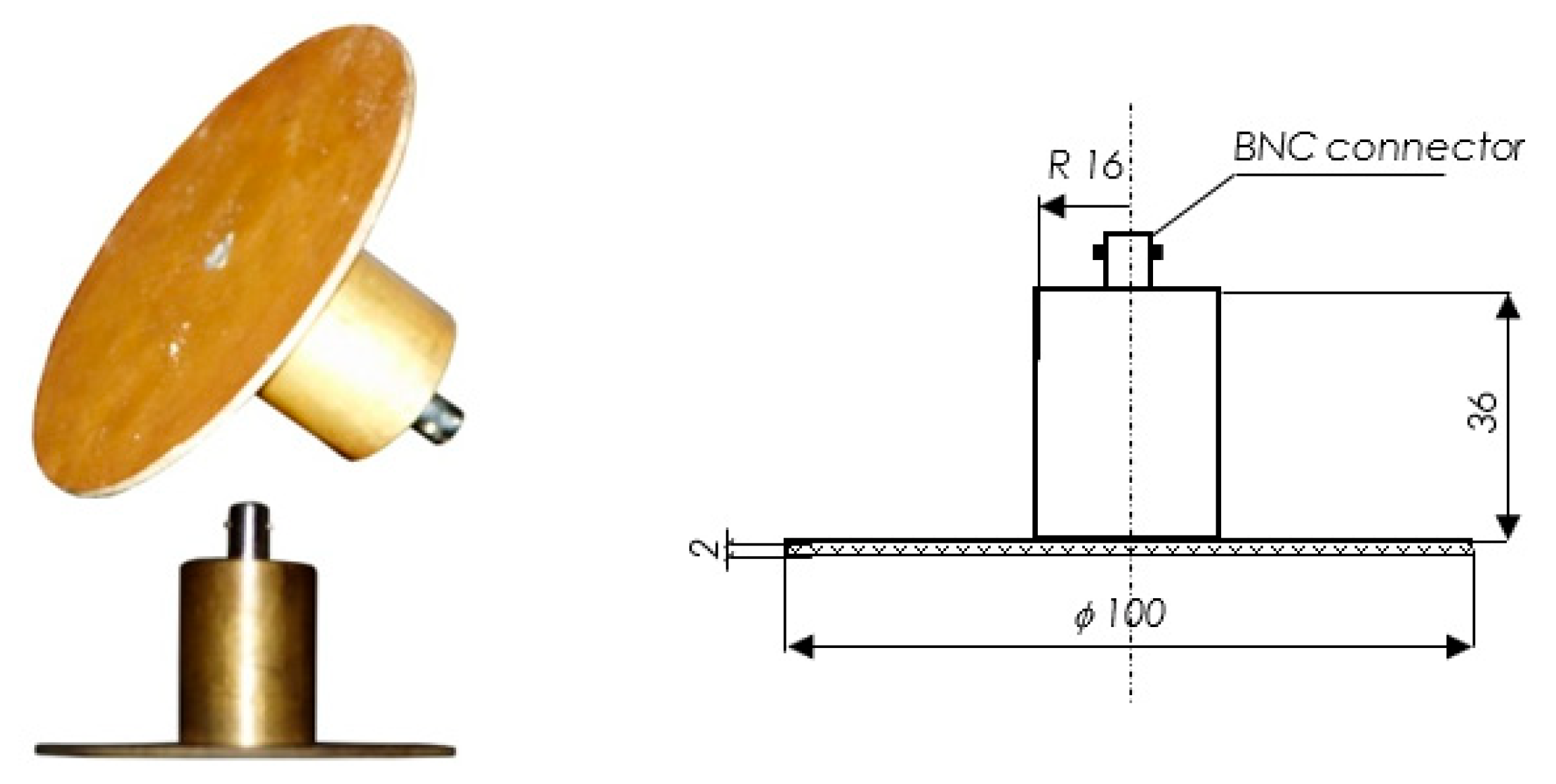
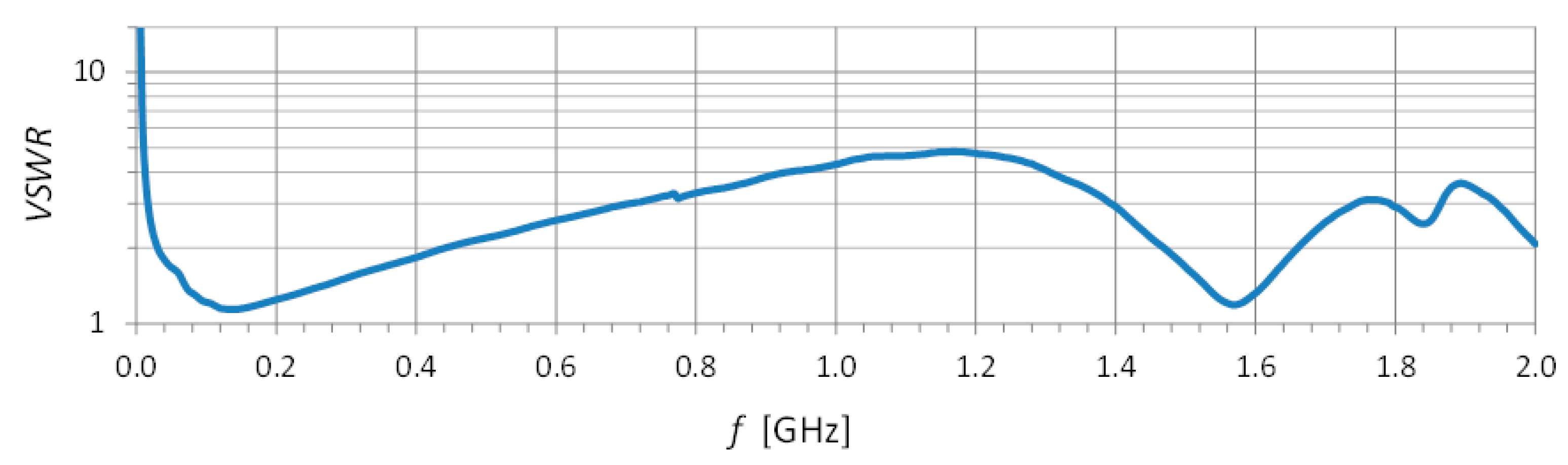
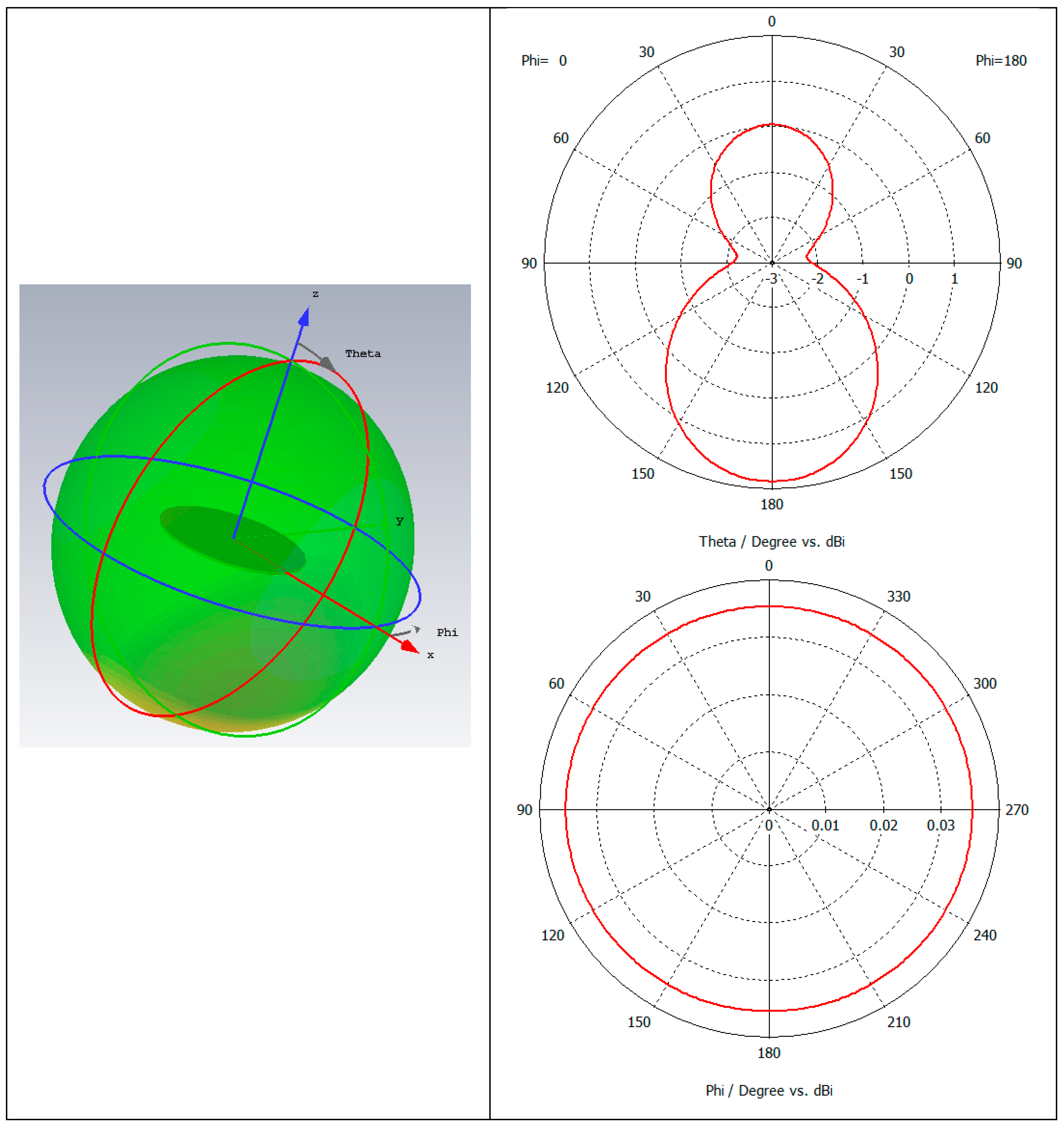
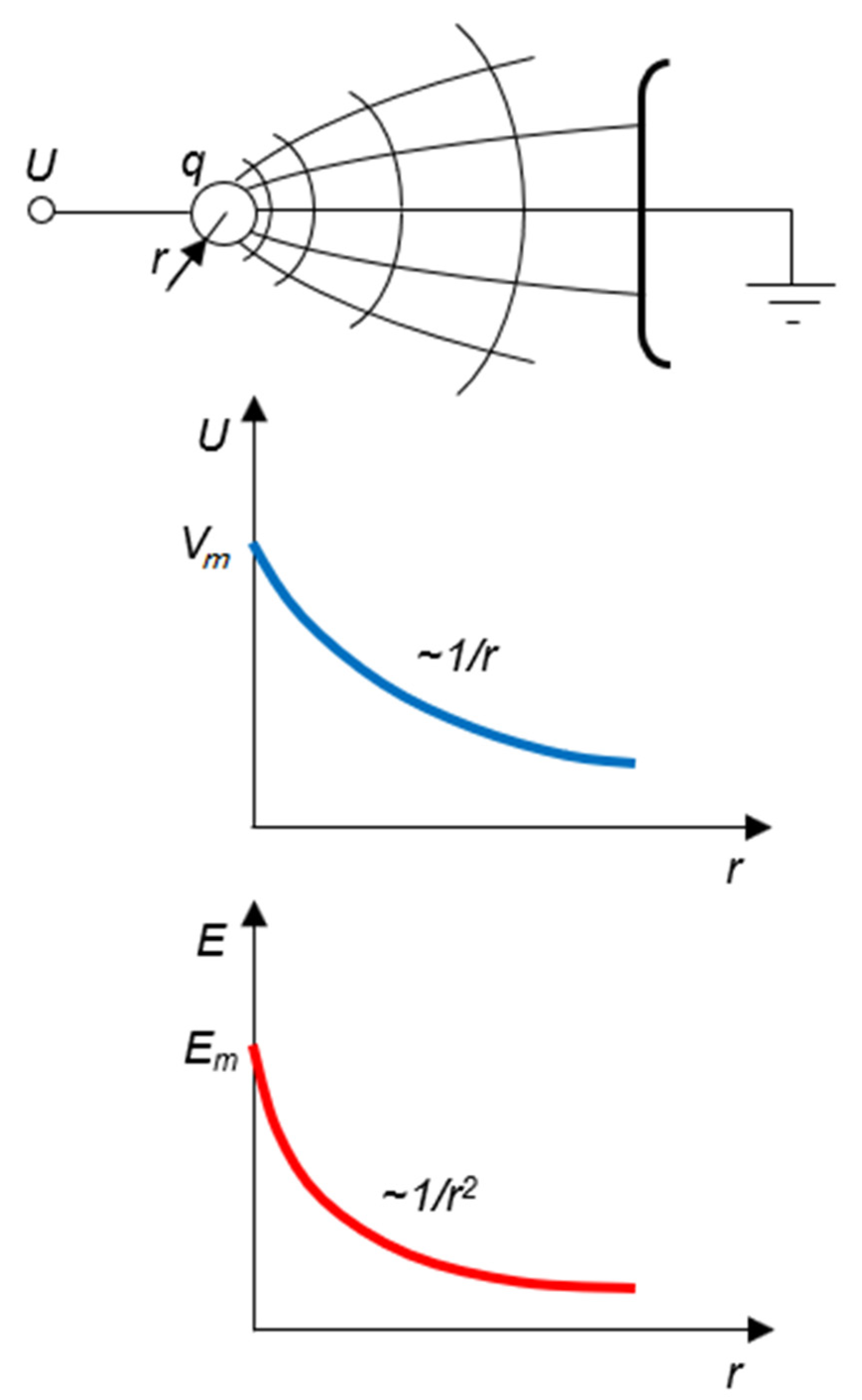
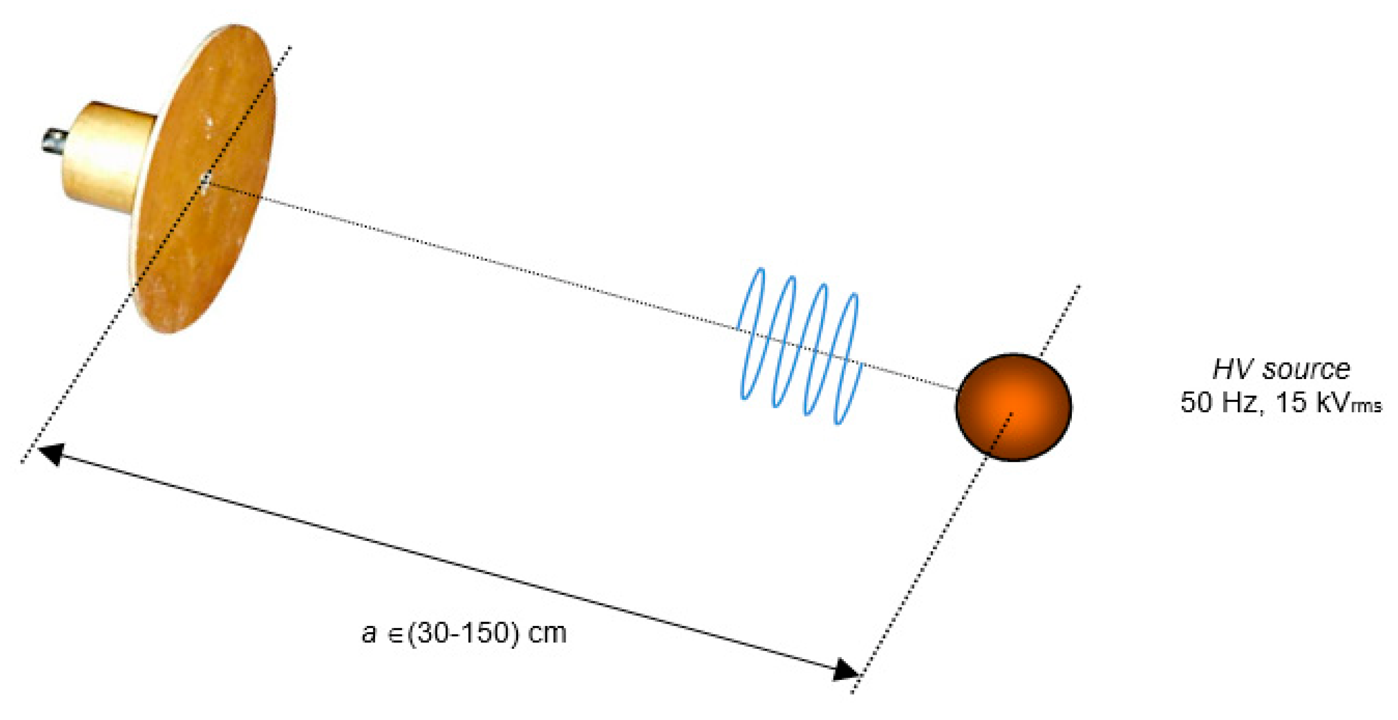
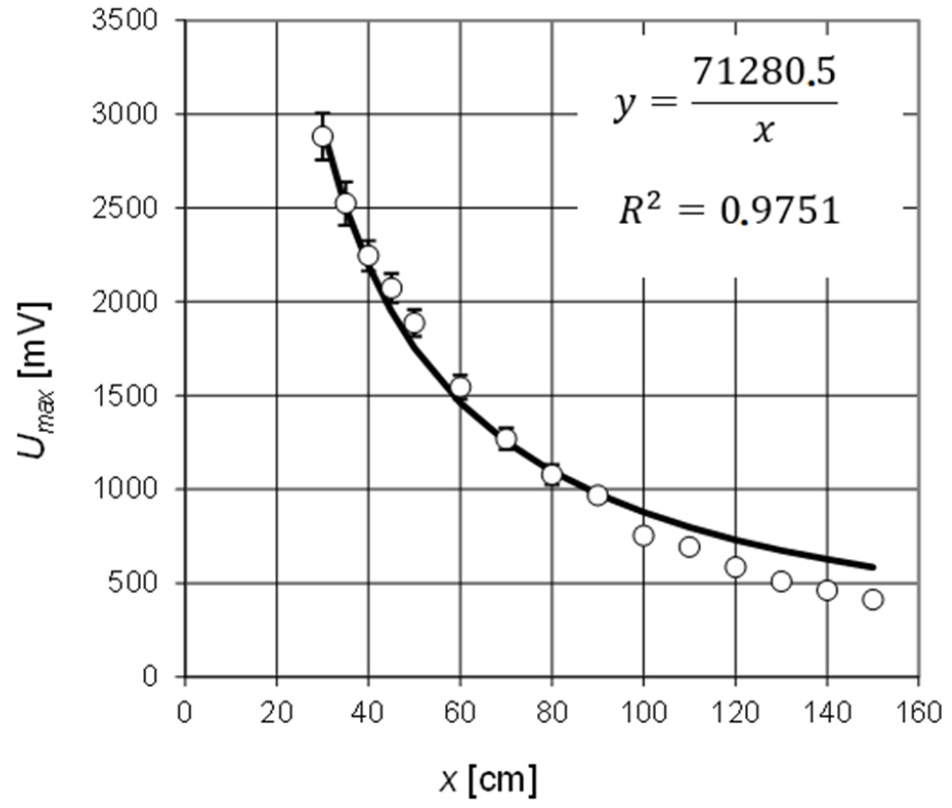
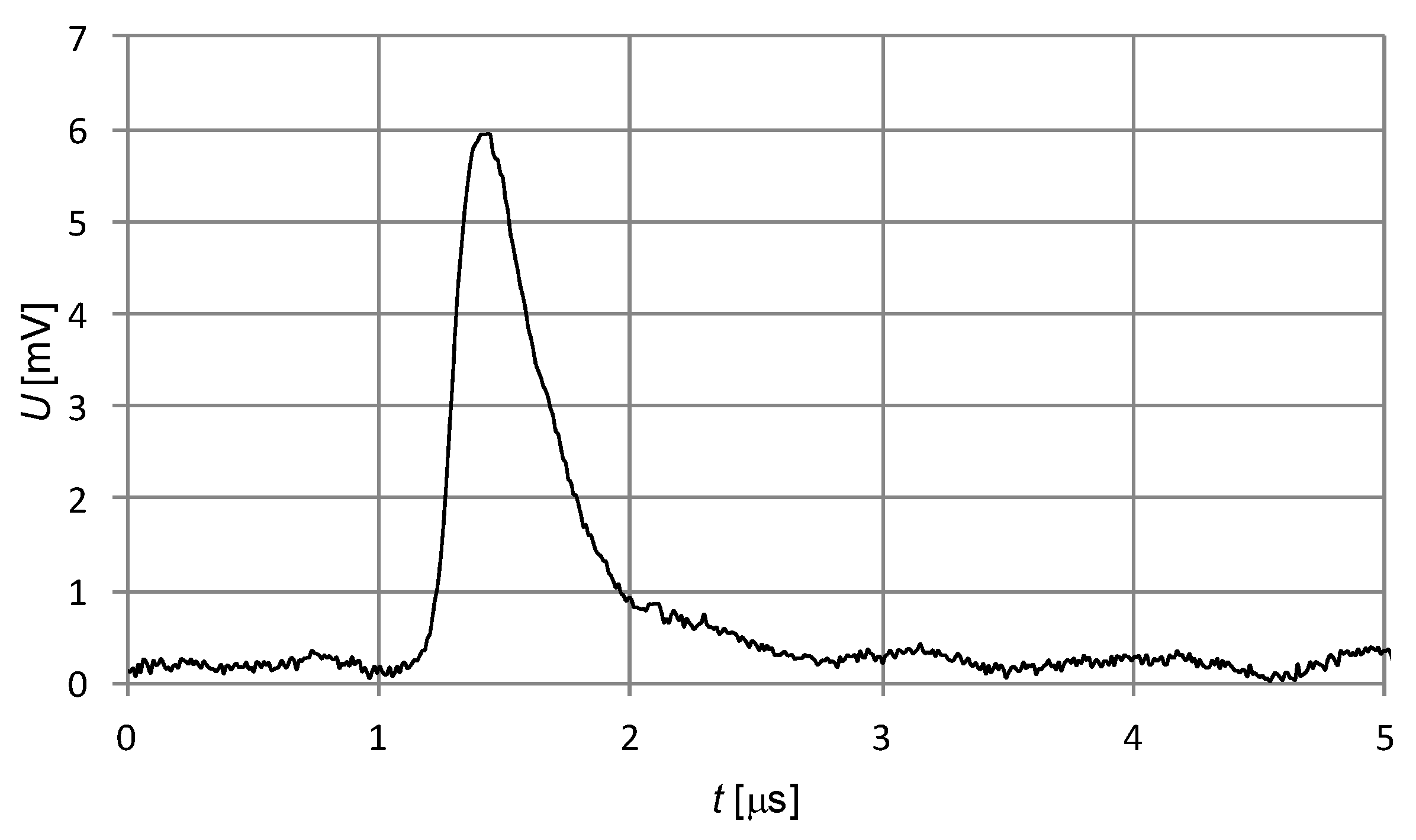
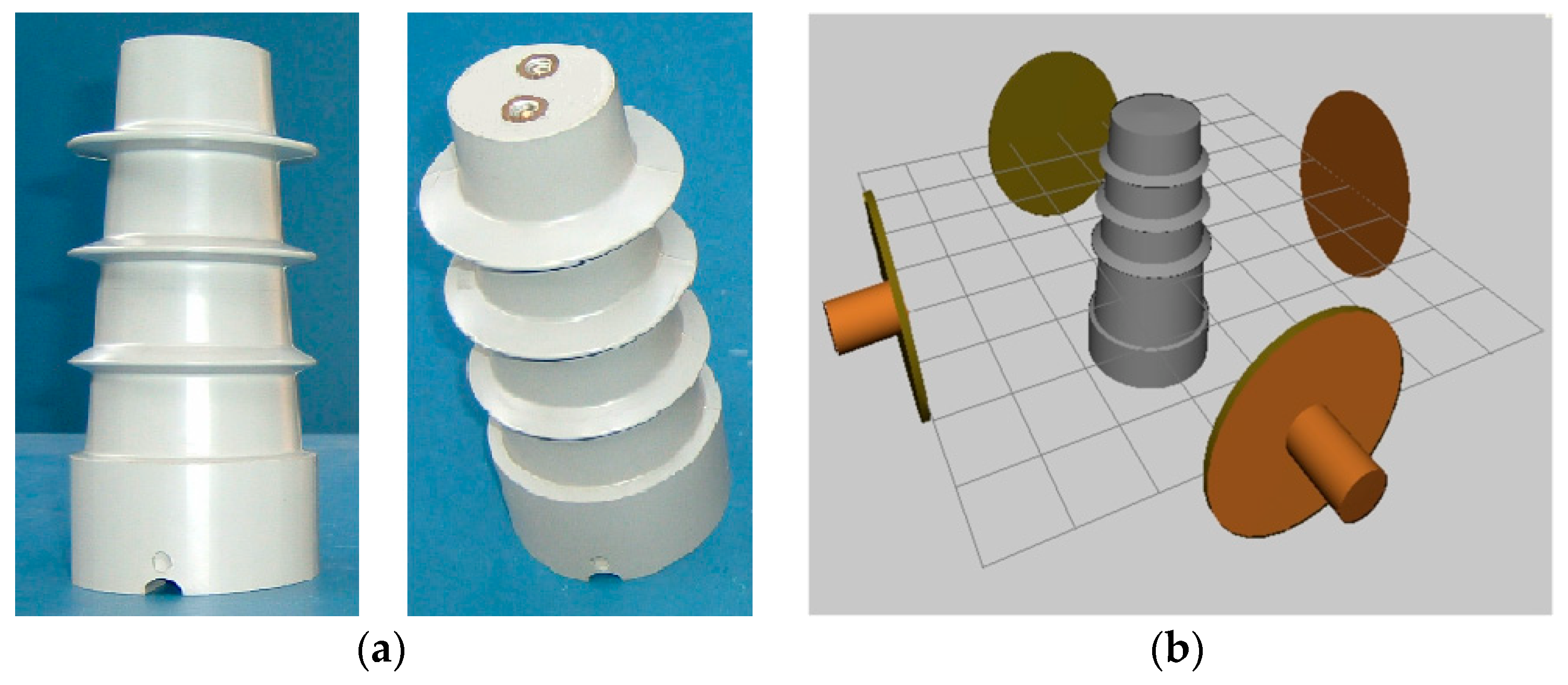
2. Materials and Methods

The requirements for sensors intended for the applications that are the subject of the research presented in this article are met by many different types of construction. The most common capacitive probes include unipoles, discs, spherical and hemispherical probes, conical, spiral and spiral-conical probes [18,19,20,21,22,23,24,25]. In the literature, you can also find newer solutions in this area, based on, for example, Hilbert-type antennas [26], loop [27], microstrip [28] or “bowtie” [29], which enable signal detection in a very selectively defined frequency band.
A disc probe with a structure as shown in Figure 1 has been chosen for the tests. This type of sensor is characterized by the appropriate frequency response required for partial discharge tests in high-voltage facilities. The construction of the sensor is as follows: This is a laminate, made of a layer of dielectric material coated on both sides with a layer of copper. A glass fabric impregnated with epoxy resin was used as the dielectric, while the metal layers were applied by sputtering. While maintaining the appropriate diameter of at least a few centimeters, the probe has sufficient sensitivity, which, however, depends on the direction of signal propagation relative to its location.
One of the important properties that should be determined for a capacitive probe is the frequency response, i.e., the dependence of the amplitude of the signal recorded by the probe on the frequency of the signal emitted by the source. Such defined bandwidth can be determined in various ways. In the high-frequency range of the signal, the sensor is treated as an antenna, therefore the band is determined using special indicators generally accepted in radio telecommunications. One of them is the input impedance of the probe. Due to the connections made with coaxial cables, the connectors, the input impedance of the amplifiers and the used measuring equipment, the input impedance of the antenna should be equal or close to 50 Ω, which is a commonly accepted standard. The degree of impedance matching is determined by the standing wave ratio (VSWR) or return loss (RL). The parameters are defined as follows:
R L = 10 log P i P r = 20 log Γ ,
V S W R = 1 + Γ 1 Γ ,
where:
  • Γ—voltage reflection coefficient;
  • Pi—input power;
  • Pr—power reflected from the input.
The parameters listed above are determined automatically using a specialized device—an antenna analyzer.
An antenna and spectrum analyzer KC901S+ by Measall Technology was used to determine the frequency response in the high and ultra-high frequency range. The measurements were each time preceded by a standard calibration procedure. As a result, the characteristics in Figure 2 were obtained.
For transmitting–receiving antennas in semi-professional systems, it is assumed that the VSWR value should not be higher than 2 (RL = 9.5 dB), which means that 11.1% of the power will be reflected from the antenna input (the signal will decrease by 0.5 dB). In practice, for receiving antennas used to monitor the electromagnetic spectrum, the acceptable value is VSWR = 3 (RL = 6 dB), i.e., it is allowed that 25% of the power will be reflected from the input, and the signal attenuation will be equal to 1.25 dB. It can be assumed that signal attenuation of 3 dB is acceptable in the case of PD detection, especially if an amplifier is used to increase the power level of the received signals.
Referring the results of the obtained characteristics to the above criteria, the disc probe has two useful bands: in the frequency range in the HF band (from 30 to 400 MHz) and in the narrow range of the UHF band (from 1.4 to 1.7 GHz), which is a range sufficient for the expected signal during measurements.
One of the important features of capacitive probes is directionality, which is defined as a measure of the ability to concentrate energy in one, distinguished direction at the expense of other directions [30]. This parameter is defined using the following formula:
D = U m U a v e ,
where:
  • Um—the maximum radiation density of a given antenna;
  • Uave—average radiation density.
Whether a probe is highly directional or not depends on its design. Knowing the directional pattern is important in several cases. Strong directionality means that the probe has a very narrow signal detection area, which is a great difficulty when it is mounted in a large facility whose operation is to be monitored. On the other hand, strong directionality makes it possible to limit the influence of disturbances from neighboring sources or objects when detecting a signal from a specific, small area, what can be very useful, for example, in high voltage measurements [31]. Poor directionality, on the other hand, is very desirable for partial discharge measurements in large objects (such as a power transformer) because a large volume can be monitored by several probes. Directionality, even a small one, is important in every case where the amplitude of the measured signal is important for the analyzed problem (e.g., for the method of locating defects in the insulation system presented in this article).
In the case of determining the directional characteristics of the capacitive probe, the selection of the measurement methodology will depend on the frequency range of the source signal, i.e., it will be related to the issue of the far and near field. In order to determine the directional characteristics for high and ultra-high frequency signals, i.e., far field, the measurement is quite complicated because it requires a much larger space between the source and the antenna, which should be free of artificial and natural obstacles causing wave reflections, which often requires the use of special materials that absorb electromagnetic waves. Such conditions can be artificially created in a closed room, but the creation of such a so-called anechoic chamber requires considerable financial outlays. For the above reasons, in practice, to determine the directionality, analytical methods are used for less complex structures or numerical methods when the antenna has a complex shape and complex characteristics are expected.
Therefore, the behavior of the antenna in the far field at a signal frequency of 1 GHz was numerically simulated in CST Studio Suite® package. The obtained result was presented on two- and three-dimensional charts (Figure 3), which reflect the energy gain of a given antenna calculated in relation to a theoretical isotropic antenna (hence expressed in dBi units). The Phi angle in the graphs corresponds to the rotation in the XY plane (horizontal plane relative to the orientation of the probe) and the Theta angle in the XZ plane (vertical plane relative to the orientation of the probe). The red curve corresponds to the energy gain projected onto a given plane.
Analyzing the obtained results, the probe exhibits strong anisotropy, which means that it is highly directional. Knowledge of the directional characteristics allows for the proper positioning of the probes depending on the application; therefore, it is of very practical importance. This knowledge was used in the research.
During measurements made by capacitive probes in the near field, it should be borne in mind that the distance between the signal source and the probe is of key importance for the value of the amplitude of the recorded signal. This results directly from the distribution of the electric field around the object located at the electrical potential [32]. Using the classic non-uniform field (sphere–plate system—Figure 4), this relationship can be described using the formula:
V r = P 1 E d r = P 1 q 4 π ε 0 r 2 d r = q 4 π ε 0 r ,
where:
  • q—the total electric charge of the ball;
  • P1—a point in space at a distance r from the center of the sphere [33].
The presented relationship is a significant simplification in relation to reality, but the general nature of the relationship is preserved, which will be confirmed using laboratory tests.
In order to verify the hypothesis about the influence of distance on the voltage registered by the probe, an appropriate experiment was carried out. Of course, one should be aware that due to the influence of various factors (related, for example, to the proximity of various devices and earthed elements), the obtained results will be primarily quantitative, but they are certainly important from the point of view of the described technique measurement.
The distance characteristic, i.e., the dependence of the amplitude of the signal registered by the sensor on the distance from the voltage source, was determined as follows: The capacitive probe was placed at distance a from a stable electromagnetic wave source, which was a sphere electrode with a diameter of 10 cm, powered by AC voltage with a frequency of 50 Hz. This is shown in Figure 5. In order to obtain the appropriate precision, the distance between a given probe and the source was measured using a laser rangefinder. The RMS value of the voltage generated during the test was 15 kV. Additionally, all unnecessary elements that could somehow change the field distribution in the space between the probe and the sphere electrode were removed from the measuring cell, and the objects themselves were placed on insulating stands at a distance of 1.5 m from the ground. As a result of the tests, the characteristics were obtained, as shown in Figure 6. In addition to the results, the graph shows the approximation curves, in accordance with the assumed function:
y = A x
where:
  • A—a function parameter.
The coefficient A of the non-linear function was determined using the Levenberg-Marquardt algorithm implemented in the specialized Origin software by OriginLab. The graphs show the formulas of the obtained functions and the value of the R2 coefficient, which is a measure of the degree of fit.
Analyzing the obtained characteristics, it can be seen that the used Function (5) correctly reflects the nature of the dependence between the amplitude of the signal registered with the use of a capacitive sensor and the distance. This is confirmed by the high value of the R2 coefficient, which is at a level of 0.97. The determined relationship gives a base for proposing a new method of locating a fault in the insulation system, which will be presented in the next chapter.

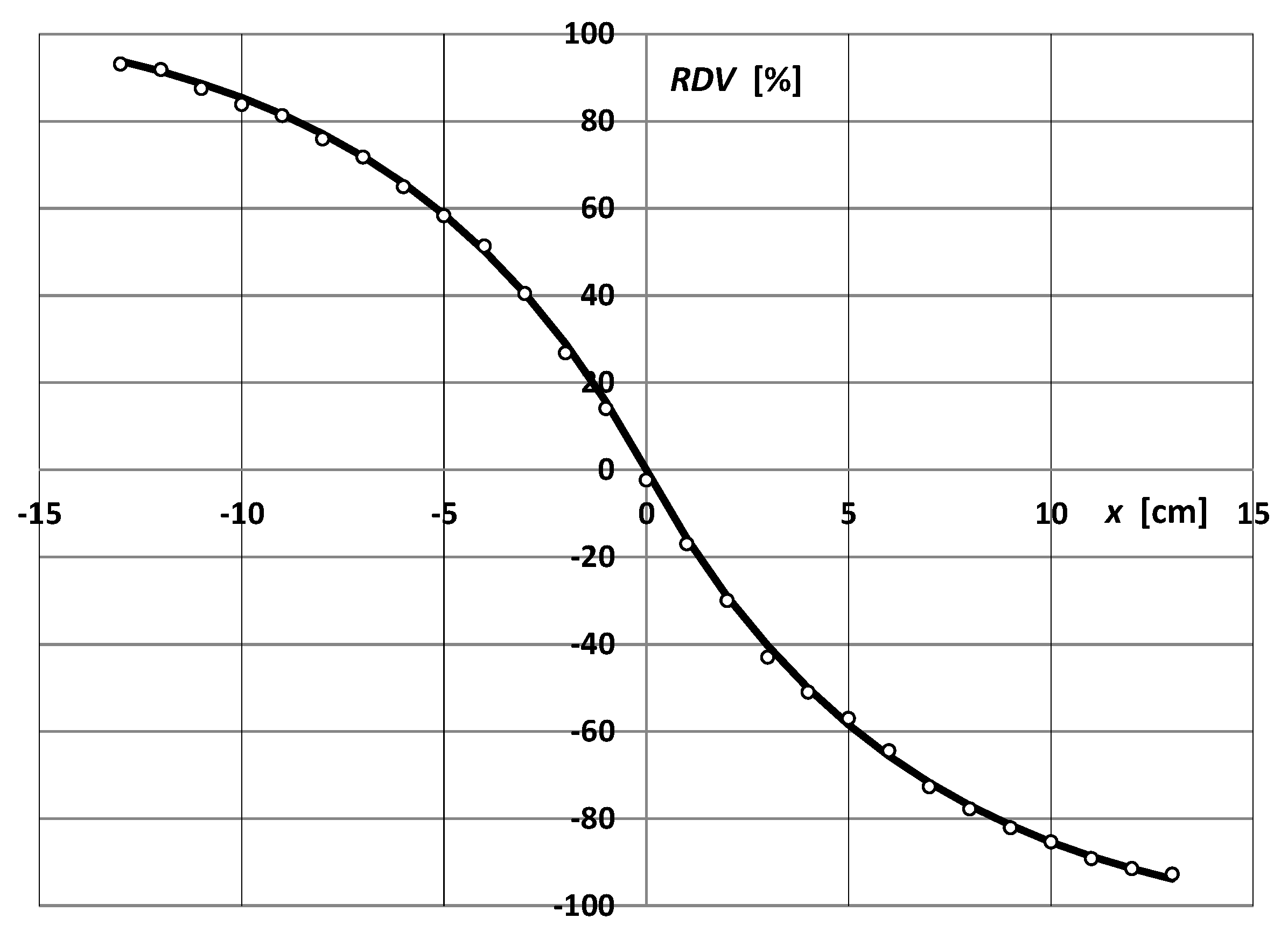
3. The Idea of the Localization Method Using a Pair of Capacitive Probes

The idea of the system for locating defects is based on the simultaneous registration of signals by two capacitive probes placed opposite each other (one-dimensional location). By analyzing the signals recorded by a pair of sensors, it can be shown that the relative difference in the values of the signals of both probes (RDV) (i.e., related to the higher value) depends on the position of the signal source in the axis of a given pair of probes. This relationship is in the form of an exponential function, the formula of which must be determined on the basis of laboratory measurements in the calibration process of a given pair of probes.
In order to calibrate the system, the probes are placed symmetrically in relation to the center of the system, at an equal height and at a distance that will allow for the subsequent placement of the test object in such a limited space. The source of the calibration signal should generate repetitive PD pulses. For this purpose, a built-in gas spark gap with reduced pressure was used, which at the voltage of 2 kV RMS generated PD pulses, as shown in Figure 7. The probes constituting a pair were spaced 40 cm apart. By changing the position of the reference PD source, an image of the dependence of the RDV on the position of the signal source in space was obtained, i.e., the calibration curve of a given pair of probes (Figure 8).
The relationship presented in Figure 8 can be approximated using the following function:
R D V = s g n ( x ) A 1 e A b s x t ,
where:
  • RDV—the relative difference in the values of the signals recorded by the two probes;
  • x—the position of the PD source in the axis;
  • t, A—the constants.
Determining the value of RDV on the basis of measurements and transforming the function presented above to the form:
x = t l n 1 R D V s g n ( x ) · A ,
it is possible to determine the location of the PD source in the axis of the pair of probes, i.e., in one dimension.
Unfortunately, the above relationship allows for the precise location of the defect only when it is located no more than 5 cm from the axis between the probes or at the same distance from both probes. This is because with the change in the position of the source relative to the axis, the peak value of the recorded signal changes in a non-linear way; therefore, the relationship between the indications of the pair of probes shown in Figure 8 and described in Formulas (6) and (7) also changes. Of course, these changes also have a specific character, which can be described by a functional dependence. The parameter that would allow the introduction of an appropriate correction is information about the distance of the signal source from the axis of the probes. Such information can be obtained by having a second pair of probes, the axis of which is perpendicular to the axis of the first pair, i.e., as in the system configured for the two-dimensional location. In this situation, the indication of a particular pair of probes is used to determine the x or y coordinate, respectively, and to introduce a correction to the indication of the second pair of probes according to the dependence:
x = x p · k = x p · 1.1 + 0.0006 · y p 2 · 1.6 x p · x p 0.18 ,
y = y p · k = y p · 1.1 + 0.0006 · x p 2 · 1.6 y p · y p 0.18 ,
where:
  • x, y—the position of PD source after correction;
  • xp, yp—the coordinates determined on the basis of the Formula (7);
  • k—the correction factor.
Quite a complex formula for the correction factor k is the result of the analysis of the dependence of the value of the RDV parameter on the location of the defect in the entire area under consideration, and the coefficients contained in the formula were selected experimentally.
Figure 9 shows the effect of the standard location algorithm (a), taking into account the correction according to the algorithm described above (b). The test consisted in moving the source of PD pulses to different places in the area (10 in total) limited in the figure by a circle with a diameter of 17 cm to check how correctly the given algorithm indicates the place of signal propagation. Of particular importance were those locations that deviated from the axis of a given pair of sensors. As can be seen from the figure, the use of the correction factor k makes it possible to determine the location of the PD source with much greater accuracy (up to 0.5 cm) in the entire covered area.
The tests presented above concerned determining the position of the reference source of the PD signal, which was the spark gap. In the next part of this article, a test of the method for locating a defect existing in a real object will be presented.

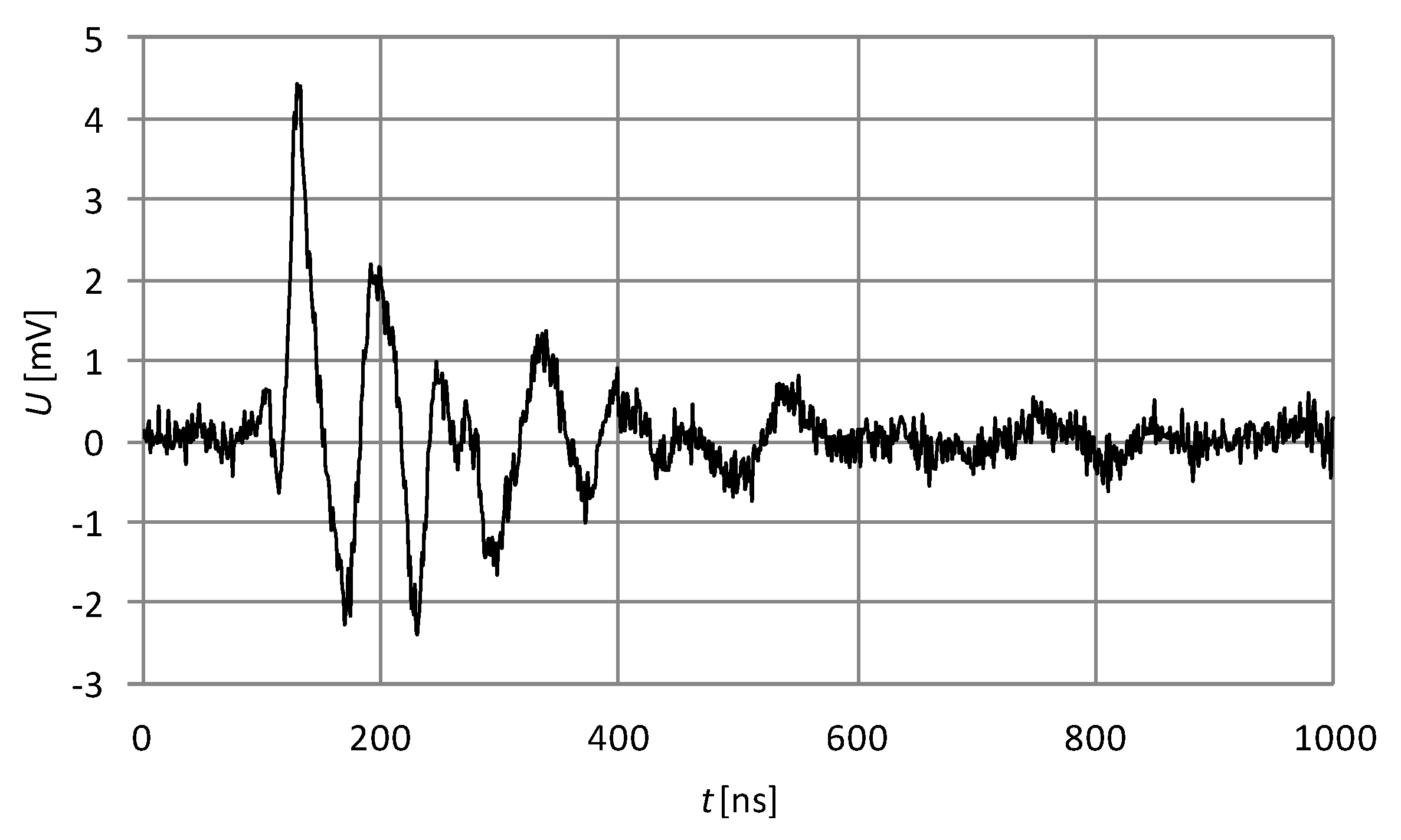
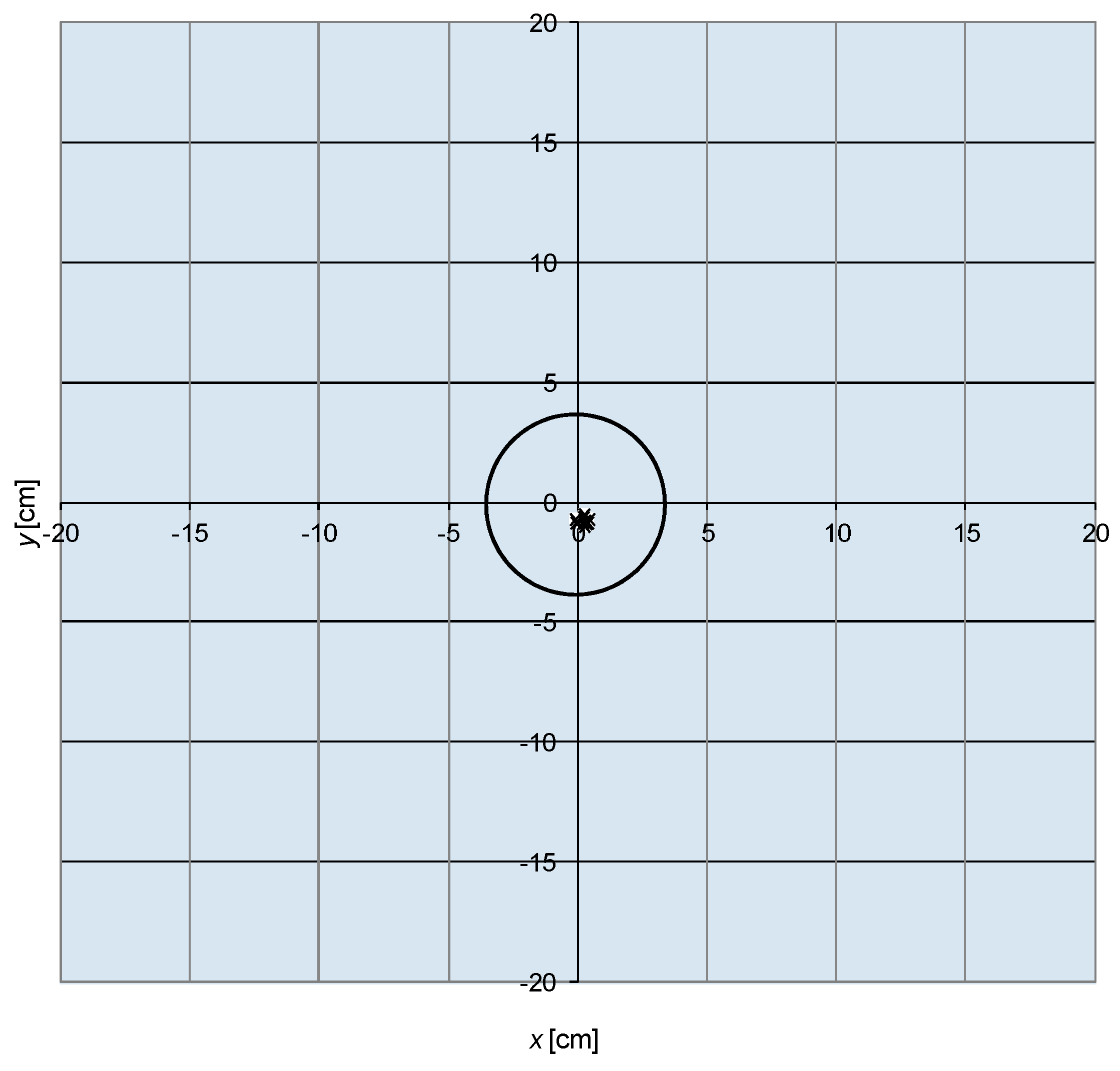
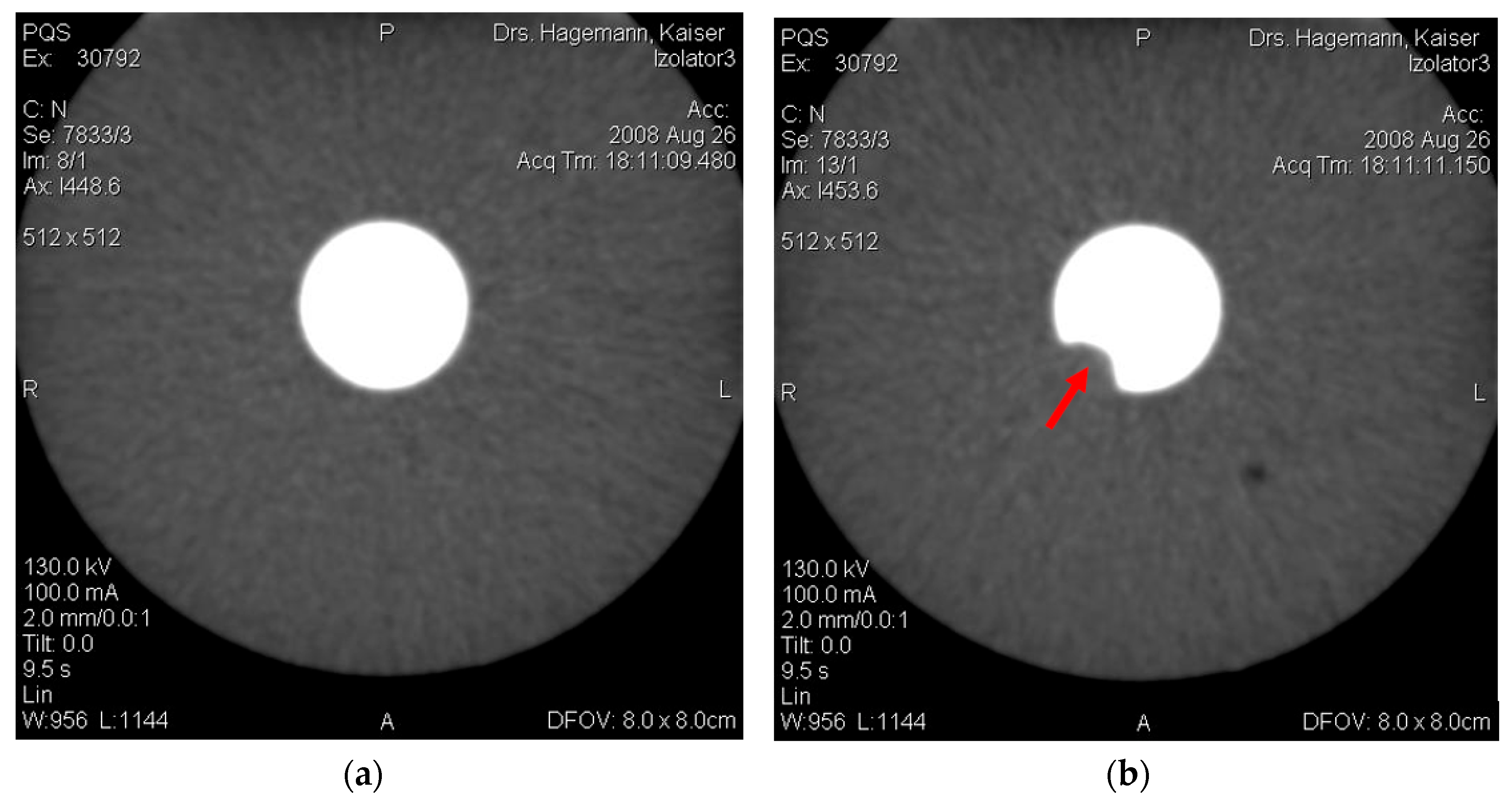
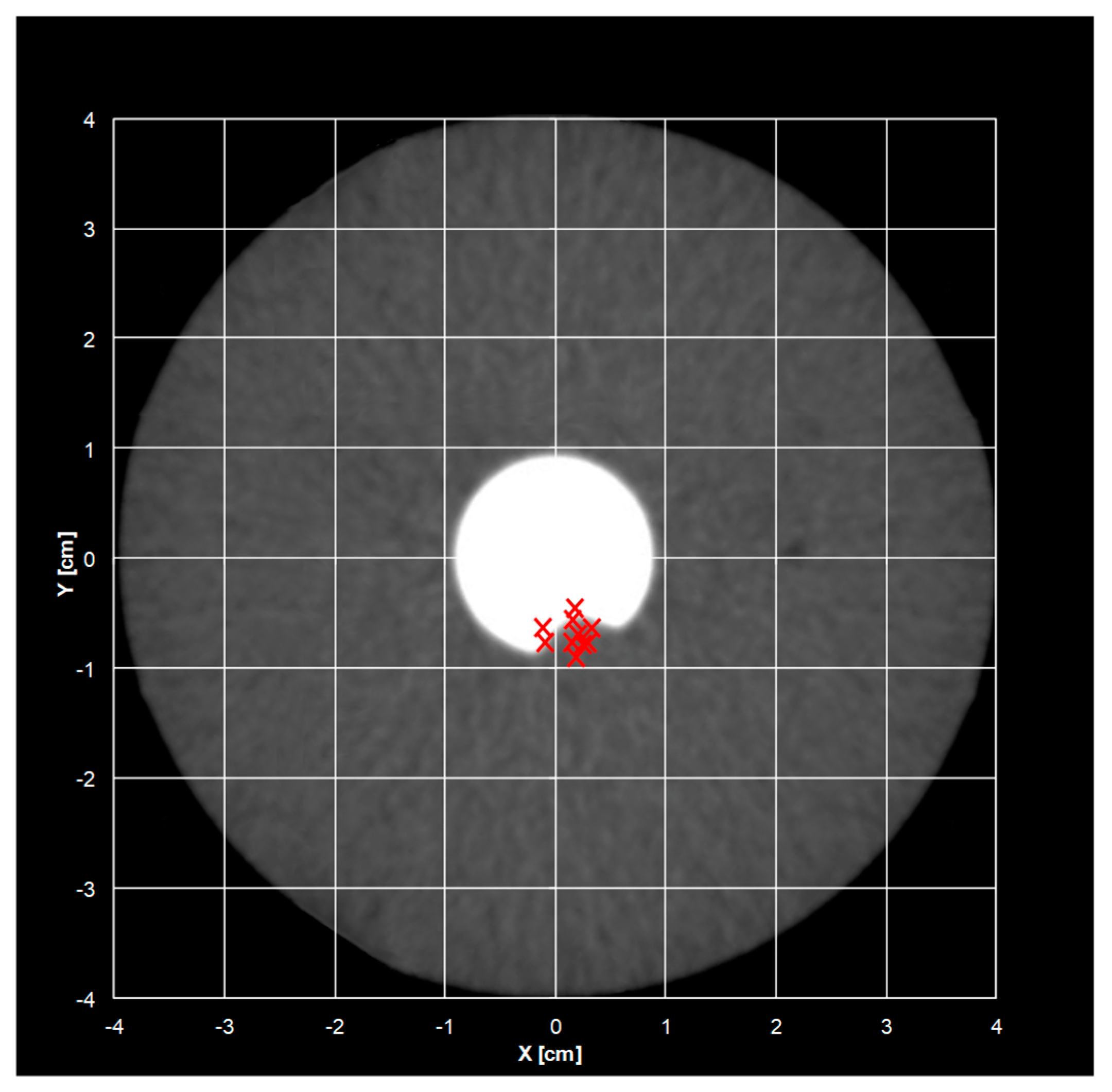
4. Results and Discussion

The tested object was an indoor support insulator with an internal resistive–capacitive divider working as a voltage indicator (Figure 10). The object was selected for testing on the basis of previous measurements using the IEC 60270 method, which allowed the presence of repetitive and stable PD pulses to be detected. In addition, this object could be X-rayed to indicate the actual location of the defect in its structure.
After preparing two pairs of capacitive sensors, the tested insulator was placed in the center of the probe system, and several measurement series were performed at a voltage of 10 kV RMS. As a result of the measurements, repeatable waveforms of the PD pulses generated by the insulator defect were obtained. All sensors recorded pulses of a similar shape, as shown in Figure 11. The magnitude of the registered signal was 4–20 mV. The PD-generating defect was an air gap resulting from improper filling of the space around the core by the epoxy resin.
During the measurements, PD pulses were generated and recorded simultaneously by both pairs of sensors. A series of ten measurements was collected. The localization was carried out according to the algorithm presented earlier. The analysis indicated an area of about 0.25 cm2 (0.5 × 0.5 cm) where the PD source was probably located (Figure 12).
In order to verify the results obtained with the use of capacitive probes, tests were carried out based on X-ray flaw detection [34]. As a result of this analysis, the obtained images indicated the existence of a defect in the core of the insulator. The use of X-ray tomography made it possible to locate the defect in the middle of the height of the insulator. Figure 13 shows the X-ray image of the part of the core without a defect and the image of the core with a defect. This type of defect can be a source of partial discharges.
After appropriate processing of the image and superimposing the results obtained from the location with the use of capacitive probes, a very good agreement was obtained, which is shown in Figure 14. The core defect visible in the X-ray image coincides with the x symbols denoting a defect located with the use of the method of an associated pair of sensors.

5. Conclusions

In this article, the idea of the location of defects of insulation based on the analysis of the signal of PD pulses registered by a system of capacitive sensors was presented.
It was shown that on the basis of the assessment of the relative difference of values (RDV) of the signal recorded by two sensors, it is possible to determine the position of a PD pulse source in a one-dimensional space. Using a second pair of probes allows for location in a 2D space. More further works will also be oriented toward creating the arrangement for location in a 3D space.
On account of the exponential character of dependence of the amplitude of the signal recorded by the probe on the distance from its source, the method is limited to insulation systems of a size that can be located in a square about 40 × 40 cm in dimensions. Probably applying appropriate amplifiers will allow for widening the area of the method.
Next works should take into consideration further verification of the method, the assessment of showing inaccuracy, the influence of multisource defects to the explicitness of the location and the influence of various types of insulation designs (with complex structures) on the correctness of the location.

Funding

This research was financed by the Poznan University of Technology’s financial resources for statutory activity. Number of the project: 0711/SBAD/4560.

Institutional Review Board Statement

Not applicable.

Informed Consent Statement

Not applicable.

Data Availability Statement

Not applicable.

Conflicts of Interest

The authors declare no conflict of interest.

References

  1. Nadolny, Z. Electric Field Distribution and Dielectric Losses in XLPE Insulation and Semiconductor Screens of High-Voltage Cables. Energies 2022, 15, 4692. [Google Scholar] [CrossRef]
  2. Sikorski, W.; Walczak, K.; Szymczak, C.; Gil, W. On-Line Partial Discharge Monitoring System for Power Transformers Based on the Simultaneous Detection of High Frequency, Ultra-High Frequency, and Acoustic Emission Signals. Energies 2020, 13, 3271. [Google Scholar] [CrossRef]
  3. Luo, Y.; Li, Z.; Wang, H. A Review of Online Partial Discharge Measurement of Large Generators. Energies 2017, 10, 1694. [Google Scholar] [CrossRef] [Green Version]
  4. Wotzka, D.; Sikorski, W.; Szymczak, C. Investigating the Capability of PD-Type Recognition Based on UHF Signals Recorded with Different Antennas Using Supervised Machine Learning. Energies 2022, 15, 3167. [Google Scholar] [CrossRef]
  5. Florkowski, M. Classification of Partial Discharge Images Using Deep Convolutional Neural Networks. Energies 2020, 13, 5496. [Google Scholar] [CrossRef]
  6. Kumar, H.; Shafiq, M.; Hussain, G.A.; Kumpulainen, L.; Kauhaniemi, K. Classification of PD Faults Using Features Extraction and K-Means Clustering Techniques. In Proceedings of the 2020 IEEE PES Innovative Smart Grid Technologies Europe (ISGT-Europe), The Hague, The Netherlands, 26–28 October 2020; pp. 919–923. [Google Scholar]
  7. Cai, J.; Zhou, L.; Zhang, Y.; Wang, D.; Liao, W.; Zhang, C. Convenient Online Approach to Multisource Partial Discharge Localization in Transformer. IEEE Trans. Ind. Electron. 2022, 69, 9440–9450. [Google Scholar] [CrossRef]
  8. Sikorski, W. Development of Acoustic Emission Sensor Optimized for Partial Discharge Monitoring in Power Transformers. Sensors 2019, 19, 1865. [Google Scholar] [CrossRef] [PubMed] [Green Version]
  9. Ilkhechi, H.D.; Samimi, M.H. Applications of the Acoustic Method in Partial Discharge Measurement: A Review. IEEE Trans. Dielectr. Electr. Insul. 2021, 28, 42–51. [Google Scholar] [CrossRef]
  10. Besharatifard, H.; Hasanzadeh, S.; Heydarian-Forushani, E.; Alhelou, H.H.; Siano, P. Detection and Analysis of Partial Discharges in Oil-Immersed Power Transformers Using Low-Cost Acoustic Sensors. Appl. Sci. 2022, 12, 3010. [Google Scholar] [CrossRef]
  11. Chai, H.; Phung, B.T.; Mitchell, S. Application of UHF Sensors in Power System Equipment for Partial Discharge Detection: A Review. Sensors 2019, 19, 1029. [Google Scholar] [CrossRef] [Green Version]
  12. Karami, H.; Askari, F.; Rachidi, F.; Rubinstein, M.; Sikorski, W. An Inverse-Filter-Based Method to Locate Partial Discharge Sources in Power Transformers. Energies 2022, 15, 1988. [Google Scholar] [CrossRef]
  13. Lee, H.M.; Lee, G.S.; Kwon, G.-Y.; Bang, S.S.; Shin, Y.-J. Industrial Applications of Cable Diagnostics and Monitoring Cables via Time–Frequency Domain Reflectometry. IEEE Sens. J. 2021, 21, 1082–1091. [Google Scholar] [CrossRef]
  14. Ariannik, M.; Azirani, M.A.; Werle, P.; Azirani, A.A. UHF Measurement in Power Transformers: An Algorithm to Optimize Accuracy of Arrival Time Detection and PD Localization. IEEE Trans. Power Deliv. 2019, 34, 1530–1539. [Google Scholar] [CrossRef]
  15. Sikorski, W. Active Dielectric Window: A New Concept of Combined Acoustic Emission and Electromagnetic Partial Discharge Detector for Power Transformers. Energies 2019, 12, 115. [Google Scholar] [CrossRef] [Green Version]
  16. Si, W.; Fu, C.; Yuan, P. An Integrated Sensor With AE and UHF Methods for Partial Discharges Detection in Transformers Based on Oil Valve. IEEE Sens. Lett. 2019, 3, 1–3. [Google Scholar] [CrossRef]
  17. Schmidt, R.O. Multiple Emitter Location and Signal Parameter—Estimation. IEEE Trans. Antennas Propag. 1986, 34, 276–280. [Google Scholar] [CrossRef] [Green Version]
  18. Agoris, P.; Meijer, S.; Smit, J.J. Sensitivity Check of an Internal VHF/UHF Sensor for Trans-former Partial Discharge Measurements. In Proceedings of the POWERTECH’07, Lausanne, Switzerland, 1–5 July 2007; pp. 2065–2069. [Google Scholar]
  19. Cleary, G.P.; Judd, M.D. UHF and Current Pulse Measurements of Partial Discharge Activity in Mineral Oil. IEE Sci. Meas. Technol. 2006, 153, 47–54. [Google Scholar] [CrossRef]
  20. Coenen, S.; Tenbohlen, S.; Markalous, S.M.; Strehl, T. Attenuation of UHF Signals Regarding the Sensitivity Verification for UHF PD Measurements on Power Transformers. In Proceedings of the International Conference on Condition Monitoring and Diagnosis, Beijing, China, 21–24 April 2008. [Google Scholar]
  21. Judd, M.D. Transient Calibration of Electric Field Sensors. IEE Sci. Meas. Technol. 1999, 146, 113–116. [Google Scholar] [CrossRef] [Green Version]
  22. Li, J.H.; Si, W.R.; Yuan, P.; Li, Y.M.; Li, Y.M. Propagation Characteristic Study of Partial Discharge UHF Signal outside Transformer. In Proceedings of the International Conference on Condition Monitoring and Diagnosis, Beijing, China, 21–24 April 2008; pp. 1078–1080. [Google Scholar]
  23. Lopez-Roldan, J.; Tang, T.; Gaskin, M. Design and Testing of UHF Sensors for Partial Discharge Detection in Transformers. In Proceedings of the International Conference on Condition Monitoring and Diagnosis, Beijing, China, 21–24 April 2008; pp. 1052–1055. [Google Scholar]
  24. Ono, M.; Matsuyama, Y.; Otaka, N.; Yamagiwa, T.; Kato, T. Experience of GIS Condition Diagnosis Using Partial Discharge Monitoring by UHF Method. In Proceedings of the International Conference on Condition Monitoring and Diagnosis, Beijing, China, 21–24 April 2008; pp. 1108–1110. [Google Scholar]
  25. Wu, Q.; Liu, G.; Xia, Z.; Lu, L. The study of Archimedean spiral antenna for partial discharge measurement. In Proceedings of the Fourth International Conference on Intelligent Control and Information Processing (ICICIP), Beijing, China, 9–11 June 2013; pp. 694–698. [Google Scholar]
  26. Sikorski, W.; Szymczak, C.; Siodla, K.; Polak, F. Hilbert curve fractal antenna for detection and on-line monitoring of partial discharges in power transformers. Eksploat. I Niezawodn. 2018, 20, 343–351. [Google Scholar] [CrossRef]
  27. Hai-Feng, Y.; Yong, Q.; Yue, D.; Ge-Hao, S.; Xiu-Chen, J. Development of Multi-Band Ultra-High-Frequency Sensor for Partial Discharge Monitoring Based on the Meandering Technique. IET Sci. Meas. Technol. 2014, 8, 327–335. [Google Scholar] [CrossRef]
  28. Sarkar, B.; Mishra, D.K.; Koley, C.; Roy, N.K. Microstrip patch antenna based UHF sensor for detection of Partial Discharge in High Voltage electrical equipments. In Proceedings of the India Conference (INDICON), Pune, India, 11–13 December 2014; pp. 1–6. [Google Scholar]
  29. Suryandi, A.A.; Khayam, U. New Designed Bowtie Antenna with Middle Sliced Modification as UHF Sensor for Partial Discharge Measurement. In Proceedings of the International Conference on Smart Green Technology in Electrical and Information Systems (ICSGTEIS), Kuta, Indonesia, 5–7 November 2014; pp. 98–101. [Google Scholar]
  30. Slone, R. Practical Antenna Handbook; McGraw-Hill Education: New York, NY, USA, 2011. [Google Scholar]
  31. Walczak, K.; Sikorski, W. Non-Contact High Voltage Measurement in the Online Partial Discharge Monitoring System. Energies 2021, 14, 5777. [Google Scholar] [CrossRef]
  32. Nadolny, Z. Determination of Dielectric Losses in a Power Transformer. Energies 2022, 15, 993. [Google Scholar] [CrossRef]
  33. Nefyodov, E.I.; Smolsky, S.M. Electromagnetic Fields and Waves. Microwaves and mmWave Engineering with Generalized Macroscopic Electrodynamics; Springer: New York, NY, USA, 2019. [Google Scholar]
  34. Walczak, K.; Waszkiewicz, A. Detection of defects in the solid insulation of power devices using X-rays. Przegląd Elektrotechniczny 2010, 86, 279–282. [Google Scholar]
Figure 1. Capacitive disc sensor.
Energies 16 02297 g001
Figure 2. VSWR coefficient depending on the frequency of the signal.
Energies 16 02297 g002
Figure 3. Radiation characteristics in the vertical and horizontal planes (2D graphs) and in space (3D graph) for a disc antenna.
Energies 16 02297 g003
Figure 4. Distribution of potential and electric field intensity in a non-homogeneous sphere–plate system.
Energies 16 02297 g004
Figure 5. The method of determining the dependence of the amplitude of the signal registered by the sensor on the distance from the signal source.
Energies 16 02297 g005
Figure 6. Dependence of the signal registered by the sensor on the distance from the source for the disc probe; the points mean the measurement; the curve means the function approximating the relationship, described by the formula as in the diagram; R2—coefficient of determination for the selected function.
Energies 16 02297 g006
Figure 7. The pulse generated in the spark gap used to calibrate the system of two sensors.
Energies 16 02297 g007
Figure 8. The dependence of the relative difference of the values (RDV) of the signals registered by a pair of probes depending on the position of the gas spark gap on the x axis; using the points on the characteristics, the measured values were presented, while the continuous line was obtained from the calculations.
Energies 16 02297 g008
Figure 9. The figure shows the effect of individual location algorithms. The actual location of the signal source is marked with “x”, and the place indicated using the standard (a) or corrected (b) algorithm with “+”. The circle indicates the assumed maximum area available during the test (diameter 17 cm).
Energies 16 02297 g009
Figure 10. (a) General view of the test object and (b) location of two pairs of probes in relation to the object containing the defect.
Energies 16 02297 g010
Figure 11. PD pulse recorded during insulator test.
Energies 16 02297 g011
Figure 12. Location of the defect based on a series of ten measurements (the location of the defect is marked with x); the circle is the outline of the insulator placed centrally inside the system.
Energies 16 02297 g012
Figure 13. X-ray image of the insulator (selected cross-sectional planes): (a) part of the core without a defect and (b) core with a visible structure defect (marked with an arrow).
Energies 16 02297 g013
Figure 14. Cross-section of the insulator in the X-ray image with marked points of the defect located using the method of associated sensors.
Energies 16 02297 g014
Disclaimer/Publisher’s Note: The statements, opinions and data contained in all publications are solely those of the individual author(s) and contributor(s) and not of MDPI and/or the editor(s). MDPI and/or the editor(s) disclaim responsibility for any injury to people or property resulting from any ideas, methods, instructions or products referred to in the content.

