
Analysis of Discharge Failure Mechanism of IGBT Power Modules

Abstract
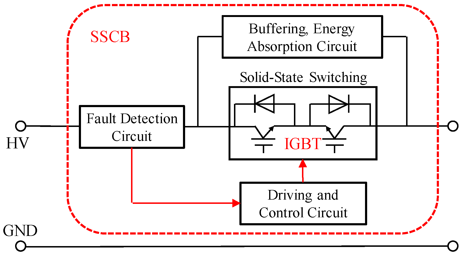
:1. Introduction
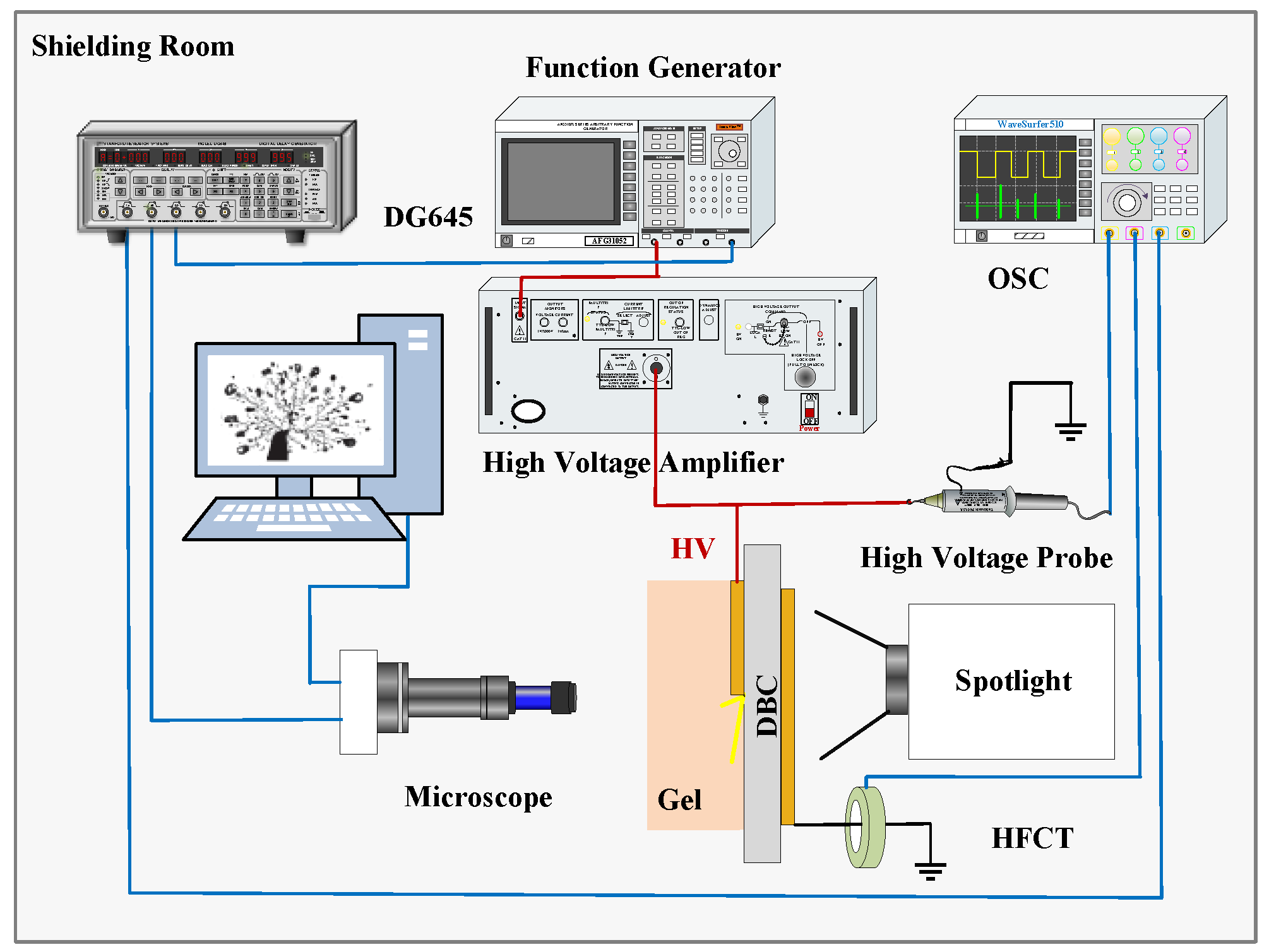
2. Experiment Platform
2.1. Partial Discharge Location
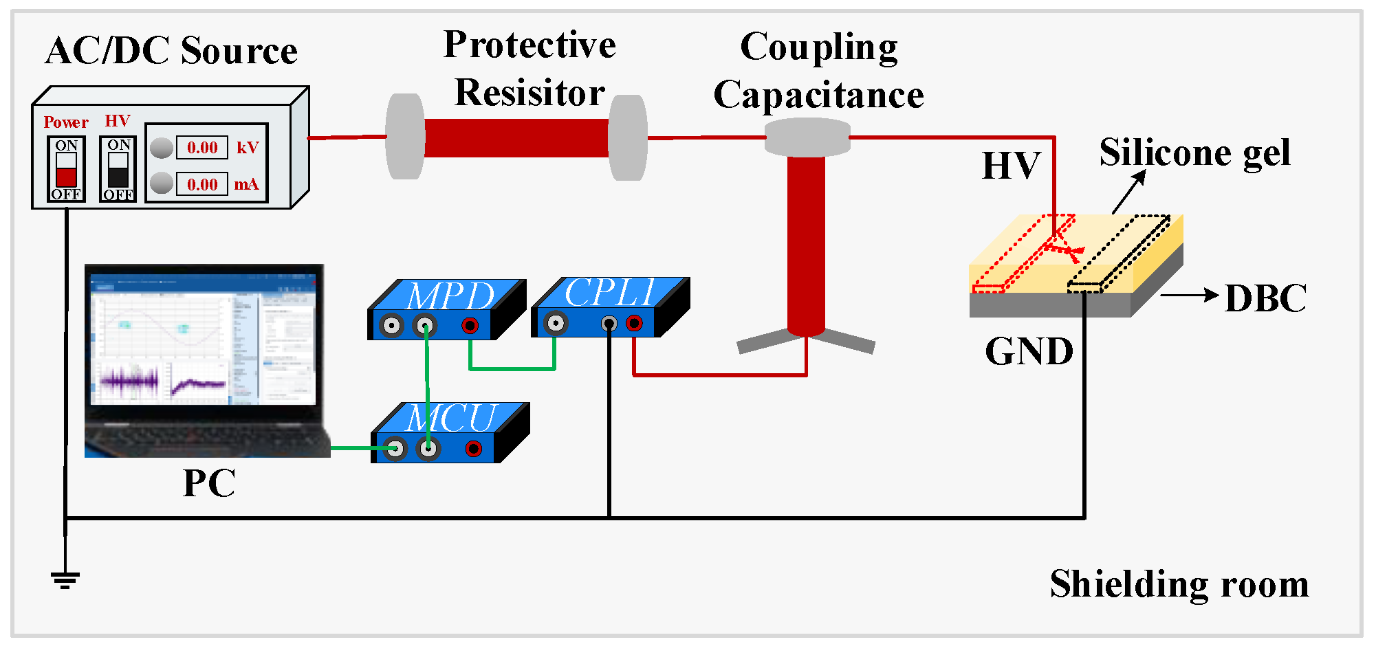
2.2. Partial Discharge Detection
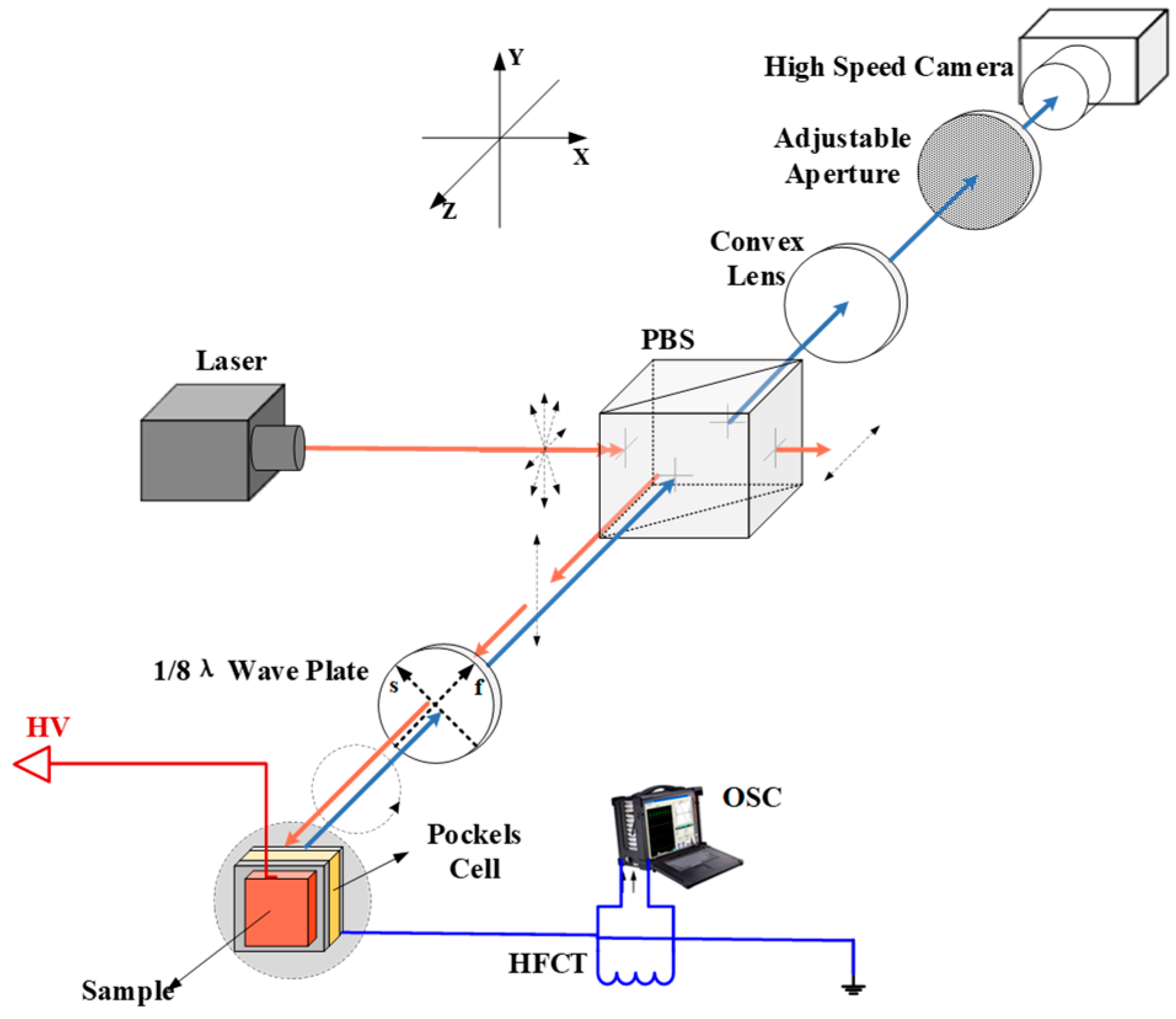
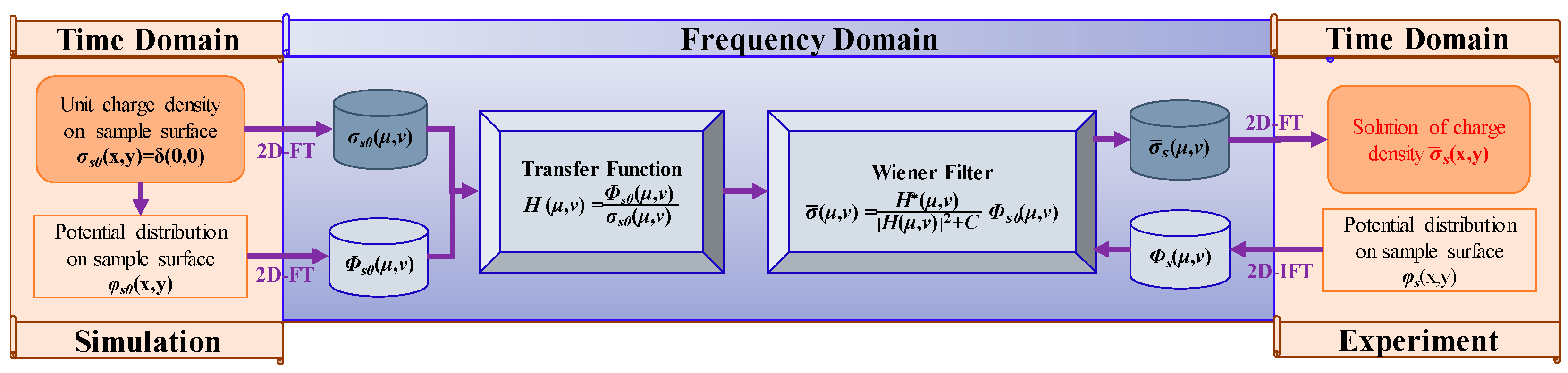
2.3. Interface Charge Measurement
- λ—wavelength of light in vacuum [m].
- n0—refractive index without electric field.
- l—length of the pockels crystal in the z-direction of electric field, [m].
- γ—electro-optic coefficient, [m/V−1].
- I—outgoing light intensity.
- I0—incident light intensity.
2.4. Electric Tree Observation
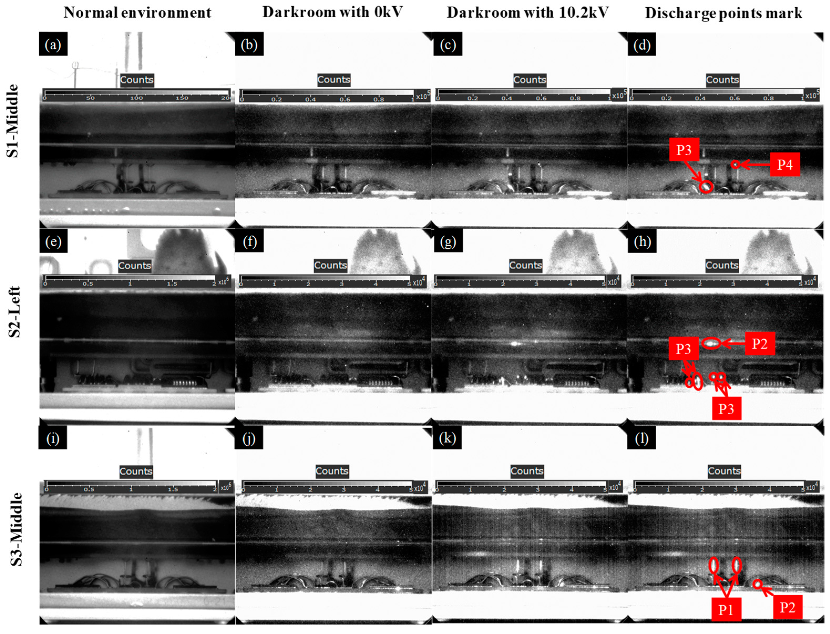
3. Initial Failure Location
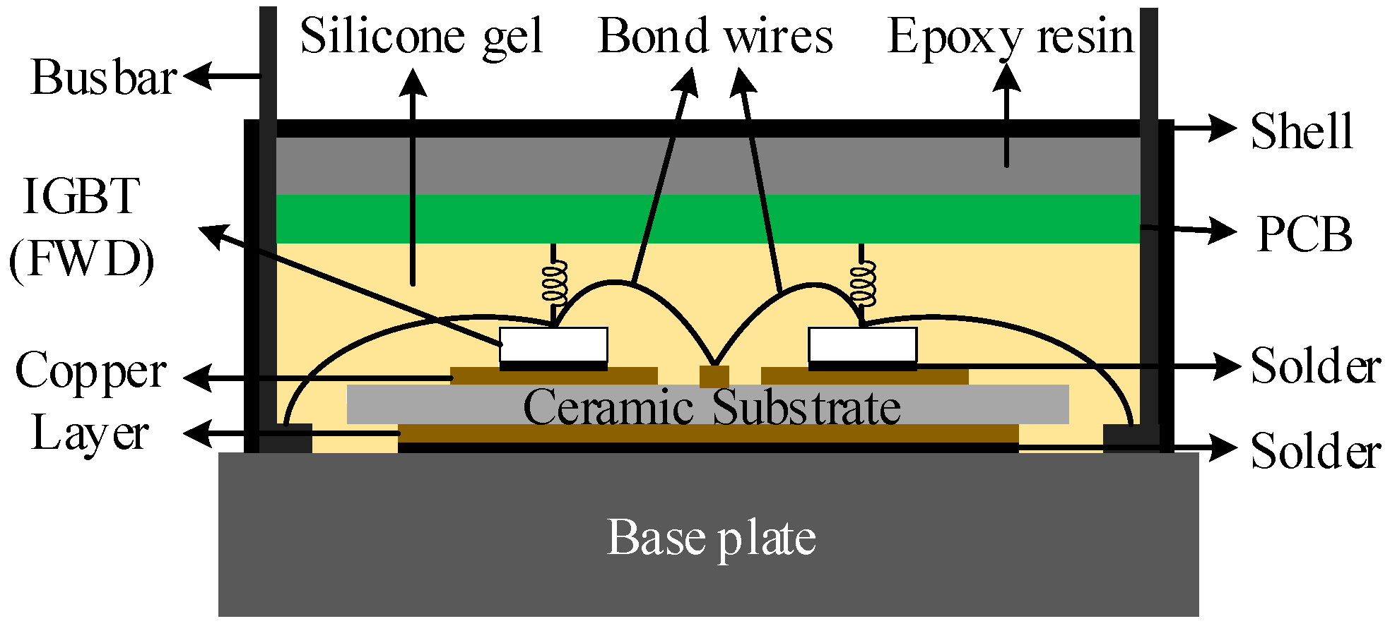
3.1. Sample Division
3.2. Discharge Location
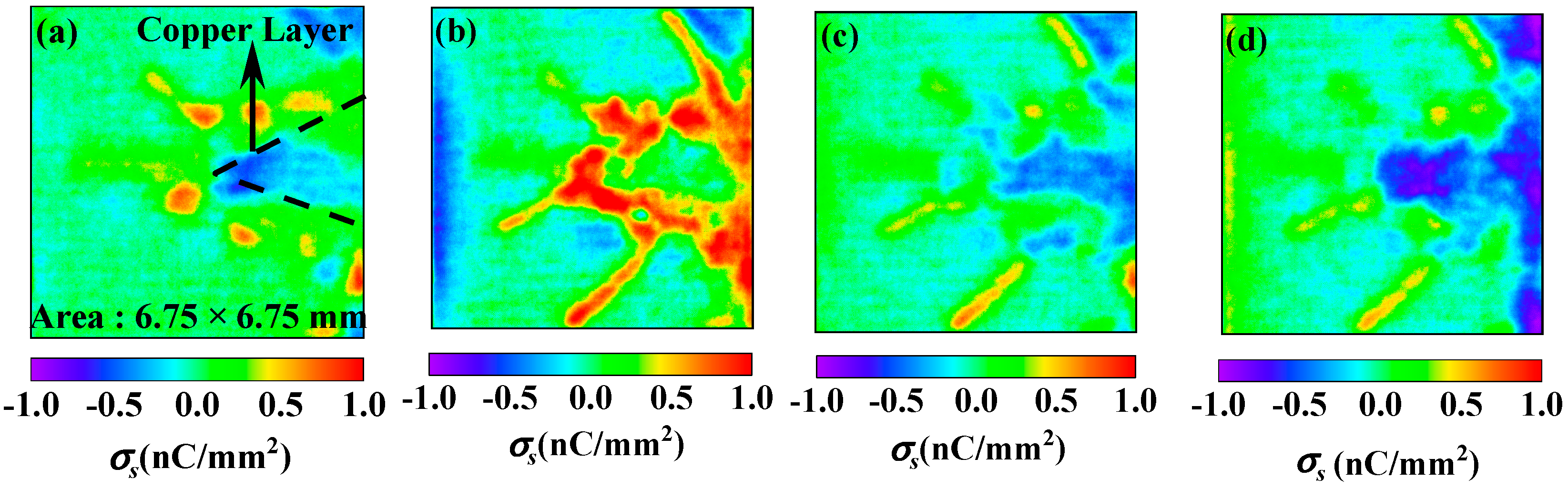
4. Interface Charge Kinetics
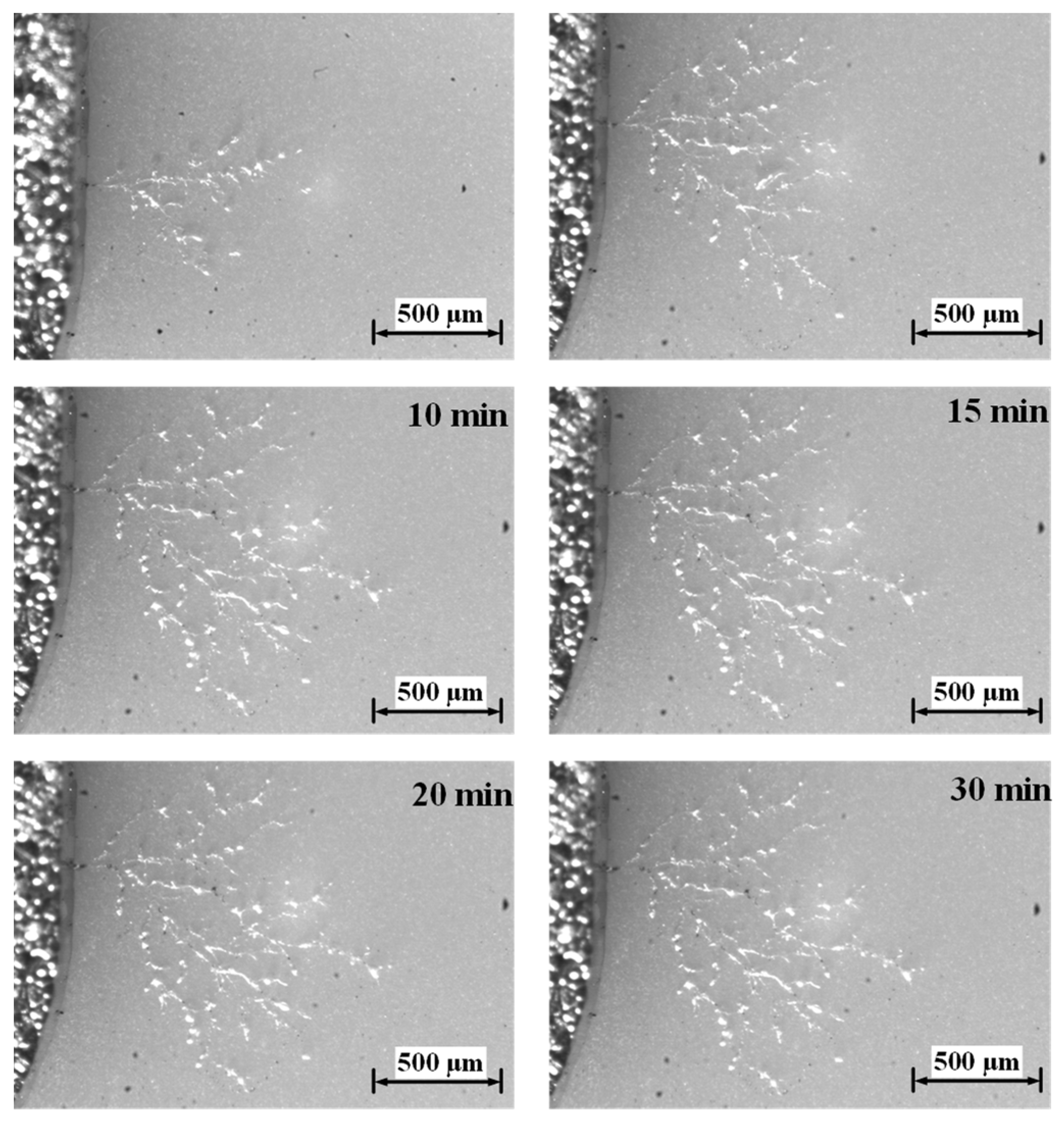
5. Electric Tree Extend
6. Conclusions
- (1)
- Interface discharge, gel discharge and solder joint discharge occur in the IGBT module. The interfacial discharge originating from the triple junction is the most dangerous failure. The discharge of bond wires and solder joints is reported here for the first time.
- (2)
- The kinetics of charge propagation from triple junctions along the ceramic–gel interface is shared. It reflects the spatial distribution of the discharge current.
- (3)
- The electric tree consists of filamentary channels and bubble-like cavities. The electric tree is lighter in color and is a transparent hollow channel.
Author Contributions
Funding
Data Availability Statement
Acknowledgments
Conflicts of Interest
References
- Allee, G.; Tschudi, W. Edison Redux: 380 Vdc brings reliability and efficiency to sustainable data centers. IEEE Power Energy Mag. 2012, 10, 50–59. [Google Scholar] [CrossRef]
- Pugliese, H.; Kannewurff, M.V. Discovering dc: A primer on dc circuit breakers, their advantages, and design. IEEE Ind. Appl. Mag. 2013, 19, 22–28. [Google Scholar] [CrossRef]
- Radmanesh, H.; Fathi, H.; Gharehpetian, G.; Heidary, A. A novel solid-state fault current-limiting circuit breaker for medium-voltage network applications. IEEE Trans. Power Deliv. 2016, 31, 236–244. [Google Scholar] [CrossRef]
- Liu, F.; Liu, W.; Zha, X.; Yang, H.; Feng, K. Solid-state circuit breaker snubber design for transient overvoltage suppression at bus fault interruption in low-voltage DC microgrid. IEEE Trans. Power Electron. 2016, 32, 3007–3021. [Google Scholar] [CrossRef]
- Li, Q.; Antoniazzi, A.; Raciti, L.; Leoni, D. Design of solid-state circuit breaker-based protection for DC shipboard power systems. IEEE J. Emerg. Sel. Top. Power Electron. 2017, 5, 260–268. [Google Scholar]
- Li, K.; Zhang, B.; Ke, H. Investigation of the insulation failure of power modules by observation of electrical trees. In Proceedings of the WIPDA Asia, Wuhan, China, 25–27 August 2021; pp. 363–366. [Google Scholar]
- Zhang, B.; Ghassemi, M.; Zhang, Y. Insulation Materials and Systems for Power Electronics Modules: A Review Identifying Challenges and Future Research Needs. IEEE Trans. Dielectr. Electr. Insul. 2015, 22, 1733–1738. [Google Scholar] [CrossRef]
- Li, K.; Zhang, B.; Yan, F.; Wang, L. Electric field mitigation in high-voltage high-power IGBT modules using nonlinear conductivity composites. IEEE Trans. Compon. Packag. Technol. 2021, 28, 290–302. [Google Scholar] [CrossRef]
- Mitic, G.; Lefranc, G. Localization of electrical insulation and partial-discharge failures. IEEE Trans. Ind. Appl. 2002, 38, 175–180. [Google Scholar] [CrossRef]
- Fabian, J.H.; Hartmann, S.; Hamidi, A. Analysis of insulation failure modes in high power IGBT modules. In Proceedings of the 2005 Industry Applications Conference, Hong Kong, China, 2–6 October 2005; pp. 799–805. [Google Scholar]
- Lebey, T.; Malec, D.; Dinculescu, S.; Costan, V.; Breit, F.; Dutarde, E. Partial discharges phenomenon in high voltage power modules. IEEE Trans. Dielectr. Electr. Insul. 2006, 13, 810–819. [Google Scholar] [CrossRef]
- Auge, J.-L.; Lesaint, O.; Thi, A.T.V. Partial discharges in ceramic substrates embedded in liquids and gels. IEEE Trans. Dielectr. Electr. Insul. 2013, 20, 262–274. [Google Scholar] [CrossRef]
- Sato, M.; Kumada, A.; Hidaka, K.; Yamashiro, K.; Hayase, Y.; Takano, T. Dynamic potential distributions of surface discharge in silicone gel. IEEE Trans. Dielectr. Electr. Insul. 2015, 22, 1733–1738. [Google Scholar] [CrossRef]
- Sato, M.; Kumada, A.; Hidaka, K.; Yamashiro, K.; Hayase, Y.; Takano, T. Surface discharges in silicone gel on AlN substrate. IEEE Trans. Dielectr. Electr. Insul. 2016, 23, 494–500. [Google Scholar] [CrossRef]
- Li, K.; Zhang, B.; Yang, Z.; Jiang, X.; Li, X. Degradation behaviors of silicone gel encapsulation material with moisture intrusion. Polym. Degrad. Stabil. 2022, 206, 110197. [Google Scholar] [CrossRef]
- Wang, Y.; Ying, D.; Yuan, Z.; Peng, H.; Wu, J.; Yi, Y.; Han, T.; Luo, F. Space-charge accumulation and its impact on high-voltage power module partial discharge under DC and PWM waves: Testing and modeling. IEEE Trans. Power Electron. 2021, 36, 11097–11108. [Google Scholar] [CrossRef]
- Gao, C.; Xu, Y.; Wang, J.; Burgos, R.; Boroyevich, D.; Wang, W. Partial discharge online monitoring and localization for critical air gaps among SiC-based medium-voltage converter prototype. IEEE Trans. Power Electron. 2019, 34, 11725–11735. [Google Scholar] [CrossRef]
- Li, K.; Zhang, B.; Yang, Z.; Jiang, X.; Yao, M.; Li, X. In-situ measurement of charge dynamics at ceramic substrate-silicone gel interface in medium-voltage power modules. IEEE Trans. Power Electron. 2023, in press. [Google Scholar]
- Zhang, B.; Gao, W.; Qi, Z.; Wang, Q.; Zhang, G. Inversion Algorithm to Calculate Charge Density on Solid Dielectric Surface Based on Surface Potential Measurement. IEEE Trans. Instrum. Meas. 2017, 66, 3316–3326. [Google Scholar] [CrossRef]
- Zhang, B.; Qi, Z.; Zhang, G. Charge accumulation patterns on spacer surface in HVDC gas-insulated system: Dominant uniform charging and random charge speckles. IEEE Trans. Dielectr. Electr. Insul. 2017, 24, 1229–1238. [Google Scholar] [CrossRef]
- Fujii, M.; Ueda, R.; Jeon, H.; Ihori, H. Vibration and development of pearl-chain-type tree in silicone gel under AC voltage. In Proceedings of the 2014 International Symposium on Electrical Insulating Materials, Niigata, Japan, 1–5 June 2014; pp. 319–322. [Google Scholar]


| Amplitude (pC) | ~30 | ~10 | ~5 | ~3 |
|---|---|---|---|---|
| Single mode | √ | × | × | × |
| Accumulation mode 1 | √ | √ | × | × |
| Accumulation mode 2 | √ | √ | √ | √ |
| Model | Number | TTL Width | Exposure Time | MCP Gain |
|---|---|---|---|---|
| Single | 1 | 10 s | 600 s | 4095 |
| Accumulation 1 | 10 | 1 s | 1 s | 4095 |
| Accumulation 2 | 100 | 0.1 s | 0.1 s | 4095 |
| No. | Area | Discharge | Position | Points | Type |
|---|---|---|---|---|---|
| ① | S1-Left | 59.3 pC | Ceramic-PCB bonding wire | P1 | Gel discharge |
| Ceramic/PCB edge | P2 | Interface discharge | |||
| ② | S1-Middle | 40.9 pC | Ceramic bonding wire | P3 | Gel discharge |
| PCB solder joints | P4 | Solder discharge | |||
| ③ | S1-Right | 61.6 pC | Ceramic bonding wire | P3 | Gel discharge |
| PCB edge | P2 | Interface discharge | |||
| ④ | S2-Left | 90.8 pC | Ceramic bonding wire | P3 | Gel discharge |
| PCB edge | P2 | Interface discharge | |||
| ⑤ | S2-Right | 62.3 pC | Ceramic bonding wire | P3 | Gel discharge |
| / | Ceramic edge | B0 | Interface discharge | ||
| ⑥ | S3-Right | / | / | / | / |
| ⑦ | S3-Middle | 63.2 pC | Ceramic-PCB bonding wire | P1 | Gel discharge |
| Ceramic edge | P2 | Interface discharge |
Disclaimer/Publisher’s Note: The statements, opinions and data contained in all publications are solely those of the individual author(s) and contributor(s) and not of MDPI and/or the editor(s). MDPI and/or the editor(s) disclaim responsibility for any injury to people or property resulting from any ideas, methods, instructions or products referred to in the content. |
© 2023 by the authors. Licensee MDPI, Basel, Switzerland. This article is an open access article distributed under the terms and conditions of the Creative Commons Attribution (CC BY) license (https://creativecommons.org/licenses/by/4.0/).
Share and Cite
Xu, L.; Li, K.; Yang, Z.; Jiang, X. Analysis of Discharge Failure Mechanism of IGBT Power Modules. Energies 2023, 16, 6001. https://doi.org/10.3390/en16166001
Xu L, Li K, Yang Z, Jiang X. Analysis of Discharge Failure Mechanism of IGBT Power Modules. Energies. 2023; 16(16):6001. https://doi.org/10.3390/en16166001
Chicago/Turabian StyleXu, Lu, Kaixuan Li, Ziyue Yang, and Xinyu Jiang. 2023. "Analysis of Discharge Failure Mechanism of IGBT Power Modules" Energies 16, no. 16: 6001. https://doi.org/10.3390/en16166001
APA StyleXu, L., Li, K., Yang, Z., & Jiang, X. (2023). Analysis of Discharge Failure Mechanism of IGBT Power Modules. Energies, 16(16), 6001. https://doi.org/10.3390/en16166001