Abstract
It is vital to further improve the design of TPV thermal emitters since the energy efficiency of thermophotovoltaic (TPV) systems is still not adequately high. In this paper, we propose a novel evaluator for the optimization of TPV thermal emitters, namely the percentage of effective figure (PEF) to replace the figure of merit (FOM). The associated algorithm, Bayesian optimization nesting simulated annealing (BOnSA), is developed to achieve better performance. By searching throughout the whole parameter space and then optimizing in a reduced space, BOnSA can lead to a satisfactory solution numerically for GaSb photovoltaic (PV) cells. When designing the emitter, the aperiodic material structure with an anti-reflection substructure and Fabry–Perot etalon is constructed from the material candidates. In particular, one of the optimal structures determined by BOnSA is {SiO2, ZnS, Ge, MgF2, W, Si, SiO2, W} with the value of , which is better than the previous work by comparison. Moreover, by applying BOnSA to various structures, we have obtained higher values of PEF with less time cost, which thus verifies the efficiency and scalability of BOnSA. The results of our paper show that BOnSA provides an effective approach to the thickness optimization problem and that BOnSA is applicable in other relevant scenarios.
1. Introduction
The energy crisis has prompted scientists to seek new energy that can be applied on a large scale [1,2,3]. In the past decades, solar energy is one of the most promising new energy sources [4,5,6,7] which can be utilized by thermophotovoltaic (TPV) systems [8,9,10]. Theoretically, TPV systems can overcome the Shockley–Queisser limit [11,12] and obtain high energy conversion efficiency. However, nowadays, the energy conversion efficiency of TPV systems is still relatively low [13,14]. One way to improve the efficiency is to put more effort into the design of TPV thermal emitters. Since photovoltaic (PV) cells in TPV systems can only convert photons of specific wavelengths into electric energy, it is crucial to improve the selectivity of TPV thermal emitters [15]. Great efforts have been made to fabricate emitters with different materials including the luminescent bands of rare earth oxides [16,17] and optical crystals [18,19]. However, these materials have their own shortcomings due to poor controllability and scarcity of raw materials [20]. Thanks to the introduction of negative refractive index in the last century [21], thermal metamaterials have been deeply explored [22,23,24] and used extensively to engineer thermal emission [25,26,27,28]. As for the design of TPV thermal emitters by means of metamaterials, there are in general two methods that have been implemented. One is metasurface design [29,30,31], and the other is multilayer structure design [32,33]. The associated examples of these two design methods are listed in Table 1. Metasurface design varies significantly in different research works [34,35,36], whose corresponding structures are mostly designed by experience and lack reasonable explanation. By contrast, for multilayer structure design, the Fabry–Perot etalon [37,38] and the periodic structure [39,40] are the most common. Although multilayer structures can be designed with good performance in most established work, the majority of researchers are inclined to use repeating segments for their materials, without subsequently providing physical explanation of the repeating segments [41,42,43] or the stacking order of chosen materials [44]. It is undeniable that these two structures have contributed to the progress of thermal emitters, but the materials used in such structures are usually selected manually. Both lack an instructive guide for the design procedure.

Table 1.
Two common design methods together with relevant research.
A critical procedure in the design of thermal emitters is the optimal choice of materials with the best thickness of each layer. Therefore, the optimization algorithm and evaluator play a key role in this step. Regarding algorithms, besides traditional ones including simulated annealing (SA) [45] and genetic algorithm (GA) [46,47], a number of machine learning-related algorithms have come into our vision, such as Bayesian optimization (BO) [41,42]. Different optimization algorithms have been applied to different work, but the evaluator the figure of merit (FOM), is commonly shared [41,42,48]. However, the non-ideal performance of FOM can be easily noticed, especially when optimizing in the near-infrared region (NIR) [49]. Moreover, the conventional BO costs much time and calculation particularly when using Gaussian process (GP) as its model [50], and has difficulties in jumping out of local optima [51]. There is a drawback called dimension disaster in BO, which means the performance of BO in high dimension is almost the same as random search (RS) [52]. The issues mentioned above drive us to pursue a more appropriate scheme, aimed for a better design of the thermal emitter and its optimization algorithm.
In our work, we propose a new evaluator to replace FOM and develop an optimization algorithm named Bayesian optimization nesting simulated annealing (BOnSA). As for determining the optimal structure for emitters, a novel method is put forward by referring to periodic materials and a Fabry–Perot etalon. In a word, a more general multilayer thermal emitter structure could be designed by inserting the periodic materials into the Fabry–Perot etalon and adding an anti-reflection substructure on the top of the Fabry–Perot etalon. Taking the time cost and final performance into consideration, we find that the best structure can be gained after one repeating segment. Therefore, the optimal structure we proposed is aperiodic. By performing RS to optimal structures with different material combinations, the algorithm can filter out several preliminary candidates and determine the material used in each layer of emitters for GaSb and InGaAsSb PV cells. Then BOnSA can be employed to them. To illustrate the scalability, BOnSA is also applied to optimize the thermal emitters in other structures.
The mathematical models and methods in our research are presented in Section 2 (more details are provided in Appendix A and Appendix B), where PEF is defined to serve as a different but efficient evaluator. By utilizing the transfer-matrix method, the mathematical model of n-layer multilayer TPV emitters can be obtained, characterizing the underlying dynamics behind the algorithm. By merging BO into SA, this combined optimization algorithm BOnSA is developed to take advantage of the strengths of BO and SA. The application and performance of BOnSA is discussed in detail in Section 3. After tuning preliminary parameters, we define the structure of TPV thermal emitters. The basic structure of emitters can then be divided into two parts, anti-reflection substructure and FP substructure. RS is employed to determine the initial values of PEF with regard to different combinations. The structure with the highest value of PEF is taken to the next step, which is the optimized by BOnSA. Due to the ingenious treatment of the local optima, the optimized structure can be quickly achieved. In the numerical simulations, it can be seen that the optimal structures perform well in different scenarios. Furthermore, we analyze and explain the reason why BOnSA can show a better performance. We also study the mechanism of optimal structures for thermal emitters, followed by conclusions given in Section 4.
2. Mathematical Models and Optimization Algorithms
2.1. PEF Evaluator
In this section, a new evaluator, the percentage of effective figure (PEF), will be specified. More precisely, PEF is defined to obtain a sharp peak in emission spectrum, which can be descried as follows in a mathematical sense:
where correspond to the lower and upper bounds in the given range of spectral emissivity, respectively.
As displayed in Figure 1, the required emission spectrum encloses an ideal area in the target band () and equals 0 out of the target band. However, the actual emission spectrum is composed of the effective area () in the target band, and the invalid areas (, ) out of the target band. Naturally, by taking the combination of these areas and then taking the ratio of the combination to the effective area, PEF can be written more succinctly as .
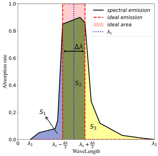
Figure 1.
Mathematical interpretation of PEF. represents the effective area in the target band. and represent the areas out of the target band, to the left and right of respectively.
FOM has been widely used to evaluate the thermal performance of TPV emitters [41,42,48,53]. However, it can be easily noticed that the ratio terms in FOM correspond to the same weight, which means even a high ratio in a rather short band could lead to a significant drop in FOM, particularly when optimizing in NIR. It is unreasonable that ratios in fairly short bands beyond the target range have the same effect as a high emissivity in the target band. One common practice to avoid the impact of ratios in a short band is to multiply a factor. However, this would raise a problem of tuning a new hyper-parameter. Therefore, compared to FOM, PEF could avoid the problem mentioned above due to its mathematical feature. Based on the waveform of target emissivity, PEF divides the emissivity spectrum into three parts. It can be easily observed from the definition that the larger the area of emissivity in the target band is the higher the value of PEF is (the better the performance of system is). Different from FOM, PEF measures the performance of TPV emitters at the level of geometric significance, which has nothing to do with the width and location of target band.
2.2. BOnSA Algorithm
Firstly, concerning the computation of spectral emissivity, we utilize the transfer-matrix method (TMM) [54], which has the following form:
where and represent the forward and backward waves of the electric field in the k-th layer. More details about TMM can be found in Appendix A. The reflectivity and transmissivity are then given by and , respectively. According to Kirchhoff’s law of thermal radiation [55], we have that , where is the absorptivity (the energy dissipation of scattering can be ignored).
Before proposing the algorithm, we show assumptions for our model. Firstly, the system is assumed to operate under suitable conditions ( K) and the refractive index of relevant materials is available for the corresponding situation. Secondly, we assume that the direction of the incident light is perpendicular to the plane of the thermal emitter. This can be achieved by appropriate design of the optical structure. We also assume that influences of the factors outside the given range of spectral emissivity can be neglected.
It is widely shared that SA can escape from local optima [56,57], which helps make up for the deficiency of BO, but requires a lengthy time to achieve theoretical convergence. Therefore, the speed of SA could be significantly improved via incorporating BO during its operation process. Nevertheless, the GP modeling strategy adopted by typical BO becomes a stumbling block for efficiency. A convincing reason for abandoning the conventional BO based on GP is exactly its huge cost of time and space.
Therefore, we introduce BO based on tree-structured parzen estimator (TPE) [58,59]. TPE divides the data into two categories with diverse density distributions, which are represented as follows:
TPE updates the agent model by Gaussian mixture clustering model (GMM) [60] and adopts Expected Improvement (EI). EI has the following form for the minimum [60]:
where and stands for the model-based algorithms approximation. Its solution for the minimum is . As for implementation, the algorithm has the setting of and . Due to its simplicity in contrast to GP, TPE not only runs faster and costs less, but also has excellent efficiency [60].
As illustrated in Figure 2, the SA executes the external epoch. In each epoch, the Metropolis algorithm [61,62] selects n layers to generate a new solution, which follows a uniform distribution. If the new solution is rejected, the algorithm will go to the next epoch, otherwise BOnSA will narrow down the scope and undergo multiple BOs. It turns out that the greater the PEF of a new solution is, the higher expectation of PEF in its neighborhood will be. Through computation accomplished by BO, BOnSA will probably reach local optima. In fact, to jump out of the local region, it is reasonable to end BO by continuing the next epoch. After applying SA, the so-called greedy search will traverse the materials from top to bottom, optimizing the thickness of each layer. Completing the procedure mentioned above, a fulfilling solution can be obtained eventually.
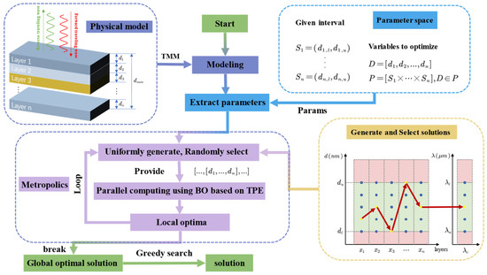
Figure 2.
Detailed description of BOnSA flow. In “Generate and Select solutions”, the circles represent solutions generated by means of a uniform distribution. The yellow circles represent the solutions that have been selected, while the blue circles are those that have not been selected during this process. The red arrows demonstrate a visual analogy of parameter selection in the optimization algorithm.
SA [45] and BO [41,42] have been applied to optimize the design of thermal emitters. However, both of them have their own disadvantages. We thus combine the two algorithms by taking advantage of the strengths of each one to develop a new optimization algorithm BOnSA, which uses SA for global optimization and BO for local optimization. BOnSA effectively averts SA from redundant global search and prevents BO from being stuck at a local optimum.
3. Results
3.1. Determination of the Material Structure
The fundamental structure of TPV thermal emitters is designed with two substructures, namely the anti-reflection substructure and the Fabry–Perot etalon. The main feature of the Fabry–Perot etalon is the two W layers on top and bottom, as well as materials in the middle, with low refractive index and almost zero extinction coefficient. A brief explanation is that the Fabry–Perot etalon has been proved to provide enhancement to the selectivity of a filter [63], which greatly increases the emissivity of the system in the target band. The additional anti-reflection substructure on its top plays a role in reducing the reflection of near-infrared light in the target band, which can be compared to a hat put on the Fabry–Perot etalon. For convenience, the anti-reflection substructure and Fabry–Perot etalon are abbreviatedly referred to as the hat substructure and FP substructure, respectively.
The overall process of determining the optimal material structure is displayed in Figure 3. In the fundamental structure, we take the combination of these candidates to form various hat substructures inspired by the periodic multilayer emitters and we choose the FP substructure which contains the periodic materials. Taking the ascending time cost into consideration, the basic unit of periodic materials is set to two, and materials are selected from the candidates as MgF2, ZnS, Si and SiO2. For all the possible fundamental structures, RS is performed to confirm the preliminary PEF of each one. Then sorted by the values of PEF, the substructures that appear with high frequencies in the front will be selected for further optimization. Eventually, through applying BOnSA, the optimal structure distinguishes itself in the last candidates.
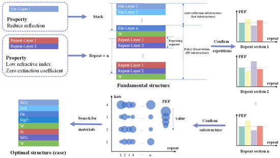
Figure 3.
The process of determining optimal structure.
As shown in Figure 4a, the values of PEF can reach a high level when the repetition of periodic materials in FP substructures equals 1. Additionally, one can obtain the number of layers in the anti-reflection substructure. It can also be observed that, in terms of the four layers on top of W, anti-reflective layers do perform better than others, due to its larger ranging space and higher maximal value of PEF. To sum up, the optimal fundamental structure can be expressed as {x1, x2, x3, x4, W, y1, y2, W}, where xj (for j = 1, 2, 3, 4) and yj (for j = 1, 2) denote different materials.
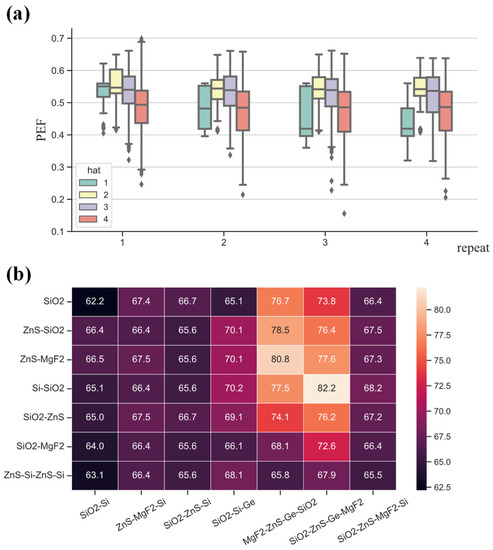
Figure 4.
(a) The boxplot of values of PEF corresponding to structures with different hats and repetition of periodic materials. (b) The heatmap of different FP substructures and hat substructures.
By analyzing the values of PEF with regard to different combinations, the material in each layer can now be confirmed. After applying BOnSA to optimize the structures, the values of PEF for all the combinations are shown in Figure 4b. Apparently, the structure corresponding to {SiO2, ZnS, Ge, MgF2} as the anti-reflection substructure and {W, Si, SiO2, W} as the Fabry–Perot etalon has the best performance with the maximal value of . As a result, one of the optimal structures is determined as {SiO2, ZnS, Ge, MgF2, W, Si, SiO2, W}. Please note that Ge has been added to the candidates for anti-reflection substructure. Many previous studies have shown that one of the good choices for fabrication of PV cells is Ge [64,65], which possesses the features of low bandwidth and high refractive index. According to Kirchhoff’s law of thermal radiation [55], Ge can help increase the emissivity (or absorptivity) of the target band, which has been verified by relevant experimentation [66]. Moreover, in analogy to Si, a material that can be used to build PV cells [67] and multilayer thermal emitters [68], we believe that Ge should also be a good candidate, the feasibility of which has indeed been supported by previous work [42,69]. Ge has also been proved to significantly improve the performance of thermal emitters in our work.
3.2. Performance of BOnSA
3.2.1. The Emission Spectrum of Different Optimal Structures
By employing BOnSA, the best optimal structure for a GaSb PV cell can be obtained in the above section, with the thickness of each layer being {140.0, 60.0, 129.6, 423.6, 10.5, 50.6, 8.4, 205.0} nm. As a complement, BOnSA is applied to another structure with great optimization potential, whose structure is confirmed as {MgF2, ZnS, Ge, SiO2, W, ZnS, SiO2, W} with thickness being {148.4, 59.1, 129.6, 403.3, 17.3, 93.2, 23.4, 201.6} nm. We also optimize the structures in the references [41,70] to see the performance of BOnSA proposed in this paper. The emission spectra of different structures are illustrated in Figure 5a.
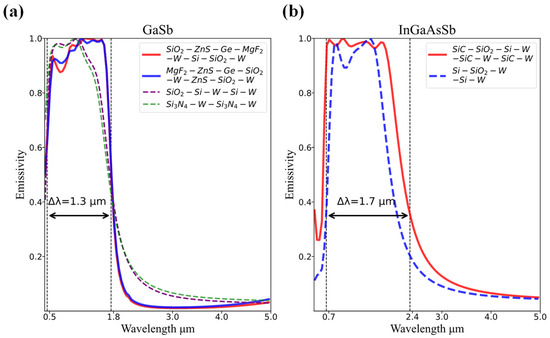
Figure 5.
The emission spectrum of different optimal structures including the optimization of the structures in [41,70] using BOnSA for GaSb PV cell (a) and for InGaAsSb PV cell (b).
In terms of GaSb PV cells, it is clear that the emissivity is lower in the band higher than , which can significantly reduce the thermalization loss of the TPV system. Moreover, in the required band , the emissivity curve of optimal structure can also maintain a steeper and plumper peak. According to Kirchhoff’s law of thermal radiation, low reflectivity can be obtained only in the target area, resulting in a higher emissivity. Generally, as shown by the solid line in Figure 5a, the shape of the curve in the target area is like a rectangular pulse, which is close to the desired one. Thus, it can be concluded that the structure proposed by us performs well in the target band. Similarly, BOnSA can also be employed to the structure designed for the InGaAsSb PV cell, which can be seen in Figure 5b. Compared to the structure obtained in the original paper [41], the emissivity of the optimal structure has relatively high values (nearly 1.0) via BOnSA in our paper with less fluctuation in the target band, which indicates the TPV thermal emitter can absorb as much energy as possible that can then be consumed by PV cells.
3.2.2. The Optimization Trajectories of BOnSA and Other Algorithms
The optimization process for one of the optimal structures ({SiO2, ZnS, Ge, MgF2, W, Si, SiO2, W}) is depicted in detail in Figure 6. Here the dots represent all the local PEF in trials and the lines stand for the historical optimal PEF. Based on the distribution histograms of PEF, the local optima generated by BOnSA is much better than GA and RS. Compared to BOnSA, although GA can give a global optimum, its efficiency is completely defeated by BOnSA since GA costs much more time.
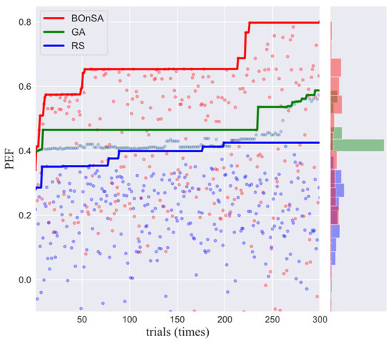
Figure 6.
The optimization trajectories using three different algorithms with their historical PEF distribution histograms.
In the early stage of optimization, BOnSA quickly reaches a temporary stable level, thanks to the boost via multiple BOs. The graph of historical optimal PEF has several ascending phases, resulting from the boost via BO in small regions. It can be understood in the sense that BO based on TPE can quickly approach the local optima, while SA will transfer from one area that may have been full excavated to another area to be exploited. In these simulations, it takes 3 to 5 min to obtain a good solution on our laptop (AN515-55-57C4, Acer, Inc., Suzhou, China), which also proves the efficiency of BOnSA.
3.2.3. Sensitivity Analysis
In terms of the sensitivity analysis in comparison to other work, BOnSA shows strong reliability.
As demonstrated in Figure 7, we analyze the sensitivity in our optimal structure by changing the thickness or varying the incident angle slightly. The gray area indicates the variation of emissivity when the thickness of one or more layers varies 1 to 3 nm, as a simulation of deviation that may arise in fabrication. Apparently, the slight change under the shadow almost does not affect its stability a little. Similarly, as the incident angle varies from 0 to 20°, the PEF value of the optimized structure changes by only , which illustrates the stability of the structure as well.
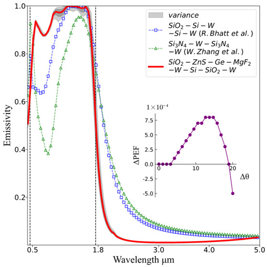
Figure 7.
Analysis of the emission spectrum regarding the optimal structure obtained via BOnSA in comparison with other works.
By contrast, BOnSA has also been applied to other structures designed for the GaSb PV cell, such as {Si3N4, W, Si3N4, W} [70] and {SiO2, Si, W, Si, W} [41]. As shown by the dotted lines in Figure 7, when it comes to the low band close to , a sharp decline appears and heavily affects the efficiency of the GaSb PV cell in the other two works. However, our approach can maintain a high PEF in the whole target band.
4. Discussion
4.1. Main Novelties
One of the reasons for the difference between our work and others lies in the choice of evaluator used in BOnSA. Although FOM is derived from the emission rate on average in the physical sense, shorter wavelength contributes less to the performance index, which leads to a shift to longer wavelength. However, PEF is derived according to the underlying mathematics that pays more attention to the entire region, which can overcome the above-mentioned shortcomings of FOM. This can be proved by applying BOnSA and PEF to the structures as shown in Figure 5a of our manuscript. By employing the optimization approach proposed in our work, the value of PEF for the {Si3N4, W, Si3N4, W} structure increases from 0.537 to 0.677, and PEF of {SiO2, Si, W, Si, W} structure increases from 0.374 to 0.642, where the corresponding thicknesses are {76.43, 12.14, 51.31, 180} nm and {108.57, 30, 15.71, 15.71, 200} nm, respectively.
Therefore, the results when using PEF and BOnSA are superior in NIR. It is worth mentioning that it takes merely several optimization steps to gain the optimal outcome.
In addition, our results possess merits in terms of multilayer structure design and optimization. In some previous work on multilayer thermal emitters, the elaboration of substructures has been given little attention. Meanwhile, regarding the optimization of material thicknesses in each layer, the majority of the previous work tend to use a single algorithm, which is demonstrated in Table 2.
Table 2.
Some previous studies of multilayer thermal emitters.
In contrast, the BOnSA algorithm proposed by us is a combination of two effective optimization algorithms. In particular, the epoch of SA is set to be a small finite value, which allows SA to find more local optima in a huge parameter space with reduced time cost. On this basis, BO searches for the global optimum in the neighborhood of local optima. Therefore, the two algorithms can cooperate together building on their respective strengths which leads to the optimization with better performance.
4.2. Mechanism Explanation
To explore the mechanism for the optimal structures for thermal emitters, we plot the normalized electric and magnetic field intensities. As illustrated in Figure 8a, the electric field is mainly concentrated in the layer of SiO2 and MgF2. The reason is that SiO2 on the top layer acts as an anti-reflection substructure to reduce the reflection in the range of target wavelengths.
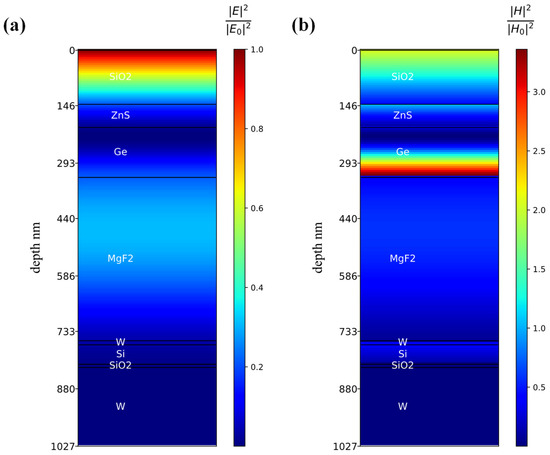
Figure 8.
(a,b) Contour of normalized electric and magnetic field intensities for our optimal structure.
What is more, it is obvious that a strong magnetic field enhancement exists in Ge as the third layer, as shown in the Figure 8b. The emissivity enhancement originates from localized modes, which are similar to the confined Tamm modes [37,38]. Tamm modes of multilayer structure exist inside a photonic band gap, and these modes localized at the surface are usually excited in the periodic system. It is exciting that Tamm modes can be observed inside the aperiodic multilayer structure. Together with the help of the Fabry–Perot etalon, the reflectivity and transmissivity can be sharply declined, and the emissivity can be improved in the visible light area and NIR. The optimal structure of TPV thermal emitters designed via BOnSA in turn helps us in understanding the selective thermal emission mechanism of aperiodic multilayered metamaterials better. Equipped with optimal TPV thermal emitters designed by BOnSA, the TPV systems can obtain high energy conversion efficiencies. Furthermore, the efficiencies in such systems based on near-field TPV can be further improved due to the near-field effects [73,74].
4.3. Calculation of Conversion Efficiency
We now calculate the conversion efficiency of TPV systems by the energy conversion relationship. The energy of the incident photon can be obtained by the emission spectrum of the following form:
The energy absorbed by the PV cell is given by
where is the emissivity of the structure, is the external quantum efficiency of GaSb PV cell and is the blackbody radiation intensity. Therefore, the conversion efficiency can be calculated as . With regard to the structures designed for GaSb cell, we have obtained the specific conversion efficiencies at 1200 K, as shown in Table 3.
Table 3.
Conversion efficiency of the system before and after optimization by BOnSA.
According to Table 3, it is obvious that by means of the optimization approach BOnSA, conversion efficiencies of the corresponding structures have been evidently improved in comparison to the original results in the references. Meanwhile, it can be seen that the selection of materials has a strong impact on the conversion efficiency.
Remark. It is undeniable that there are shortcomings of the algorithm BOnSA. Firstly, the results of the algorithm are partially dependent on the adjustment of the hyperparameters, which turns out to be tricky. Secondly, the emission spectra obtained by BOnSA are still depressed in some regions concerning the wavelength as shown in Figure 5. Though BOnSA can be further improved, it can be extended to solving related problems. For example, in general, in a problem where the physical model and the associated evaluator are known, BOnSA can be applied to seek for optimal parameters. It is promising that BOnSA may also be used to solve black-box problems.
5. Conclusions
In this paper, we propose a new evaluator PEF to replace FOM and employ BOnSA to carry on the design of TPV thermal emitters for GaSb PV cells as well as InGaAsSb PV cells. Through mathematical modeling and simulation, the optimal material structure for emitters with anti-reflection substructure and Fabry–Perot etalon presents excellent physical characteristics.
Following the rules given in this paper, the aperiodic multilayer structure with better performance can be designed by considering the optical properties of materials in simulations. Specifically, our optimal structure can be described as {SiO2, ZnS, Ge, MgF2, W, Si, SiO2, W}, with the corresponding thickness being {140.0, 60.0, 129.6, 423.6, 10.5, 50.6, 8.4, 205.0} nm, whose PEF reaches the value 0.822.
In addition, to demonstrate the robustness and reliability of such an approach, we apply BOnSA to other recent work on the structure design of TPV thermal emitters for GaSb PV cells. The numerical simulation shows that BOnSA leads to a better solution as the value of PEF is increased by more than 20% with less time cost. One can thus conclude that BOnSA has strong adaptability and a low calculation requirement.
Furthermore, with the help of normalized electric and magnetic field intensities, the mechanism of optimal TPV thermal emitters reveals the rationality of the structure from the underlying physics point of view.
In a word, through our optimization, we obtain optimal emitters with excellent optical characteristics, which can provide enlightening guidance for the construction of TPV thermal emitters.
Author Contributions
Conceptualization, Z.L.; methodology, Z.L. and Z.Z.; software, Z.Z.; validation, Z.Z.; formal analysis, Z.L.; resources, P.X.; data curation, P.X.; writing—original draft preparation, Z.L., Z.Z., P.X. and Z.M.; writing—review and editing, P.X. and Z.M.; visualization, Z.Z. and P.X.; supervision, Z.M.; project administration, Z.M.; funding acquisition, Z.M. All authors have read and agreed to the published version of the manuscript.
Funding
This research was funded by the National Natural Science Foundation of China, Grant Nos. 62173296 and 62003113.
Data Availability Statement
Publicly available datasets were analyzed in this study. This data can be found here: [RefractiveIndex.INFO—Refractive index database] (accessed on 15 March 2022).
Conflicts of Interest
The authors declare no conflict of interest.
Appendix A
To obtain the emission spectrum of an n-layer multilayer thermal emitter, we need to carry out the physical modeling and parameter calculation of our structure. Figure A1 shows the proposed structure with relevant important parameters.

Figure A1.
Schematic representation of multilayer structure. “1” and “n” correspond to the first and n-th layers respectively.
As for the calculation of the electromagnetic physical quantities in the model, one can adopt the transfer-matrix method (TMM) [54,75,76], finite difference time domain method (FDTD) [77] and the rigorous coupled-wave analysis method (RWCA) [78]. In this work, we perform TMM, which has the following total transmission moment of electric field amplitude [54]:
where and represent the forward and backward traveling waves of the electric field in the k-th layer, which can be vividly seen in Figure A1. As we are concerned with the interface in multilayers, the dynamical matrix of the j-th layer is denoted by . The product of dynamical matrices can be expressed as , and the propagation matrix of the j-th layer is denoted by . After applying matrix operations, we can obtain a transfer-matrix for the traveling waves. What is more, the reflectivity and transmissivity of the multilayer structure can be characterized by the parameters of the transfer-matrix. In addition, according to Kirchhoff’s law, we can obtain the emission spectrum of thermal emitters.
For the sake of standardization and clarity, we give the notations in this paper. As for an n-layer multilayer structure, () corresponds to the thickness of the j-th layer material. stands for the target bandwidth, and is the center wavelength of . represents the ensemble of parameters to be optimized, which spans the parameter space . It is not difficult to obtain the relation .
Appendix B
Python was chosen for realizing the algorithm in numerical simulations, which provides a wide variety of open-source and powerful packages such as NumPy [79] and SciPy [80]. As for the implement of BO, among several alternatives [81,82], we chose HyperOpt [83], due to its highly customized API and TPE approach.
In terms of hyper-parameters tuning for GaSb cell, the range for center wavelength is configured from 1.0 μm to 1.2 μm. Since when K, the band gap wavelength of GaSb cell μm. Thickness of each layer ranges from 5 nm to 305 nm. and are set to be 0.4 μm and 5 μm. Bandwidth is set to 1.3 μm.
The total epoch of SA is 400. Here, the convergence rate is removed from SA because it would take lengthy calculation time to reach the theoretical limit and it is replaced with , which means the algorithm will terminate if no better PEF appears after times. Additionally, the constant used to adjust the probability of acceptance is set to 0.4 here. With this setting for BO, BO will search around the local field with a certain size. The ratio of searching field to total space is written as , whose value is 0.1. For the sake of convenience, all the parameters considered in the optimization are listed in Table A1.
Table A1.
Physical and algorithmic parameters considered in this paper.
Table A1.
Physical and algorithmic parameters considered in this paper.
| Type | Title | Notation | Value |
|---|---|---|---|
| Physical | Center wavelength | Range from 1.0 to 1.2 μm | |
| Band gap wavelength of PV cell | μm (GaSb cell) | ||
| Lower bounds of emissivity | 0.4 μm | ||
| Upper bounds of emissivity | 5 μm | ||
| Bandwidth | 1.3 μm | ||
| Thickness of each layer | \ | Range from 5 to 305 nm | |
| Algorithmic | Total epoch of SA | \ | 400 |
| Epoch implementation Rate | 0.4 | ||
| Acceptance probability constant | 0.4 | ||
| Searching field ratio of BO | 0.1 |
References
- Wang, Q.; Zuo, W.; Cheng, M.; Deng, F.; Buja, G. Decoupled power control with indepth analysis of single-phase electric springs. IEEE Access 2020, 8, 21866–21874. [Google Scholar] [CrossRef]
- Mlangeni, S.; Ezugwu, A.E.; Chiroma, H. Deep Learning Model for Forecasting Institutional Building Energy Consumption. In Proceedings of the Conference on Information Communications Technology and Society (ICTAS), Durban, South Africa, 11–12 March 2020; IEEE: Piscataway, NJ, USA, 2020; pp. 1–8. [Google Scholar]
- Zhang, S. The Conquest of the Energy Kingdom. In Man-Made Sun; Springer: Berlin/Heidelberg, Germany, 2021; pp. 1–28. [Google Scholar]
- Reza, S.E.; Nitol, T.A.; Abd-Al-Fattah, I. Present scenario of renewable energy in Bangladesh and a proposed hybrid system to minimize power crisis in remote areas. Int. J. Renew. Energy Res. 2012, 2, 280–288. [Google Scholar]
- Laird, F.N.; Stefes, C. The diverging paths of German and United States policies for renewable energy: Sources of difference. Energy Policy 2009, 37, 2619–2629. [Google Scholar] [CrossRef]
- Bahadori, A.; Nwaoha, C. A review on solar energy utilisation in Australia. Renew. Sustain. Energy Rev. 2013, 18, 1–5. [Google Scholar] [CrossRef]
- Kannan, N.; Vakeesan, D. Solar energy for future world—A review. Renew. Sustain. Energy Rev. 2016, 62, 1092–1105. [Google Scholar] [CrossRef]
- Davies, P.; Luque, A. Solar thermophotovoltaics: Brief review and a new look. Sol. Energy Mater. Sol. Cells 1994, 33, 11–22. [Google Scholar] [CrossRef]
- Shockley, W.; Queisser, H.J. Detailed balance limit of efficiency of p-n junction solar cells. J. Appl. Phys. 1961, 32, 510–519. [Google Scholar] [CrossRef]
- Baranov, D.G.; Xiao, Y.; Nechepurenko, I.A.; Krasnok, A.; Alù, A.; Kats, M.A. Nanophotonic engineering of far-field thermal emitters. Nat. Mater. 2019, 18, 920–930. [Google Scholar] [CrossRef]
- Datas, A.; Algora, C. Detailed balance analysis of solar thermophotovoltaic systems made up of single junction photovoltaic cells and broadband thermal emitters. Sol. Energy Mater. Sol. Cells 2010, 94, 2137–2147. [Google Scholar] [CrossRef]
- Cuevas, J.C.; García-Vidal, F.J. Radiative heat transfer. ACS Photonics 2018, 5, 3896–3915. [Google Scholar] [CrossRef]
- Colodrero, S.; Mihi, A.; Häggman, L.; Ocana, M.; Boschloo, G.; Hagfeldt, A.; Miguez, H. Porous one-dimensional photonic crystals improve the power-conversion efficiency of dye-sensitized solar cells. Adv. Mater. 2009, 21, 764–770. [Google Scholar] [CrossRef]
- Zhou, Z.; Sakr, E.; Sun, Y.; Bermel, P. Solar thermophotovoltaics: Reshaping the solar spectrum. Nanophotonics 2016, 5, 1–21. [Google Scholar] [CrossRef]
- Ferguson, L.; Fraas, L. Theoretical study of GaSb PV cells efficiency as a function of temperature. Sol. Energy Mater. Sol. Cells 1995, 39, 11–18. [Google Scholar] [CrossRef]
- Torsello, G.; Lomascolo, M.; Licciulli, A.; Diso, D.; Tundo, S.; Mazzer, M. The origin of highly efficient selective emission in rare-earth oxides for thermophotovoltaic applications. Nat. Mater. 2004, 3, 632–637. [Google Scholar] [CrossRef] [PubMed]
- Bitnar, B.; Durisch, W.; Mayor, J.-C.; Sigg, H.; Tschudi, H. Characterisation of rare earth selective emitters for thermophotovoltaic applications. Sol. Energy Mater. Sol. Cells 2002, 73, 221–234. [Google Scholar] [CrossRef]
- Lin, S.-Y.; Moreno, J.; Fleming, J. Three-dimensional photonic-crystal emitter for thermal photovoltaic power generation. Appl. Phys. Lett. 2003, 83, 380–382. [Google Scholar] [CrossRef]
- Laroche, M.; Carminati, R.; Greffet, J.-J. Coherent thermal antenna using a photonic crystal slab. Phys. Rev. Lett. 2006, 96, 123903. [Google Scholar] [CrossRef]
- Liu, X.; Tyler, T.; Starr, T.; Starr, A.F.; Jokerst, N.M.; Padilla, W.J. Taming the blackbody with infrared metamaterials as selective thermal emitters. Phys. Rev. Lett. 2011, 107, 045901. [Google Scholar] [CrossRef]
- Veselago, V.G. Electrodynamics of substances with simultaneously negative and. Usp. Fiz. Nauk 1967, 92, 517. [Google Scholar] [CrossRef]
- Zhang, S.; Fan, W.; Panoiu, N.; Malloy, K.; Osgood, R.; Brueck, S. Experimental demonstration of near-infrared negative-index metamaterials. Phys. Rev. Lett. 2005, 95, 137404. [Google Scholar] [CrossRef]
- Zhang, X.; Zhang, S. Research advances in thermal metamaterials. Opto-Electron. Eng. 2017, 44, 49–63. [Google Scholar]
- Kadic, M.; Bückmann, T.; Schittny, R.; Wegener, M. Metamaterials beyond electromagnetism. Rep. Prog. Phys. 2013, 76, 126501. [Google Scholar] [CrossRef] [PubMed]
- Wang, H.; Sivan, V.P.; Mitchell, A.; Rosengarten, G.; Phelan, P.; Wang, L. Highly efficient selective metamaterial absorber for high-temperature solar thermal energy harvesting. Sol. Energy Mater. Sol. Cells 2015, 137, 235–242. [Google Scholar] [CrossRef]
- Jia, Y.; Wang, X.; Yin, H.; Yao, H.; Wang, J.; Fan, C. Highly tunable thermal emitter with vanadium dioxide metamaterials for radiative cooling. Appl. Opt. 2021, 60, 5699–5706. [Google Scholar] [CrossRef]
- Dyachenko, P.N.; Molesky, S.; Petrov, A.Y.; Störmer, M.; Krekeler, T.; Lang, S.; Ritter, M.; Jacob, Z.; Eich, M. Controlling thermal emission with refractory epsilon-near-zero metamaterials via topological transitions. Nat. Commun. 2016, 7, 11809. [Google Scholar] [CrossRef]
- Behera, S.; Joseph, J. Plasmonic metamaterial based unified broadband absorber/near infrared emitter for thermophotovoltaic system based on hexagonally packed tungsten doughnuts. J. Appl. Phys. 2017, 122, 193104. [Google Scholar] [CrossRef]
- Woolf, D.; Hensley, J.; Cederberg, J.; Bethke, D.; Grine, A.; Shaner, E. Heterogeneous metasurface for high temperature selective emission. Appl. Phys. Lett. 2014, 105, 081110. [Google Scholar] [CrossRef]
- Kudyshev, Z.A.; Kildishev, A.V.; Shalaev, V.M.; Boltasseva, A. Machine-learning-assisted metasurface design for high-efficiency thermal emitter optimization. Appl. Phys. Rev. 2020, 7, 021407. [Google Scholar] [CrossRef]
- Wilson, B.A.; Kudyshev, Z.A.; Kildishev, A.V.; Kais, S.; Shalaev, V.M.; Boltasseva, A. Metasurface design optimization via D-Wave based sampling. In Proceedings of the 2021 Conference on Lasers and Electro-Optics (CLEO), San Jose, CA, USA, 9–14 May 2021; IEEE: Piscataway, NJ, USA, 2021; pp. 1–2. [Google Scholar]
- Maremi, F.T.; Lee, N.; Choi, G.; Kim, T.; Cho, H.H. Design of multilayer ring emitter based on metamaterial for thermophotovoltaic applications. Energies 2018, 11, 2299. [Google Scholar] [CrossRef]
- Hou, G.; Wang, Q.; Zhu, Y.; Lu, Z.; Xu, J.; Chen, K. Tunable Narrowband Silicon-Based Thermal Emitter with Excellent High-Temperature Stability Fabricated by Lithography-Free Methods. Nanomaterials 2021, 11, 1814. [Google Scholar] [CrossRef]
- Kildishev, A.V.; Boltasseva, A.; Shalaev, V.M. Planar photonics with metasurfaces. Science 2013, 339, 1232009. [Google Scholar] [CrossRef] [PubMed]
- Sakurai, A.; Matsuno, Y. Design and fabrication of a wavelength-selective near-infrared metasurface emitter for a thermophotovoltaic system. Micromachines 2019, 10, 157. [Google Scholar] [CrossRef] [PubMed]
- Li, W.; Guler, U.; Kinsey, N.; Naik, G.V.; Boltasseva, A.; Guan, J.; Shalaev, V.M.; Kildishev, A.V. Refractory plasmonics with titanium nitride: Broadband metamaterial absorber. Adv. Mater. 2014, 26, 7959–7965. [Google Scholar] [CrossRef] [PubMed]
- Sakr, E.; Zhou, Z.; Bermel, P. High efficiency rare-earth emitter for thermophotovoltaic applications. Appl. Phys. Lett. 2014, 105, 111107. [Google Scholar] [CrossRef]
- Chen, W.; Liu, J.; Ma, W.-Z.; Yu, G.-X.; Chen, J.-Q.; Cai, H.-Y.; Yang, C.-F. Numerical study of multilayer planar film structures for ideal absorption in the entire solar spectrum. Appl. Sci. 2020, 10, 3276. [Google Scholar] [CrossRef]
- Shuai, Y.; Tan, H.; Liang, Y. Polariton-enhanced emittance of metallic–dielectric multilayer structures for selective thermal emitters. J. Quant. Spectrosc. Radiat. Transf. 2014, 135, 50–57. [Google Scholar] [CrossRef]
- Wu, J.; Wu, F.; Zhao, T.; Antezza, M.; Wu, X. Dual-band nonreciprocal thermal radiation by coupling optical Tamm states in magnetophotonic multilayers. Int. J. Therm. Sci. 2022, 175, 107457. [Google Scholar] [CrossRef]
- Zhang, W.; Wang, B.; Zhao, C. Selective thermophotovoltaic emitter with aperiodic multilayer structures designed by machine learning. ACS Appl. Energy Mater. 2021, 4, 2004–2013. [Google Scholar] [CrossRef]
- Sakurai, A.; Yada, K.; Simomura, T.; Ju, S.; Kashiwagi, M.; Okada, H.; Nagao, T.; Tsuda, K.; Shiomi, J. Ultranarrow-band wavelength-selective thermal emission with aperiodic multilayered metamaterials designed by Bayesian optimization. ACS Cent. Sci. 2019, 5, 319–326. [Google Scholar] [CrossRef]
- Babiker, S.G.; Shuai, Y.; Sid-Ahmed, M.O.; Xie, M. One-dimensional multilayer microstructure emitter for thermophotovoltaic applications. Int. J. Energy Inf. Commun. 2014, 5, 9–20. [Google Scholar] [CrossRef]
- Langlais, M.; Bru, H.; Ben-Abdallah, P. High temperature layered absorber for thermo-solar systems. J. Quant. Spectrosc. Radiat. Transf. 2014, 149, 8–15. [Google Scholar] [CrossRef]
- Liang, H.; Lai, J.; Zhou, Z. Ultra-narrowband infrared thermal emitter based on Fabry–Perot-like vacuum resonance cavity. J. Opt. A Pure Appl. Opt. 2009, 11, 105001. [Google Scholar] [CrossRef]
- Cai, H.; Sun, Y.; Wang, X.; Zhan, S. Design of an ultra-broadband near-perfect bilayer grating metamaterial absorber based on genetic algorithm. Opt. Express 2020, 28, 15347–15359. [Google Scholar] [CrossRef] [PubMed]
- Silva-Oelker, G.; Jerez-Hanckes, C.; Fay, P. High-temperature tungsten-hafnia optimized selective thermal emitters for thermophotovoltaic applications. J. Quant. Spectrosc. Radiat. Transf. 2019, 231, 61–68. [Google Scholar] [CrossRef]
- Akhtar, S.; Khan, M.N.; Kurnia, J.C.; Shamim, T. Investigation of energy conversion and flame stability in a curved micro-combustor for thermo-photovoltaic (TPV) applications. Appl. Energy 2017, 192, 134–145. [Google Scholar] [CrossRef]
- Simovski, C.; Maslovski, S.; Nefedov, I.; Tretyakov, S. Optimization of radiative heat transfer in hyperbolic metamaterials for thermophotovoltaic applications. Opt. Express 2013, 21, 14988–15013. [Google Scholar] [CrossRef]
- Hatakeyama-Sato, K.; Kashikawa, T.; Kimura, K.; Oyaizu, K. Tackling the challenge of a huge materials science search space with quantum-Inspired annealing. Adv. Intell. Syst. 2021, 3, 2000209. [Google Scholar] [CrossRef]
- Wu, J.; Chen, X.-Y.; Zhang, H.; Xiong, L.-D.; Lei, H.; Deng, S.-H. Hyperparameter optimization for machine learning models based on Bayesian optimization. J. Electron. Sci. Technol. 2019, 17, 26–40. [Google Scholar]
- Shahriari, B.; Swersky, K.; Wang, Z.; Adams, R.P.; De Freitas, N. Taking the human out of the loop: A review of Bayesian optimization. Proc. IEEE 2015, 104, 148–175. [Google Scholar] [CrossRef]
- Akhtar, S.; Kurnia, J.C.; Shamim, T. A three-dimensional computational model of H2–air premixed combustion in non-circular micro-channels for a thermo-photovoltaic (TPV) application. Appl. Energy 2015, 152, 47–57. [Google Scholar] [CrossRef]
- Katsidis, C.C.; Siapkas, D.I. General transfer-matrix method for optical multilayer systems with coherent, partially coherent, and incoherent interference. Appl. Opt. 2002, 41, 3978–3987. [Google Scholar] [CrossRef] [PubMed]
- Pigeat, P.; Rouxel, D.; Weber, B. Calculation of thermal emissivity for thin films by a direct method. Phys. Rev. B 1998, 57, 9293. [Google Scholar] [CrossRef]
- Koulamas, C.; Antony, S.; Jaen, R. A survey of simulated annealing applications to operations research problems. Omega 1994, 22, 41–56. [Google Scholar] [CrossRef]
- Eglese, R.W. Simulated annealing: A tool for operational research. Eur. J. Oper. Res. 1990, 46, 271–281. [Google Scholar] [CrossRef]
- Schulz, E.; Speekenbrink, M.; Krause, A. A tutorial on Gaussian process regression: Modelling, exploring, and exploiting functions. J. Math. Psychol. 2018, 85, 1–16. [Google Scholar] [CrossRef]
- Quinonero-Candela, J.; Rasmussen, C.E. A unifying view of sparse approximate Gaussian process regression. J. Mach. Learn. Res. 2005, 6, 1939–1959. [Google Scholar]
- Bergstra, J.; Bardenet, R.; Bengio, Y.; Kégl, B. Algorithms for hyper-parameter optimization. In Proceedings of the 24th International Conference on Neural Information Processing Systems (NIPS’11), Granada, Spain, 12–15 December 2011; Curran Associates Inc.: Red Hook, NY, USA, 2011; pp. 2546–2554. [Google Scholar]
- Beichl, I.; Sullivan, F. The metropolis algorithm. Comput. Sci. Eng. 2000, 2, 65–69. [Google Scholar] [CrossRef]
- Haario, H.; Saksman, E.; Tamminen, J. An adaptive Metropolis algorithm. Bernoulli 2001, 7, 223–242. [Google Scholar] [CrossRef]
- Otaka, M.; Takahashi, S.; Utaka, K.; Horita, M.; Yazaki, T. Fundamental evaluation of semiconductor waveguide-type in-line wavelength selective filter with Fabry-Perot etalon resonator. In Proceedings of the 2001 International Conference on Indium Phosphide and Related Materials, 13th IPRM (Cat. No. 01CH37198), Nara, Japan, 14–18 May 2001; IEEE: Piscataway, NJ, USA, 2001; pp. 170–173. [Google Scholar]
- Gamel, M.M.A.; Jern, K.P.; Rashid, W.E.; Yau, L.K.; Jamaludin, M.Z. The effect of illumination intensity on the performance of germanium based-thermophotovoltaic cell. In Proceedings of the 2019 IEEE Regional Symposium on Micro and Nanoelectronics (RSM), Putrajaya, Malaysia, 21–23 August 2019; IEEE: Piscataway, NJ, USA, 2019; pp. 129–132. [Google Scholar]
- Dhass, A.D.; Kumar, R.S.; Lakshmi, P.; Natarajan, E.; Arivarasan, A. An investigation on performance analysis of different PV materials. Mater. Today Proc. 2020, 22, 330–334. [Google Scholar] [CrossRef]
- Zulkefle, A.A.; Zainon, M.; Zakaria, Z.; Sopian, K.; Amin, N. Numerical modeling of silicon/germanium (Si/Ge) superlattice solar cells. In Proceedings of the 7th WSEAS International Conference on. Renewable Energy Sources (RES ‘13), Kuala Lumpur, Malaysia, 2–4 April 2013; p. 233. [Google Scholar]
- Han, J.; Lu, L.; Yang, H. Numerical evaluation of the mixed convective heat transfer in a double-pane window integrated with see-through a-Si PV cells with low-e coatings. Appl. Energy 2010, 87, 3431–3437. [Google Scholar] [CrossRef]
- Khorrami, Y.; Fathi, D. Broadband thermophotovoltaic emitter using magnetic polaritons based on optimized one-and two-dimensional multilayer structures. JOSA B 2019, 36, 662–666. [Google Scholar] [CrossRef]
- Tong, J.K.; Hsu, W.-C.; Huang, Y.; Boriskina, S.V.; Chen, G. Thin-film ‘thermal well’emitters and absorbers for high-efficiency thermophotovoltaics. Sci. Rep. 2015, 5, 10661. [Google Scholar] [CrossRef] [PubMed]
- Bhatt, R.; Kravchenko, I.; Gupta, M. High-efficiency solar thermophotovoltaic system using a nanostructure-based selective emitter. Sol. Energy 2020, 197, 538–545. [Google Scholar] [CrossRef]
- Wang, H.; Alshehri, H.; Su, H.; Wang, L. Design, fabrication and optical characterizations of large-area lithography-free ultrathin multilayer selective solar coatings with excellent thermal stability in air. Sol. Energy Mater. Sol. Cells 2018, 174, 445–452. [Google Scholar] [CrossRef]
- Liu, G.; Xuan, Y.; Han, Y.; Li, Q. Investigation of one-dimensional si/sio2 hotonic crystals for thermophotovoltaic filter. Sci. China Ser. E Technol. Sci. 2008, 51, 2031–2039. [Google Scholar] [CrossRef]
- Zhang, W.B.; Zhao, C.Y.; Wang, B.X. Enhancing near-field heat transfer between composite structures through strongly coupled surface modes. Phys. Rev. B 2019, 100, 075425. [Google Scholar] [CrossRef]
- Zhang, W.B.; Wang, B.X.; Zhao, C.Y. Active control and enhancement of near-field heat transfer between dissimilar materials by strong coupling effects. Int. J. Heat Mass Tran. 2022, 188, 122588. [Google Scholar] [CrossRef]
- Mohammed, Z.H. The Fresnel Coefficient of Thin Film Multilayer Using Transfer Matrix Method TMM; IOP Conference Series: Materials Science and Engineering; IOP Publishing: Bristol, UK, 2019; p. 032026. [Google Scholar]
- Carrera-Escobedo, V.H.; Rosu, H.C. Electromagnetic transmittance in alternating material-metamaterial layered structures. Rev. Mex. Física 2017, 63, 402–410. [Google Scholar]
- Tran, A.M.; Houshmand, B.; Itoh, T. Analysis of electromagnetic coupling through a thick aperture in multilayer planar circuits using the extended spectral domain approach and finite difference time-domain method. IEEE Trans. Antennas Propag. 1995, 43, 921–926. [Google Scholar] [CrossRef]
- Moharam, M.; Pommet, D.A.; Grann, E.B.; Gaylord, T. Stable implementation of the rigorous coupled-wave analysis for surface-relief gratings: Enhanced transmittance matrix approach. JOSA A 1995, 12, 1077–1086. [Google Scholar] [CrossRef]
- Harris, C.R.; Millman, K.J.; van der Walt, S.J.; Gommers, R.; Virtanen, P.; Cournapeau, D.; Wieser, E.; Taylor, J.; Berg, S.; Smith, N.J.; et al. Array programming with NumPy. Nature 2020, 585, 357–362. [Google Scholar] [CrossRef] [PubMed]
- Virtanen, P.; Gommers, R.; Oliphant, T.E.; Haberland, M.; Reddy, T.; Cournapeau, D.; Burovski, E.; Peterson, P.; Weckesser, W.; Bright, J. SciPy 1.0: Fundamental algorithms for scientific computing in Python. Nat. Methods 2020, 17, 261–272. [Google Scholar] [CrossRef] [PubMed]
- Ueno, T.; Rhone, T.D.; Hou, Z.; Mizoguchi, T.; Tsuda, K. COMBO: An efficient Bayesian optimization library for materials science. Mater. Discov. 2016, 4, 18–21. [Google Scholar] [CrossRef]
- Martinez-Cantin, R. BayesOpt: A Bayesian optimization library for nonlinear optimization, experimental design and bandits. J. Mach. Learn. Res. 2014, 15, 3735–3739. [Google Scholar]
- Bergstra, J.; Yamins, D.; Cox, D. Making a Science of Model Search: Hyperparameter Optimization in Hundreds of Dimensions for Vision Architectures. PMLR: Proceedings of Machine Learning Research. In Proceedings of the 30th International Conference on Machine Learning, Atlanta, Atlanta, GA, USA, 16–21 June 2013; Sanjoy, D., David, M., Eds.; Volume 28, pp. 115–123. [Google Scholar]
Disclaimer/Publisher’s Note: The statements, opinions and data contained in all publications are solely those of the individual author(s) and contributor(s) and not of MDPI and/or the editor(s). MDPI and/or the editor(s) disclaim responsibility for any injury to people or property resulting from any ideas, methods, instructions or products referred to in the content. |
© 2022 by the authors. Licensee MDPI, Basel, Switzerland. This article is an open access article distributed under the terms and conditions of the Creative Commons Attribution (CC BY) license (https://creativecommons.org/licenses/by/4.0/).