Article

Indirect Thermographic Temperature Measurement of a Power-Rectifying Diode Die

by
Krzysztof Dziarski
1,*,
Arkadiusz Hulewicz
2,
Grzegorz Dombek
1 and
Łukasz Drużyński
1
1
Institute of Electric Power Engineering, Poznan University of Technology, Piotrowo 3A, 60-965 Poznan, Poland
2
Institute of Electrical Engineering and Electronics, Poznan University of Technology, Piotrowo 3A, 60-965 Poznan, Poland
*
Author to whom correspondence should be addressed.
Energies 2022, 15(9), 3203; https://doi.org/10.3390/en15093203
Submission received: 28 March 2022 / Revised: 23 April 2022 / Accepted: 25 April 2022 / Published: 27 April 2022

Abstract

:
This article concerns the indirect thermographic temperature measurement of a die of the semiconductor diode D00-250-10. The article shows how the goal was achieved. The methodology of selecting the point at which thermographic measurements of the temperature of the diode cases were performed is discussed. The method of thermographic measurement of the case temperature and the measuring system used is described. The method of simulations making it possible to obtain the die’s temperature on the basis of thermographic casing temperature measurement is presented. In order to enable a better understanding of the discussed issues, the construction of the diode used and the heat flow equation are described. As a result of the work carried out, the point at which the temperature is closest to the die temperature was indicated on the diode case. It is shown that the difference between the casing temperature and the die temperature does not exceed 2 °C at the point indicated. An indirect measurement of the die’s temperature is carried out for different values of the power dissipated on the die.

1. Introduction

One of the most important issues related to the operation of semiconductor elements is the measurement of their die’s temperature. Information about the die temperature is needed in order to use the semiconductor element in such a way that the circuit of which it is a part works properly. Semiconductor elements are widely used in technical fields, in particular in electronics [1,2]. Their main tasks include rectifying the alternating current. The need to convert alternating current to direct current also occurs when the current value is high [3]. This phenomenon occurs, for example, in AC/DC/AC, AC/DC, and DC/AC high power-converter systems (kVA) [4]. In turn, high power-converter systems are used, inter alia, in the automotive industry (electromobility) [5], renewable energy sources [6], and in the cross-border transmission of electricity [7].
One of the most important issues related to the operation of semiconductor elements is the measurement of their die’s temperature. Information about the die temperature is needed in order to use the semiconductor element in such a way that the circuit of which it is a part works properly. Semiconductor elements are widely used in technical fields, in particular in electronics and power electronics [1,2].
One of the main tasks of semiconductor elements is to rectify alternating current. The need to convert alternating current to direct current also appears when the current value is high [3]. This phenomenon occurs, for example, in high-power AC/DC/AC, AC/DC, and DC/AC converter systems (in the order of thousands of voltamps) [4].
In turn, high-power converter systems are used, among others, in the automotive industry (e.g., in the construction of electric car chargers) [5], renewable energy sources (change of the current and voltage parameters generated in wind turbines and photovoltaic panels to parameters consistent with the grid parameters) [6], and in cross-border transmission of electricity (when the voltage parameters in the power system of one country differ from those of the other country) [7].
One of the semiconductor elements used to build high-power converter systems is a rectifying diode. The operation of the diode using the properties taken into account during the design process determines the correct operation of the converter system [8]. The most commonly used materials for the production of power diodes are silicon (Si) [9] and silicon carbide (SiC) [10]. SiC diodes are characterized by a wider band gap, greater thermal resistance, and lower switching losses [11]. However, such a diode is much more expensive than a diode made of Si. For this reason, despite inferior parameters, Si diodes are also used.
Heat in semiconductor elements appears as a result of their power losses [12]. Additional factors contributing to the increase in semiconductor temperature are the processes of the hole and electron recombination in the area of the semiconductor junction and switching losses [13]. The temperature of the semiconductor element is also influenced by the external temperature [14]. Semiconductor elements work properly when the semiconductor crystal (die) works at the appropriate temperature (about 70 °C)—in this case, the diode properties (e.g., the values of switching frequency, transistor amplifications, and voltage drops at the diode semiconductor junctions) are consistent with the values selected by the designer.
As the temperature of the diode increases, the graph of the current I flowing through the diode as a function of the voltage at the diode terminals V (I = f (V)) changes. As a consequence, the properties of the diode (e.g., the V value) change. For this reason, the knowledge of the die temperature of the semiconductor diode reveals the function I = f (V) of the rectifier diode. The properties of this diode are also known. Another negative effect of the operation of semiconductor matrices at excessive temperatures is their shorter service life and greater susceptibility to damage [15,16]. This is connected with higher costs due to the more frequent replacement of diodes.
An accurate understanding of the die temperature of a semiconductor diode operating in a prototype electronic circuit may have another economic benefit, which is a precise heat sink. Due to the power dissipated in power electronic systems, a large heat sink is used. The selection of a smaller heat sink with the proven cooling efficiency of the semiconductor diode die would reduce the final costs of the manufactured device. Circuits that allow the temperature of the power semiconductor diode to be determined by indirect thermal imaging temperature measurement can be part (node) of the IoT (Internet of Things). Such a system may be one of the solutions implemented as part of Industry 4.0.
As the matrix is placed inside the case of the semiconductor element, direct measurement of the die temperature is difficult. Opening the housing will change the operating and cooling conditions. The heat generated in the semiconductor diode die will be transferred directly to the air. For this reason, the die temperature measured with the case opened will differ from the die temperature measured with the housing closed [17]. It should be noted that semiconductor devices are made of metal or plastic, and they are constructed in such a way that they are destroyed upon opening. For this reason, direct temperature measurement is associated with irreversible damage to the element [18]. Such an element cannot be reused in a constructed system.
An alternative to impractical direct measurement is indirect measurement. Indirect measurement is the calculation of the die temperature from the housing temperature. The case temperature can be measured using the tactile or non-tactile method. The former method is based on the use of a temperature sensor, such as a resistor with a known resistance value at a certain temperature, a thermistor, and a thermocouple [19].
The use of a temperature sensor placed in an overly large case (compared to the housing of a semiconductor element) may disturb the temperature distribution in the case of the semiconductor element. As a consequence, the measured temperature value may differ significantly from the actual temperature. Another problem to be solved is the difficulty of determining thermal resistance between the sensor case and the semiconductor case. It depends on, inter alia, the force with which the sensor housing is applied to the semiconductor case, the size of the contact area between the two cases, and the adhesion of both cases.
The above-mentioned problems can be solved with the help of thermal imaging. Due to the high values of the current conducted through the diode, the safer method is thermographic measurement [20], which is non-contact. There is then no need to touch the diode case, which reduces the risk of electric shock. However, correct thermographic temperature measurement of the power semiconductor diode housing is not problem-free [21]. Power diode cases are often made of metal, with a low value of the emissivity factor ε (ε < 0.2 for a temperature of 20–150 °C) and a high value of the reflectance factor ρ. Additionally, the diode housing has the shape of a cylinder, thanks to which the thermographic measurement of the surface temperature may be affected by an error related to the change in angular emissivity as a function of the viewing angle [22,23,24,25].
The problem of determining the die temperature on the basis of the case temperature has been addressed in various ways. There are known methods of measuring the thermal resistance of the Rthj-c junction case [26]. Additionally, applications of the Cauer [27] and Foster [28] methods are known for modeling the heat flow path on the junction–case route. Fourier transform was also used to simplify the equations [29]. Models of 1-D [30] and 3-D [31] temperature distribution have been proposed. There is also a known method of thermal impedance reconstruction in a heat source based on the measurement of IR radiation on the surface of an electronic device [32]. Thermal imaging temperature measurements were taken of LEDs and electronic components placed in TO-220 cases [33].
The research results found in the literature were not sufficient to achieve the goal of indirect thermal imaging of the die temperature of the power semiconductor diode D00-250-10 (IF = 250 A, UFM = 1.5 V). The research work found concerned the measurement of a die temperature in the TO 220 [34] and TO 247 [35] cuboidal casings and concerned elements used in lower power systems. The methodology of thermographic temperature measurement presented therein differs from the methodology of thermographic measurement of cylindrical housings: in the case of cuboidal housings, the angular emissivity does not need to be taken into account. It should be noted that the TO 220 and TO 247 cases were made of a polymer with a high ε value. The case of the D00-250-10 diode was shaped like a cylinder. It was also made of metal, which offers a low ε value.
No papers were found where the temperature of the power diode was determined on the basis of thermovision measurement of the housing temperature. For this reason, we decided to take this measurement. To accomplish this, the following steps were taken:
-
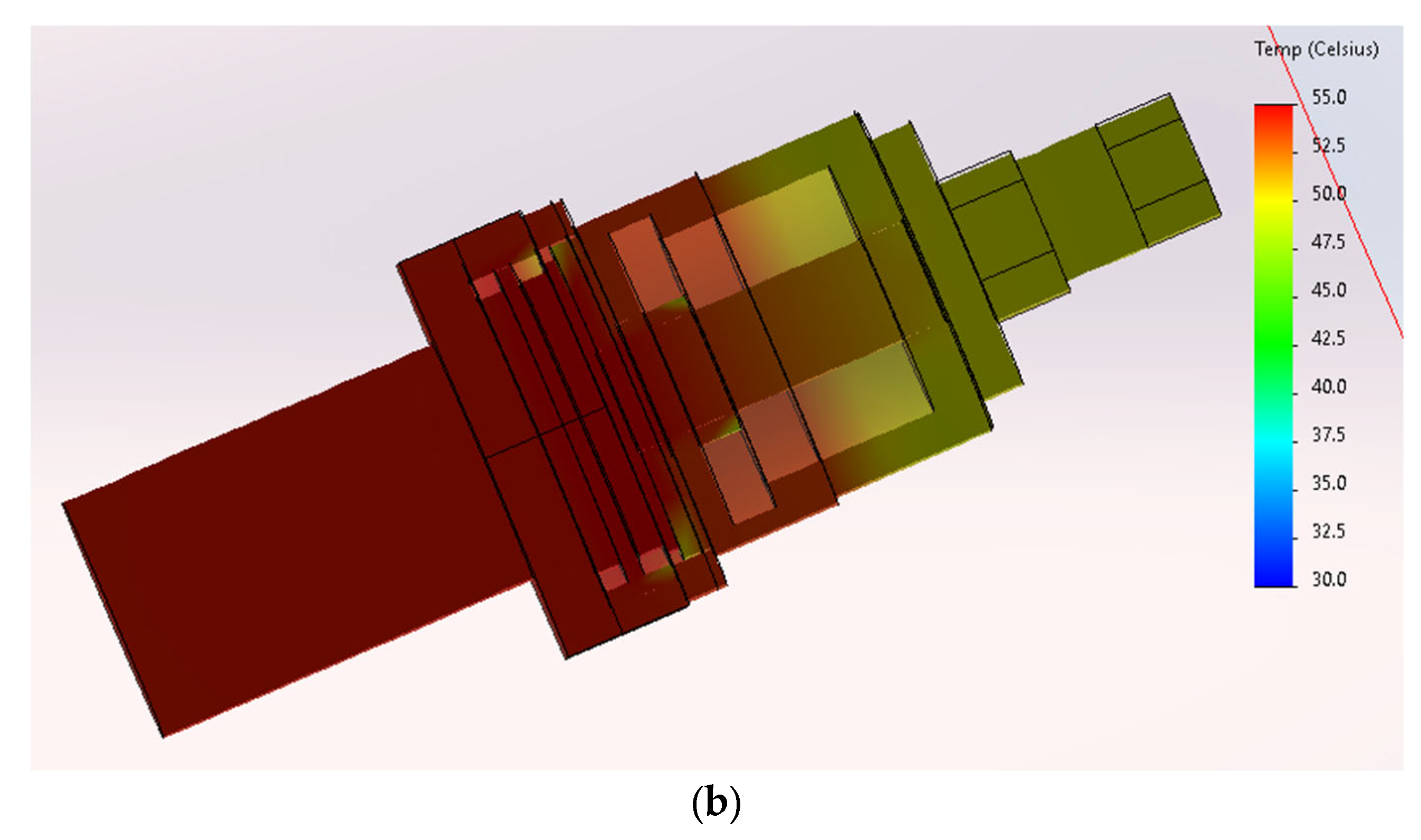
A thermogram of the power diode housing and thermogram of the diode of the power semiconductor diode were made, and the values of the power dissipated on the diode of the semiconductor diode were measured;
-
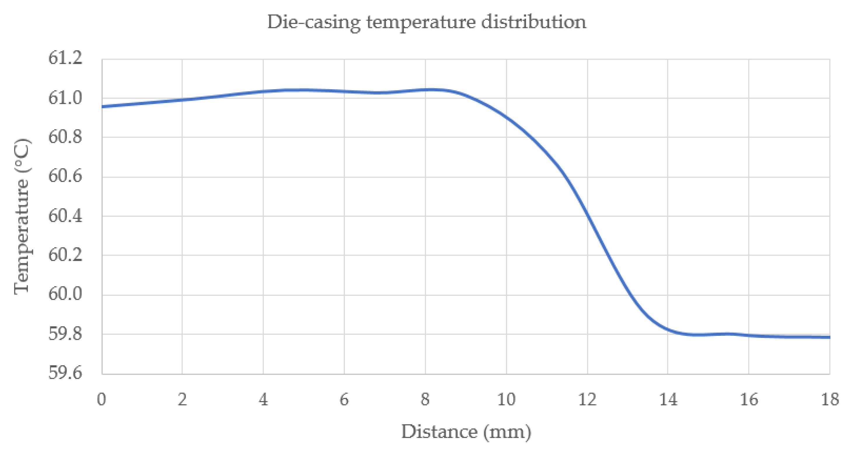
We found a point on the power diode housing where the housing temperature was closest to the die temperature;
-
A simulation of the temperature distribution in the power diode housing was run. On the basis of the performed measurements and simulations, we checked how much the diode temperature differed from the temperature at the designated point of the housing.

2. Materials and Methods

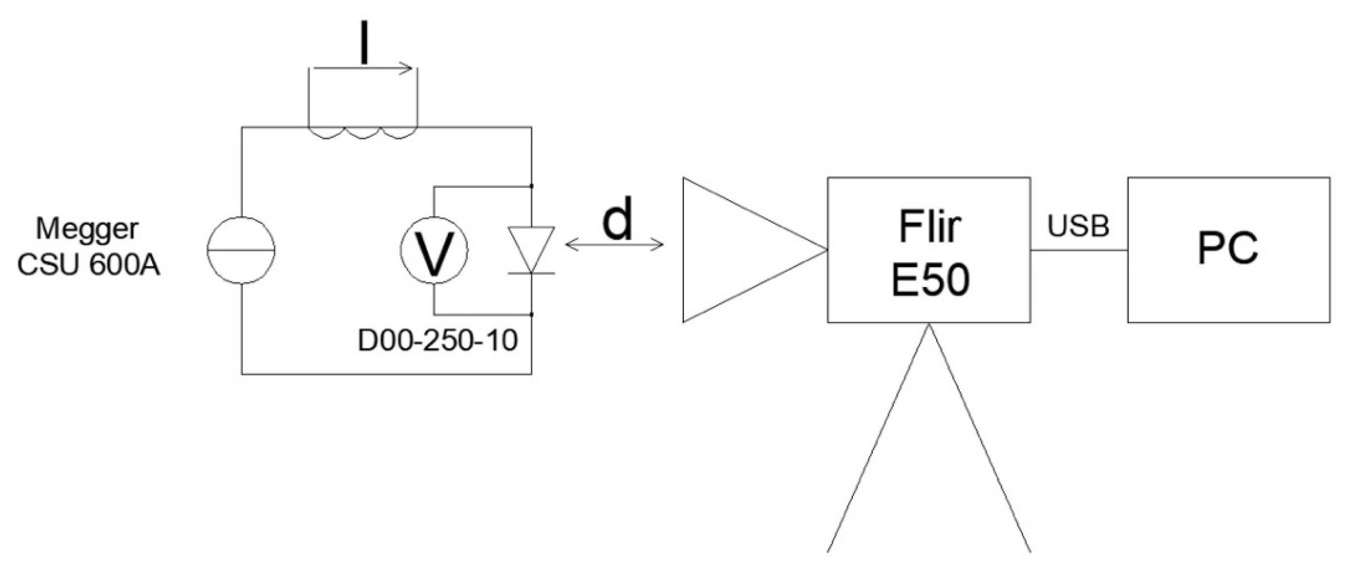
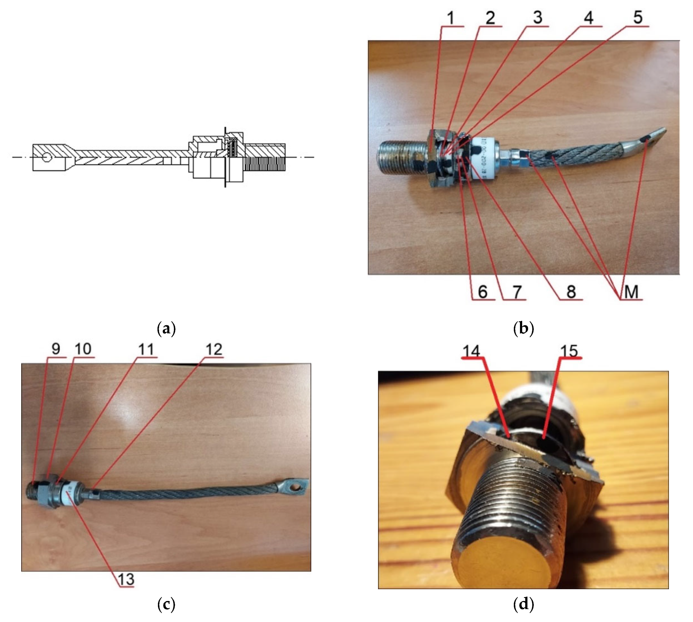
2.1. Measurement System

Performing an indirect thermovision die temperature measurement requires the knowledge of temperature distribution in the case where the die is placed. The knowledge of this distribution makes it possible to find points on the casing whose temperature is closest to the die temperature. Determination of the temperature distribution in the case also makes it possible to determine the difference between the die temperature and the temperature of a selected point on the case [18,19].
In order to find the points whose temperature is closest to the die temperature, experimental work was carried out. The performed works consisted of performing thermovision temperature measurements of selected surfaces of the D00-250-10 diode (Lamina, Piaseczno, Poland) (IF = 250A, UF = 1.5 V). Thermovision measurements of the temperature of selected diode surfaces were made. The temperature of the outer and inner surfaces of the diode was measured.
The thermovision measurement of the surface temperature required the knowledge of the ε coefficient of this surface. A large part of the D00-250-10 diode case was made of metal. The ε value of the part of the diode made of plastic and the part of the diode made of a material resembling porcelain was also unknown. For this reason, markers were made on the observed surfaces, with the use of Velvet Coating 811-21 paint with a specific emissivity coefficient value ranging from 0.970 to 0.975 for temperatures from −36 °C to 82 °C [20]. The diode, the placement of markers, and the numbers of the observed surfaces are shown in Figure 1.
The observed diodes (closed and opened) were placed alternately in the system consisting of the CSU 600A power source (Megger, Dover, England) and the Flir E50 thermal imager (Flir, Wilsonville, OR, USA). The thermal imager was connected via USB interface to a laptop equipped with Flir Tools software. The schematic diagram of the measurement system is shown in Figure 2.
Four series of measurements were performed during the research. During the measurements in a given series, the value of the current I flowing through the junction was kept constant. The current value was measured with a UT-201 multimeter (UNI-T, Dongguan City, China). At the same time, thermovision temperature measurements of the selected surface of the diode case were taken. When it was noticed that the difference between the consecutive recorded temperature values was less than the measurement error of the thermal imager (2 °C or 2% of reading, for ambient temperature, whichever is greater) in the arbitrarily assumed time of 10 min, the temperature was considered to be steady. Thermograms were made for the established temperature of the observed surface, and the values of I = 7.5 A, I = 10 A, I = 12.5 A, and I = 15 A.

2.2. Determination of Simulation Parameters
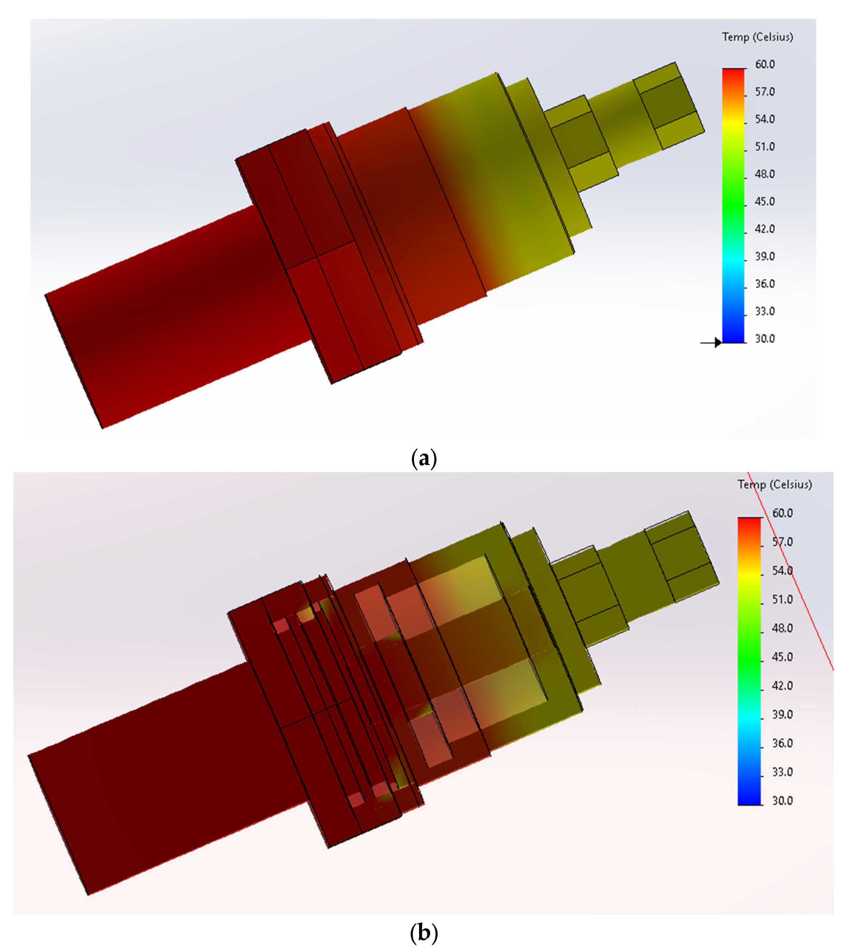
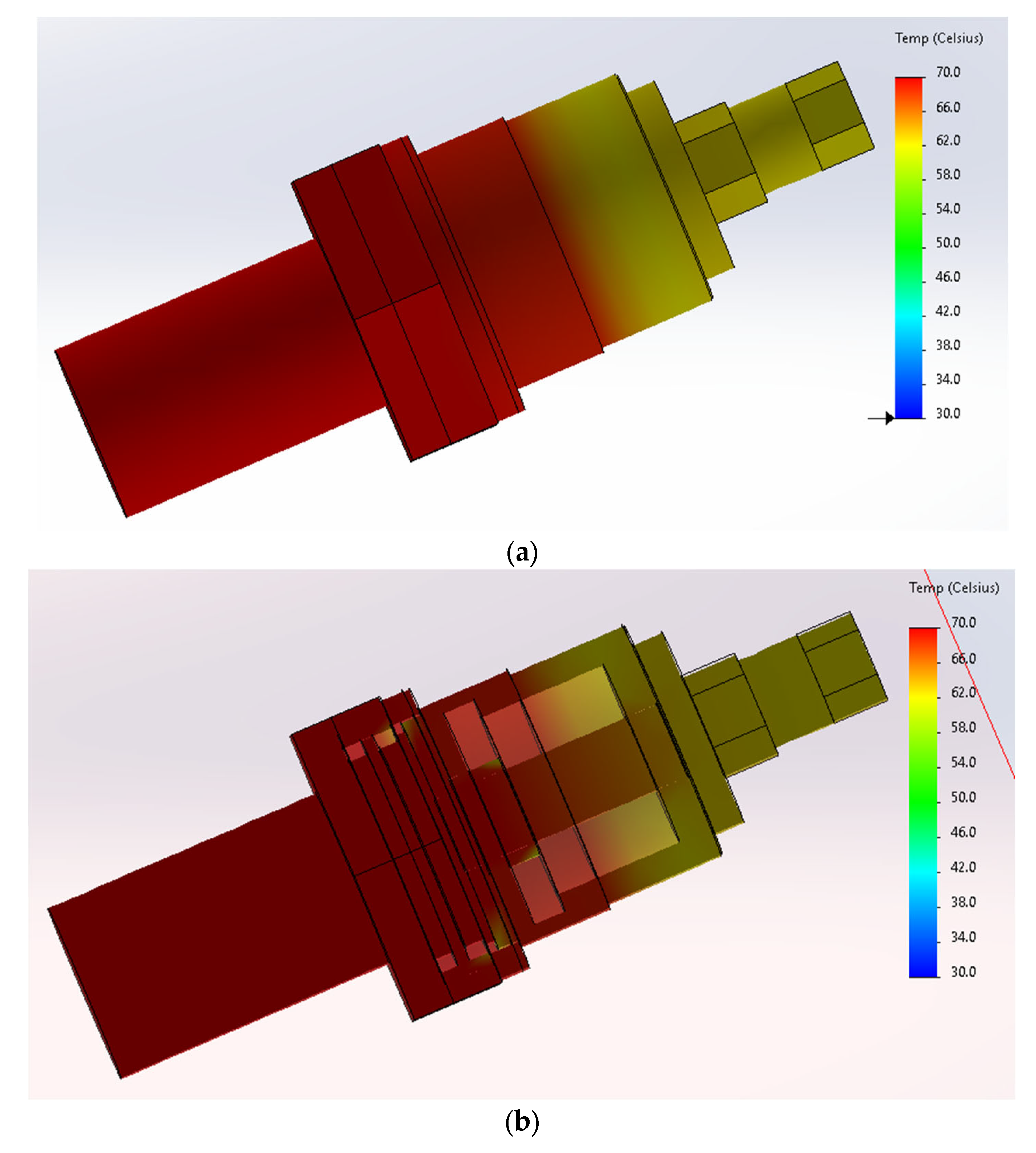
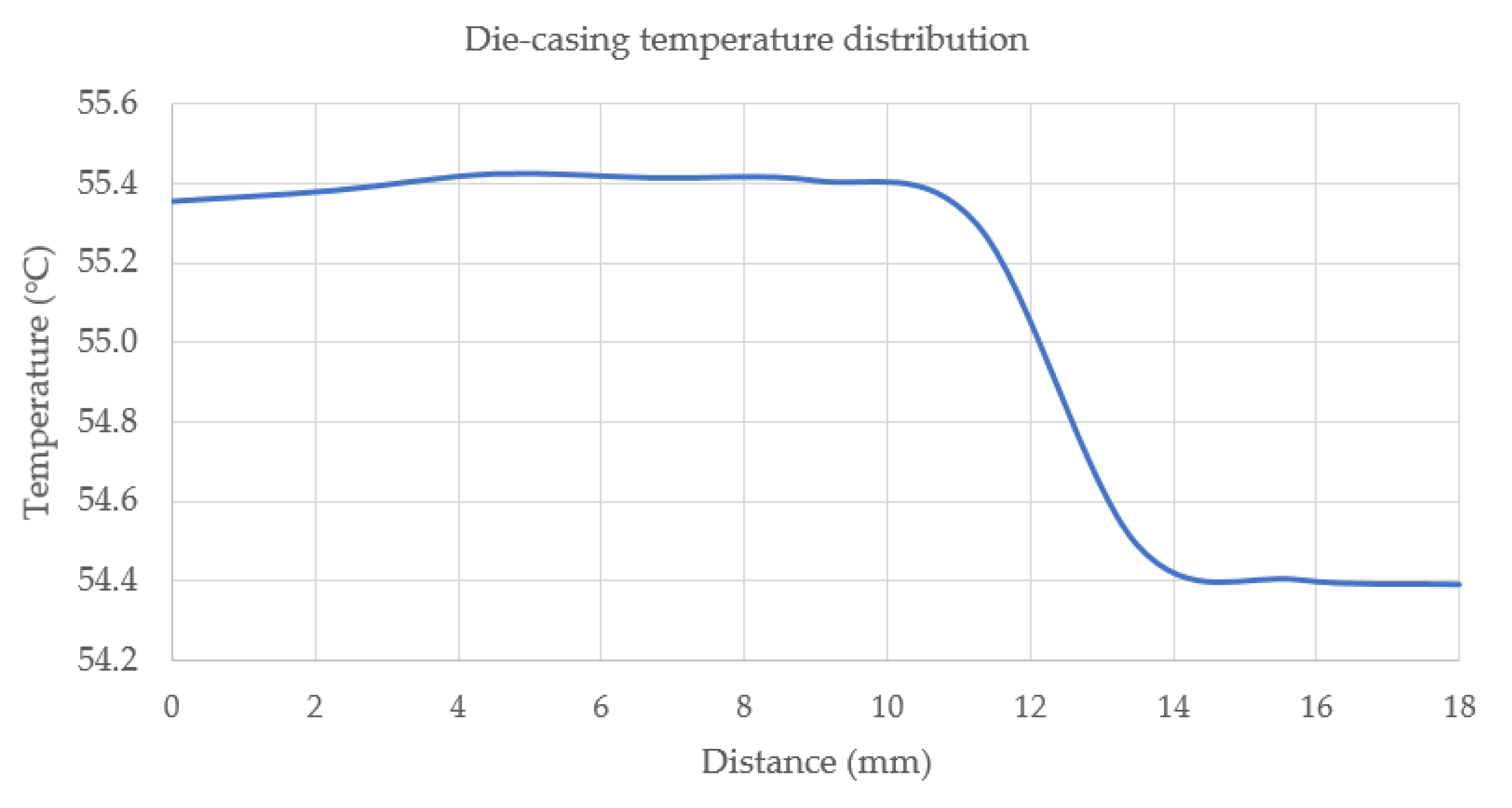
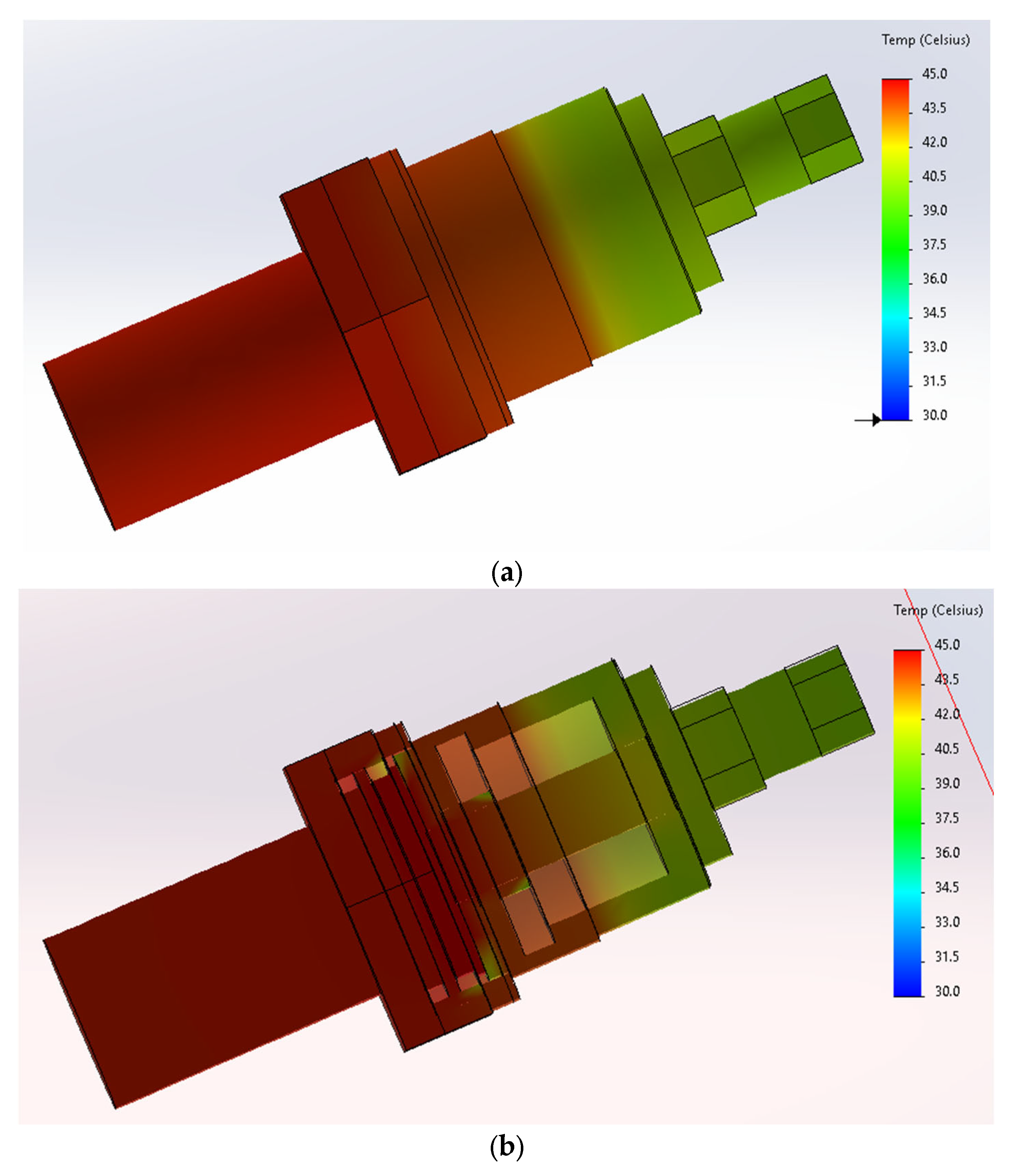
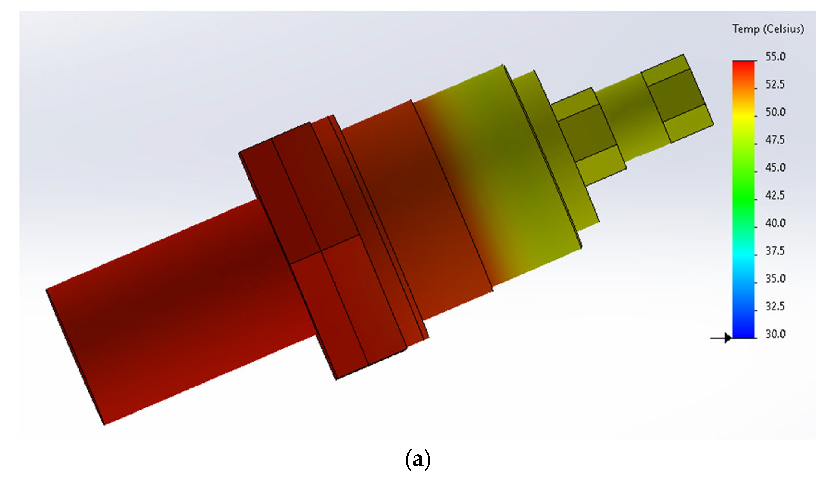
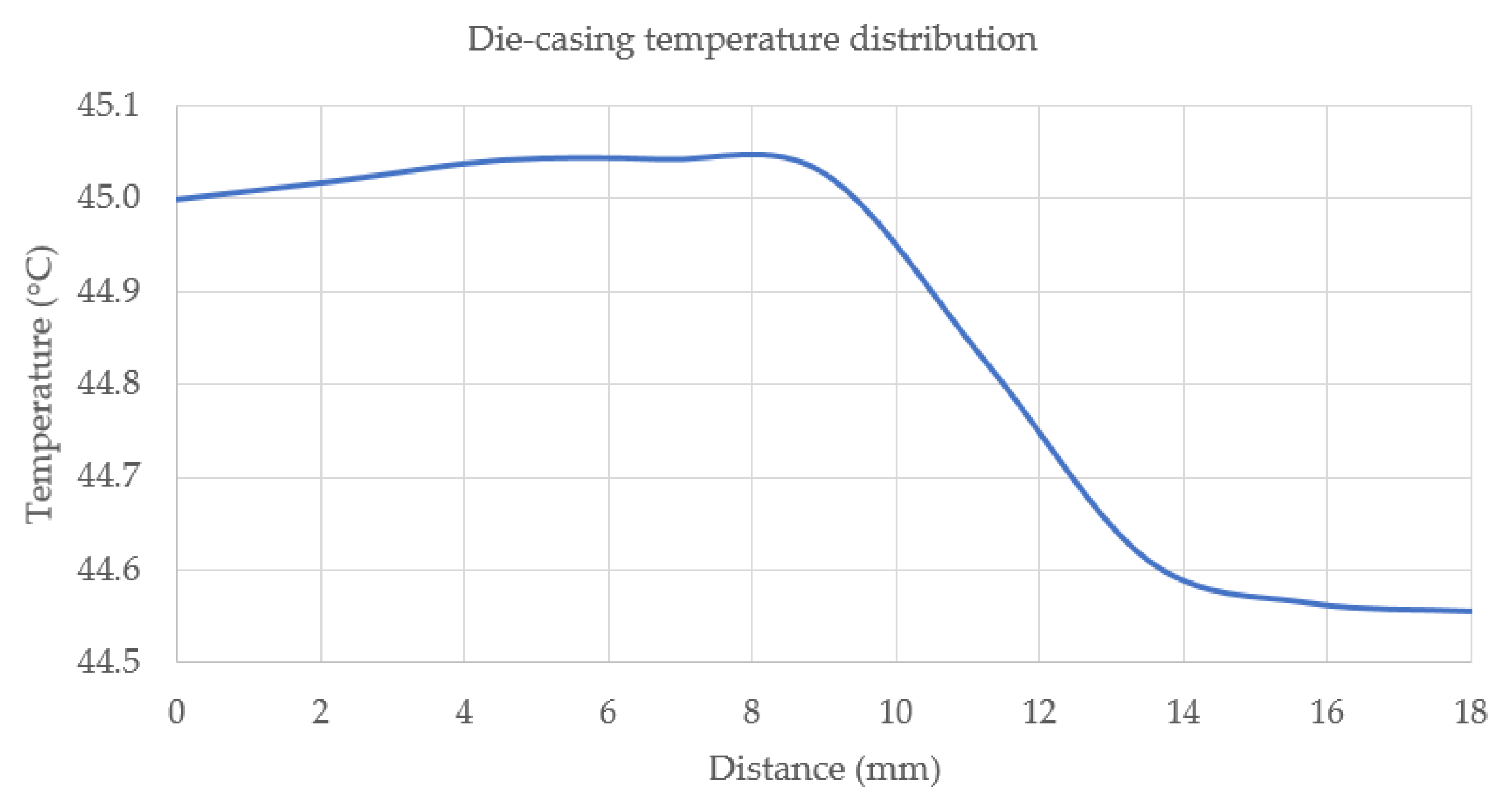
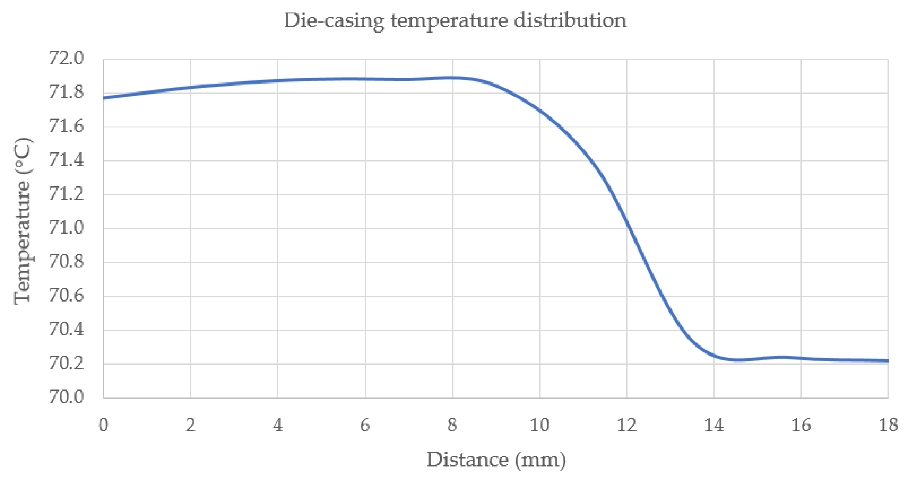
The transient heat transfer in the steady state can be described by Fourier’s law [22]:
J = k T
where ∇T is a gradient of the temperature in (K).
Equation (2) can be written in the following form:
J = k T x
where x is the distance between the points where the temperature values of die and diode case were measured (m), and J is a radiative heat flux (W∙m−2).
After separating the variables and integrating Equation (2) on both sides, the time constant can be obtained from the following boundary conditions:
for   x = 0 T = T 1 for   x = x k T = T 2
where xk is the end point of the analyzed heat flow path (m), T1 is the temperature at the starting point of the analyzed heat flow path (K), and T2 is the temperature at the end point of the analyzed heat flow path (K).
After determining the time constant, when J penetrates the entire wall, Equation (3) takes the form of Equation (4):
T 1 T 2 = P c S k x k
where Pc is the total power applied to the wall (W) and S (m2) is the area of the wall penetrated by J [W∙m−2].
Analyzing Equation (4), it can be seen that the value of the temperature difference between two points of the casing depends on the power Pc applied to the casing, the geometry of the analyzed part of the casing, and the material properties of the analyzed part of the casing (k value).
Equation (4) is easy to apply for single elements with simple geometry. In the case of elements with complex geometry, fragments of which are made of different materials, numerical methods can be used. One of them is the FEA (Finite Element Analysis) method. By definition, FEA is a numerical method for solving problems in engineering and mathematical physics [24].
The software applied in the work performed was Solidworks 2020 SP05 (Dassault Systèmes, Vélizy-Villacoublay, France), which uses FEA. Using this software, simulation work was completed. Performing the simulation work required creating a model of the observed diode. For this purpose, the observed diode was dimensioned to the nearest 1 mm.
Determining temperature distribution in the case using Solidworks requires the knowledge of the power dissipated at the PN Pj junction, the value of the convection coefficient hc, the value of the radiation coefficient hr, and thermal conductivity.
The value of Pj was determined on the basis of the measurements performed, as the product of I flowing through the observed diode, the measured voltage drop at the diode terminals Vd, and the cosine of the phase shift cosφ between I and Vd.
The cosφ value was determined experimentally. The resistance R, capacitance C, and the inductance L of the diode were measured using an LCR HM 8118 bridge (Hameg, Mainhausen, Germany). Based on the measured values of L and C, the reactance X of the diode was determined. The value of φ was obtained as the arctangent of the quotient of X and R. It was assumed that the entire power dissipated at the PN junction of the diode was converted into thermal losses.
The values of the current measurement error ΔI and the voltage drop measurement error at the diode terminals ΔVd were determined in accordance with the UT55 multimeter manual (UNI-T, Dongguan City, China). The measurement error of the power dissipated at the junction ΔPj was determined using the following formula [25]:
Δ P j = Δ I V d + Δ V d I
The hr coefficient defines the amount of thermal energy transferred to the environment by radiation per unit time, per unit area, per unit temperature difference between the body radiating energy and the environment. The hr value can be determined using equation [26]:
h r = ε σ c ( T S + T a ) ( T S 2 + T a 2 )
where σc is Stefan–Boltzmann constant equal to 5.67 × 10⁻⁸ (W∙m−2∙K−4)), TS is the surface temperature (K), and Ta is the air temperature (K).
In the case of Solidworks software, the hr value is calculated on the basis of the equation implemented in the software and the ε value of the surface entered by the user. In the conducted works, the ε values of individual parts of the case were selected on the basis of the comparative method.
It was assumed that the temperature values measured on the markers (Figure 1) are true values. The temperature of each of the selected fragments was measured by observing the marker with the chosen value of ε = 0.97. After each temperature measurement, the position of the observed point was changed. The point closest to the marker was observed. The value of ε was selected until the measured temperature values were the same.
The hc coefficient was selected using the theory of similarity to physical phenomena. Relationships with physical quantities characterizing a given phenomenon were described using the criteria of Nusselt, Grashof, and Prandtl.
The value of hcr for a cylindrical surface can be determined by the following equation [27]:
h c r = 0.48 ( g P r α d 3 ν 2 ( T s T a ) ) 1 4 k d r
where hcr is the convection coefficient of the cylindrical surface (W∙m−2∙K−1), g is the gravitational acceleration of 9.8 (m∙s−2), dr is equal to the work roll diameter (a characteristic size in this case) (m), Pr is the Prandtl number (–), α is a coefficient of expansion equal to 0.0034 (K−1), and ν is kinematic viscosity equal to 1.9 × 10⁻⁵ (m2∙s−1).
The Prandtl number can be found using the following equation [28]:
P r = c η k
where c is the specific heat of air equal to 1005 (J∙kg−1∙K−1) in 293.15 (K), η is dynamic air viscosity equal to 1.75 × 10⁻⁵ (kg∙m−1∙s−1) in 273.15 (K).
In the case of flat surfaces, the value of hc can be determined using the following equation [29]:
h c f = N u k L
where hcf is the convection coefficient of flat surfaces, Nu is the Nusselt number (-), and L is the characteristic length in meters (for a vertical wall, it is its height).
The Nusselt number can be determined from the following equation [30]:
N u = a ( P r G r ) b
where a and b are dimensionless coefficients, the values of which depend on the shape and orientation of the analyzed surface and the product Pr × Gr, and Gr is the Grashof number.
The Grashof number is described by the following equation [31]:
G r = α g ( T S T a ) ρ 2 L 3 η 2
where ρ is air density equal to 1.21 (kg∙m−3) in 273.15 (K).
The values of the a and b coefficients from Equation (10) depend on the shape and orientation of the heat transferring surface. The values of the a and b coefficients are presented in Table 1.
When analyzing Equation (5), it can be noticed that in order to determine the temperature distribution, it is necessary to know the value of the specific thermal conductivity coefficient k. As the metal alloys from which the diode case was made were not exactly known, the values of coefficient k were determined by simulation. Knowing the temperature values on the diode surfaces, the power dissipated at the junction and the values of convection and radiation coefficients, the k values were selected so that the simulation results were consistent with the results of thermovision measurements of the temperature of the diode case and the connector (Figure 1). On the basis of the selected values of the thermal conductivity coefficient k, the material from which the given surface was used was identified.

3. Results

Conducting a simulation in Solidworks requires the knowledge of the values of hcf, hcr, and ε coefficients, and the power dissipated at the connector. The parameters used in the simulation are shown in Table 2, Table 3, Table 4 and Table 5.
As a result of the simulations, temperature distributions were obtained, as shown in Figure 3, Figure 4, Figure 5 and Figure 6.
The obtained values of the differences between the simulated die temperature and the casing point (Figure 1) are presented in Table 6.
The correctness of the results obtained in the simulation was verified by comparing the results of thermographic measurements of the case temperature. The comparison is presented in Table 7.
As a result of the simulations, information was obtained on the temperature distribution on the surface of the D00-250-10 diode case and inside the case. Consequently, it was possible to find a point on the surface of the case where the temperature measured by thermo-vision was closest to the die temperature. The case of the D00-250-10 diode is cylindrical, and it thus differs from the case of the power semiconductor elements analyzed so far. The work carried out did not focus on determining the parameters of the predetermined heat flow path. As a result of the simulations, the temperature was determined as a function of the distance between the die of the semiconductor diode and the point on the housing, the temperature of which is closest to the die temperature. The obtained results are shown in Figure 7, Figure 8, Figure 9 and Figure 10.
The acquired knowledge about the temperature distribution in the D00-250-1 diode case, the selection of the measurement point, and the differences between the die temperature and the temperatures of individual points are useful during diagnostic work.

4. Discussion

The operating temperature of the junction of semiconductor elements is a significant parameter ensuring their reliable work. Its value provides important diagnostic information, but its direct measurement is difficult and, in many cases, even impossible. A solution to this problem is the use of thermal imaging to assess the junction temperature. As an auxiliary tool, an assessment of the junction temperature based on the results of mathematical simulations was proposed.
The main purpose of the research presented in this article was to check whether thermal imaging measurements of the semiconductor housing could be useful in assessing the temperature of its junction. In order to determine the optimal measurement point, appropriate simulations were carried out in Solidworks software, the reliability of which was confirmed by thermographic measurements. Thanks to the simulation work, it was possible to select the optimal measurement point at which the smallest temperature difference appeared between that point and the semiconductor junction. To carry out the simulation, it was necessary to determine the coefficients of the materials from which the diode was made. The values of these coefficients proposed by the authors were confirmed by comparing the simulation results for different powers of the joint with the results of thermographic measurements.
It is worthwhile noting that in the case of using the simulation results, it is possible to carry out thermographic measurements at an appropriately selected point, as a result of which the error in the assessment of the semiconductor junction temperature will have the lowest values. As already mentioned, the obtained results of the temperature simulation of the analyzed surfaces were compared with the temperature determined by other methods. As a result of these works, it was noticed that the values of the appearing discrepancies did not exceed the measurement error of the measuring instrument.
Due to this regularity, the combination of simulation methods and thermographic measurements seems to be a useful tool in assessing the temperature of a semiconductor junction on the basis of thermographic measurements of its housing. The analysis of thermographic measurements and the results of simulation tests confirmed these conclusions. At the same time, the results of the work confirmed the thermal differentiation in the analyzed points of the support, which, if incorrectly selected, may be a source of additional errors. As predicted and according to simulation results, the diode housing wall indicated in this study turned out to be the best measurement area. This correctness was confirmed for different powers emitted at the semiconductor junction of the diode.

5. Conclusions

Semiconductor elements are important parts of converter systems. Their proper work determines the correct operation of the converter system and its lifetime. The semiconductor elements work properly when the die temperature inside the case is not excessive.
It can be dangerous to measure the temperature of a power semiconductor diode encased in a metal housing with a sensor held against it. The risk of electric shock can be eliminated with the use of thermal imaging.
It is impossible to perform a direct thermographic measurement of the die as it is placed inside the case. Instead, indirect thermographic measurement of the die temperature can be performed. This is a measurement where the die temperature is judged from the temperature of the case.
A large part of the diode case is made of metal, a material with a low value of the emissivity factor ε. For this reason, when performing indirect thermographic die temperature measurement, the ε coefficient of the observed surface should be increased, e.g., by painting it black. The shape of the observed surface is by no means insignificant. In the case of thermographic temperature measurement of a cylindrical surface, it should be remembered that the value of ε changes with the change of the viewing angle.
Analyzing the data in Table 6, three points on the D00-250-10 diode case can be selected: points 9, 10, and 11 (Figure 1). It is difficult to perform a thermographic temperature measurement in step 9 because it is a thread placed in the radiator. The differences between the die temperature and the temperature of point 10 turned out to be smaller than the differences between the die temperature and the temperature of point 11. In addition, the case wall of the diode D00-250-10 at point 10 is flat. This makes it easier to choose the right angle of observation. For this reason, it should be considered that point 10 is the most suitable for making an indirect thermographic measurement of the die temperature. It was shown that at the indicated point, the difference between the casing temperature and the die temperature did not exceed 2 °C.
The presented results can be deployed in the course of other works to be pursued in the future. One example is the development of a system for continuous indirect thermovision temperature measurement of the die of semiconductor elements. Such a system could be part of the Internet of Things (IoT) node.

Author Contributions

K.D.; methodology, K.D. and A.H.; formal analysis, K.D. and A.H.; investigation, K.D., A.H., and Ł.D.; resources, K.D.; writing—original draft preparation, K.D., A.H., Ł.D., and G.D.; writing—review and editing, K.D., A.H., Ł.D., and G.D.; visualization, K.D.; supervision, K.D. and A.H. All authors have read and agreed to the published version of the manuscript.

Funding

This research was funded by the Ministry of Education and Science of Poland, grant numbers 0212/SBAD/0542 and 0711/SBAD/4561.

Institutional Review Board Statement

Not applicable.

Informed Consent Statement

Not applicable.

Conflicts of Interest

The authors declare no conflict of interest.

References

  1. Juneja, S.; Pratap, R.; Sharma, R. Semiconductor technologies for 5G implementation at millimeter wave frequencies–Design challenges and current state of work. Eng. Sci. Technol. Int. J. 2021, 24, 205–217. [Google Scholar] [CrossRef]
  2. Torzyk, B.; Więcek, B. Vector Analysis of Electrical Networks for Temperature Measurement of MOS Power Transistors. Pomiary Autom. Robot. 2021, 25, 83–87. [Google Scholar] [CrossRef]
  3. Xu, S.; Zhang, L.; Ding, W.; Guo, H.; Wang, X.; Wang, Z.L. Self-doubled-rectification of triboelectric nanogenerator. Nano Energy 2019, 66, 104165. [Google Scholar] [CrossRef]
  4. Felinto, A.S.; Jacobina, C.B.; Fabricio, E.L.L.; de Lacerda, R.P. Six-Leg Three-Phase AC–DC–AC Converter with Shared Legs. IEEE Trans. Ind. Appl. 2021, 57, 5227–5238. [Google Scholar] [CrossRef]
  5. Amiri, p.; Eberle, D.; Gautam, D.; Botting, C. A CCM Bridgeless Single-Stage Soft-Switching AC-DC Converter for EV Charging Application. In Proceedings of the 2021 IEEE Energy Conversion Congress and Exposition (ECCE), Vancouver, BC, Canada, 10–14 October 2021; pp. 1846–1852. [Google Scholar] [CrossRef]
  6. Nakamura, Y. Electrothermal Cosimulation for Predicting the Power Loss and Temperature of SiC MOSFET Dies Assembled in a Power Module. IEEE Trans. Power Electron. 2020, 35, 2950–2958. [Google Scholar] [CrossRef]
  7. Van Erp, R.; Soleimanzadeh, R.; Nela, L. Co-designing electronics with microfluidics for more sustainable cooling. Nature 2020, 585, 211–216. [Google Scholar] [CrossRef]
  8. Hulewicz, A.; Dziarski, K.; Dombek, G. The Solution for the Thermographic Measurement of the Temperature of a Small Object. Sensors 2021, 21, 5000. [Google Scholar] [CrossRef]
  9. Kałuża, M.; Więcek, B.; De Mey, G.; Hatzopoulos, A.; Chatziathanasiou, V. Thermal impedance measurement of integrated inductors on bulk silicon substrate. J. Microelectron. Reliability 2017, 73. [Google Scholar] [CrossRef]
  10. Więcek, B.; De Mey, G. Thermovision in Infrared–Basics and Applications; Measurement Automation Monitoring Publishing House: Warszawa, Poland, 2011. [Google Scholar]
  11. Minkina, W.; Dudzik, S. Infrared Thermography: Errors and Uncertainties; John Wiley & Sons: Hoboken, NJ, USA, 2009. [Google Scholar]
  12. Jung, G. A low-power embedded poly-Si micro-heater for gas sensor platform based on a FET transducer and its application for NO2 sensing. Sens. Actuators B Chem. 2021, 334, 129642. [Google Scholar] [CrossRef]
  13. Moure, A. In situ thermal runaway of Si-based press-fit diodes monitored by infrared thermography. Results Phys. 2020, 19, 103529. [Google Scholar] [CrossRef]
  14. Kandeal, A.W. Infrared thermography-based condition monitoring of solar photovoltaic systems: A mini review of recent advances. Sol. Energy 2021, 223, 33–43. [Google Scholar] [CrossRef]
  15. Aumeunier, M.H. Infrared thermography in metallic environments of WEST and ASDEX Upgrade. Nucl. Mater. Energy 2021, 26, 100879. [Google Scholar] [CrossRef]
  16. Dziarski, K.; Hulewicz, A.; Dombek, G.; Frąckowiak, R.; Wiczyński, G. Unsharpness of Thermograms in Thermography Diagnostics of Electronic Elements. Electronics 2020, 9, 897. [Google Scholar] [CrossRef]
  17. Nishi, K. Research on Package Thermal Resistance of Power Semiconductor Devices. In Proceedings of the 35th Semiconductor Thermal Measurement, Modeling and Management Symposium (SEMI-THERM), San Jose, CA, USA, 18–22 March 2019; pp. 61–65. [Google Scholar]
  18. Gao, J.; Wang, S.; Wang, J. Thermal Resistance Model of Packaging for RF High Power Devices. In Proceedings of the 2020 International Conference on Microwave and Millimeter Wave Technology (ICMMT), Shanghai, China, 20–23 September 2020; pp. 1–3. [Google Scholar] [CrossRef]
  19. Kawor, E.T.; Mattei, S. Emissivity measurements for nexel velvet coating 811-21 between–36 °C and 82 °C, 15 ECTP Proceedings. High Temp. High Press. 1999, 31, 551–556. [Google Scholar] [CrossRef]
  20. Chaabane, R.; Faouzi, A.; Sassi, B.N. Application of the lattice Boltzmann method to transient conduction and radiation heat transfer in cylindrical media. J. Quant. Spectrosc. Radiat. Transf. 2011, 112, 2013–2027. [Google Scholar] [CrossRef]
  21. Rieth, Á.; Kovács, R.; Fülöp, T. Implicit numerical schemes for generalized heat conduction equations. Int. J. Heat Mass Transf. 2018, 126, 1177–1182. [Google Scholar] [CrossRef] [Green Version]
  22. Pomiar Przewodnictwa Cieplnego Metali Metodą Angstr¨oma Michał Urbański. Available online: http://www.if.pw.edu.pl/~murba/przewodnictwo_cieplne.pdf (accessed on 27 March 2022).
  23. Alisibramulisi, A. Finite Element Analysis (FEA) Project in Structural Engineering Subject. In Proceedings of the 2019 IEEE 11th International Conference on Engineering Education (ICEED), Kanazawa, Japan, 6–7 November 2019. [Google Scholar]
  24. Cysewska-Sobusiak, A. Podstawy Metrologii I Inżynierii Pomiarowej; Wydawnictwo Politechniki Poznańskiej: Poznań, Poland, 2010. [Google Scholar]
  25. Ghahfarokhi, S. Determination of heat transfer coefficient from housing surface of a totally enclosed fan-cooled machine during passive cooling. Machines 2021, 9, 120. [Google Scholar] [CrossRef]
  26. Li, B. Investigation and modelling of work roll temperature in induction heating by finite element method. J. South. Afr. Inst. Min. Metall. 2018, 118, 735–743. [Google Scholar]
  27. Khrapak, S.; Khrapak, A. Prandtl Number in Classical Hard-Sphere and One-Component Plasma Fluids. Molecules 2021, 26, 821. [Google Scholar] [CrossRef]
  28. Aminu, Y.; Ballikaya, S. Thermal resistance analysis of trapezoidal concentrated photovoltaic–Thermoelectric systems. Energy Convers. Manag. 2021, 250, 114908. [Google Scholar]
  29. Staton, D.A.; Cavagnino, A. Convection heat transfer and flow calculations suitable for electric machines thermal models. IEEE Trans. Ind. Electron. 2008, 55, 3509–3516. [Google Scholar] [CrossRef] [Green Version]
  30. Ghahfarokhi, P.S. Determination of Forced Convection Coefficient over a Flat Side of Coil. In Proceedings of the 2017 IEEE 58th International Scientific Conference on Power and Electrical Engineering of Riga Technical University (RTUCON), Riga, Latvia, 12–13 October 2017. [Google Scholar]
  31. Strakowska, M.; Chatzipanagiotou, P.; De Mey, G.; Chatziathanasiou, V.; Wiecek, B. Novel software for medical and technical Thermal Object Identification (TOI) using dynamic temperature measurements by fast IR cameras. In Proceedings of the 14th Quantitative Infrared Thermography Conference (QIRT), Berlin, Germany, 25–29 June 2018; pp. 531–538. [Google Scholar] [CrossRef]
  32. Ziegeler, N.J.; Peter, W.; Schweizer, S. Thermographic network identification for transient thermal heat path analysis. Quant. InfraRed Thermogr. J. 2022, 1–13. [Google Scholar] [CrossRef]
  33. Moure, A. Influence of the design on the thermal response of press-fit diodes: An infrared thermographic study. Results Phys. 2021, 22, 103909. [Google Scholar] [CrossRef]
  34. TO 220 Case Dimensions. Available online: https://toshiba.semicon-storage.com/ap-en/semiconductor/design-development/package/detail.TO-220.html (accessed on 27 March 2022).
  35. TO 247 Case Dimensions. Available online: https://toshiba.semicon-storage.com/ap-en/semiconductor/design-development/package/detail.TO-247.html (accessed on 27 March 2022).
Figure 1. Diode D00-250-10 used in the works: (a) technical drawing, (b) view of the opened diode, (c) view of the closed diode, (d) view of the semiconductor junction, 1–16—surfaces observed, M—sample markers.
Energies 15 03203 g001
Figure 2. Scheme of the measuring system; d—distance between observed diode and thermographic camera lens (bigger than Flir E50 minimum focus distance in meters).
Energies 15 03203 g002
Figure 3. Temperature distribution on the case for Pj = 5.48 W; (a) temperature distribution on the external surface of the case, (b) temperature distribution on the internal surfaces of the case.
Energies 15 03203 g003
Figure 4. Temperature distribution on the case for Pj = 8.17 W; (a) temperature distribution on the external surface of the case, (b) temperature distribution on the internal surfaces of the case.
Energies 15 03203 g004aEnergies 15 03203 g004b
Figure 5. Temperature distribution on the case for Pj = 9.91 W; (a) temperature distribution on the external surface of the case, (b) temperature distribution on the internal surfaces of the case.
Energies 15 03203 g005
Figure 6. Temperature distribution on the case for Pj = 13.2 W; (a) temperature distribution on the external surface of the case, (b) temperature distribution on the internal surfaces of the case.
Energies 15 03203 g006
Figure 7. Results of the simulations carried out the temperature on the path between the die of the semiconductor diode and the point of the housing, the temperature of which is closest to the die temperature. The result obtained for Pj = 5.48 W.
Energies 15 03203 g007
Figure 8. Results of the simulations carried out the temperature on the path between the die of the semiconductor diode and the point of the housing, the temperature of which is closest to the die temperature. The result obtained for Pj = 8.17 W.
Energies 15 03203 g008
Figure 9. Results of the simulations carried out the temperature on the path between the die of the semiconductor diode and the point of the housing, the temperature of which is closest to the die temperature. The result obtained for Pj = 9.91 W.
Energies 15 03203 g009
Figure 10. Results of the simulations carried out the temperature on the path between the die of the semiconductor diode and the point of the housing, the temperature of which is closest to the die temperature. The result obtained for Pj = 13.2 W.
Energies 15 03203 g010
Table 1. Natural convection correlation coefficients [30]; alam is the value of coefficient a for laminar flow, blam is the value of coefficient b for laminar flow, aturb is the value of coefficient a for turbulent flow, and bturb is the value of coefficient b for turbulent flow.
ShapeGr∙Pralamblamaturbbturb
Vertical flat wall1090.590.250.1290.33
Upper flat wall1080.540.250.140.33
Lower flat wall1050.250.25NANA
Table 2. Values of the convection coefficient for cylinder hcr, convection coefficient for the flat surface hcf, the value of emissivity coefficient ε, thermal conductivity value, and selected material used in the simulation, where the power dissipated on the Pj junction was 5.48 W (ΔPj = 0.43 W).
Point Numberhcr, hcfεkMaterial
(W∙m−2∙K−1)(-)(W∙m−1∙K−1)
116.320.790.2Epoxy
219.280.32100Aluminium
317.480.26100Aluminium
420.840.08100Aluminium
516.320.790.2Epoxy
612.630.46100Aluminium
713.380.810.2Epoxy
810.070.25100Aluminium
99.600.90400Copper
1014.660.09400Copper
118.430.07100Aluminium
1216.010.1280Steel
138.190.902.5Porcelain
1413.020.70100Aluminium
1513.280.45150Silicon
Table 3. Values of the convection coefficient for cylinder hcr, convection coefficient for the flat surface hcf, the value of emissivity coefficient ε, thermal conductivity value, and selected material used in the simulation, where the power dissipated on the Pj junction was 8.17 W (ΔPj = 0.63 W).
Point Numberhcr, hcfεkMaterial
(W∙m−2∙K−1)(-)(W∙m−1∙K−1)
117.600.790.2Epoxy
220.760.36100Aluminium
318.860.30100Aluminium
422.250.10100Aluminium
517.600.790.2Epoxy
613.680.39100Aluminium
714.430.840.2Epoxy
810.820.19100Aluminium
910.340.88400Copper
1015.890.09400Copper
119.140.07100Aluminium
1217.340.1180Steel
138.900.872.5Porcelain
1414.300.87100Aluminium
1514.780.45150Silicon
Table 4. Values of the convection coefficient for cylinder hcr, convection coefficient for the flat surface hcf, the value of emissivity coefficient ε, thermal conductivity value, and selected material used in the simulation, where the power dissipated on the Pj junction was 9.91 W (ΔPj = 0.71 W).
Point Numberhcr, hcfεkMaterial
(W∙m−2∙K−1)(–)(W∙m−1∙K−1)
119.010.790.2Epoxy
222.440.35100Aluminium
320.390.28100Aluminium
423.780.06100Aluminium
519.010.790.2Epoxy
614.730.41100Aluminium
715.540.840.2Epoxy
811.730.26100Aluminium
910.850.88400Copper
1016.640.09400Copper
119.570.08100Aluminium
1218.080.1280Steel
139.320.882.5Porcelain
1414.910.92100Aluminium
1515.200.43150Silicon
Table 5. Values of the convection coefficient for cylinder hcr, convection coefficient for the flat surface hcf, the value of emissivity coefficient ε, thermal conductivity value, and selected material used in the simulation, where the power dissipated on the Pj junction was 13.2 W (ΔPj = 0.79 W).
Point Numberhcr, hcfεkMaterial
(W∙m−2∙K−1)(–)(W∙m−1∙K−1)
119.500.790.2Epoxy
222.970.43100Aluminium
320.880.25100Aluminium
424.450.08100Aluminium
519.500.790.2Epoxy
615.060.42100Aluminium
715.900.820.2Epoxy
812.000.23100Aluminium
911.330.88400Copper
1017.660.09400Copper
1110.080.07100Aluminium
1219.170.1180Steel
139.830.872.5Porcelain
1415.500.89100Aluminium
1515.950.42150Silicon
Table 6. Differences between the die temperature and the temperature of individual points on the case—the results were obtained on the basis of the simulation.
Point NumberPj = 5.48 WPj = 8.17 WPj = 9.91 WPj = 13.2 W
(°C)(°C)(°C)(°C)
10.650.991.161.43
20.490.590.650.87
30.180.120.110.01
40.240.170.230.93
50.720.871.071.63
61.281.91.942.69
71.971.932.253.01
82.162.353.464.26
90.641.071.281.52
100.741.21.451.78
111.321.872.263.02
124.596.327.559.87
134.56.157.499.81
140.540.740.880.99
Table 7. Comparison of the point temperature values obtained on the basis of simulations with the results of thermovision temperature measurements made for these points.
Point
Number
Pj = 5.48 WPj = 8.17 WPj = 9.91 WPj = 13.2 W
Thermovision MeasurementCase Temperature from SimulationThermovision MeasurementCase Temperature from SimulationThermovision MeasurementCase Temperature from SimulationThermovision MeasurementCase Temperature from Simulation
146.4044.5656.0054.5259.2059.9659.5070.41
246.7044.7256.4054.9260.4060.4770.9070.97
347.1045.0355.5055.3960.3061.0171.3071.83
447.0044.9755.1055.3459.1060.8970.9070.91
546.444.4955.2054.6458.9060.0570.3070.21
643.143.9354.4053.6158.2059.1869.4069.15
742.843.2454.8053.5858.5058.8767.6068.83
843.143.0553.9053.1657.4057.6668.2067.58
944.644.5753.4054.4460.1059.8469.9070.32
1044.844.4753.3054.3160.2059.6770.0070.06
1143.243.8952.0053.6458.3058.8666.4068.62
1240.940.6248.4049.1953.1053.5761.0061.77
1340.740.7148.2049.3653.9053.6361.9062.03
1443.844.6752.8054.7761.0060.2471.7070.85
15
junction
45.745.2156.4055.5161.6061.1271.1071.84
Publisher’s Note: MDPI stays neutral with regard to jurisdictional claims in published maps and institutional affiliations.

