
A Cost-Effective Passive/Active Hybrid Equalizer Circuit Design


Abstract
:1. Introduction
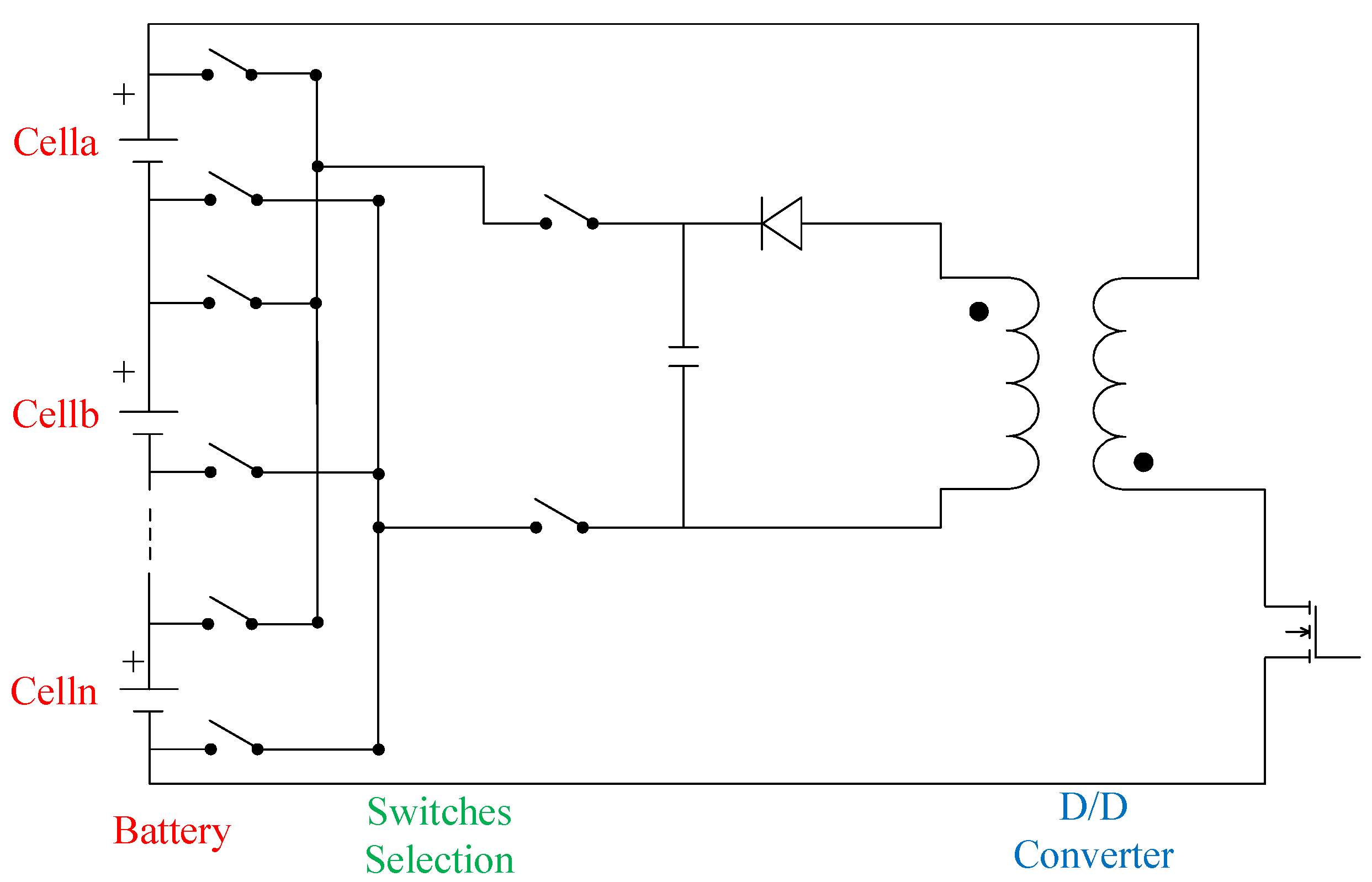
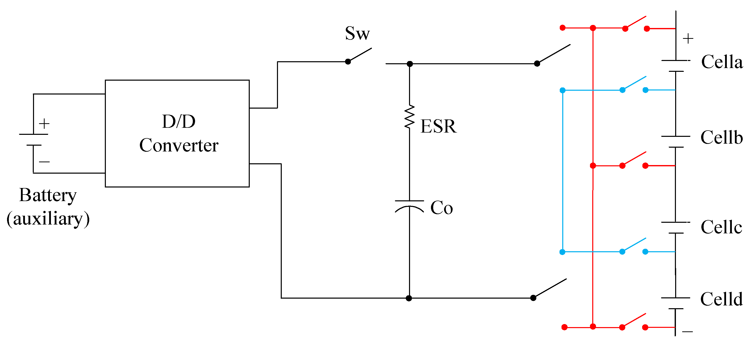
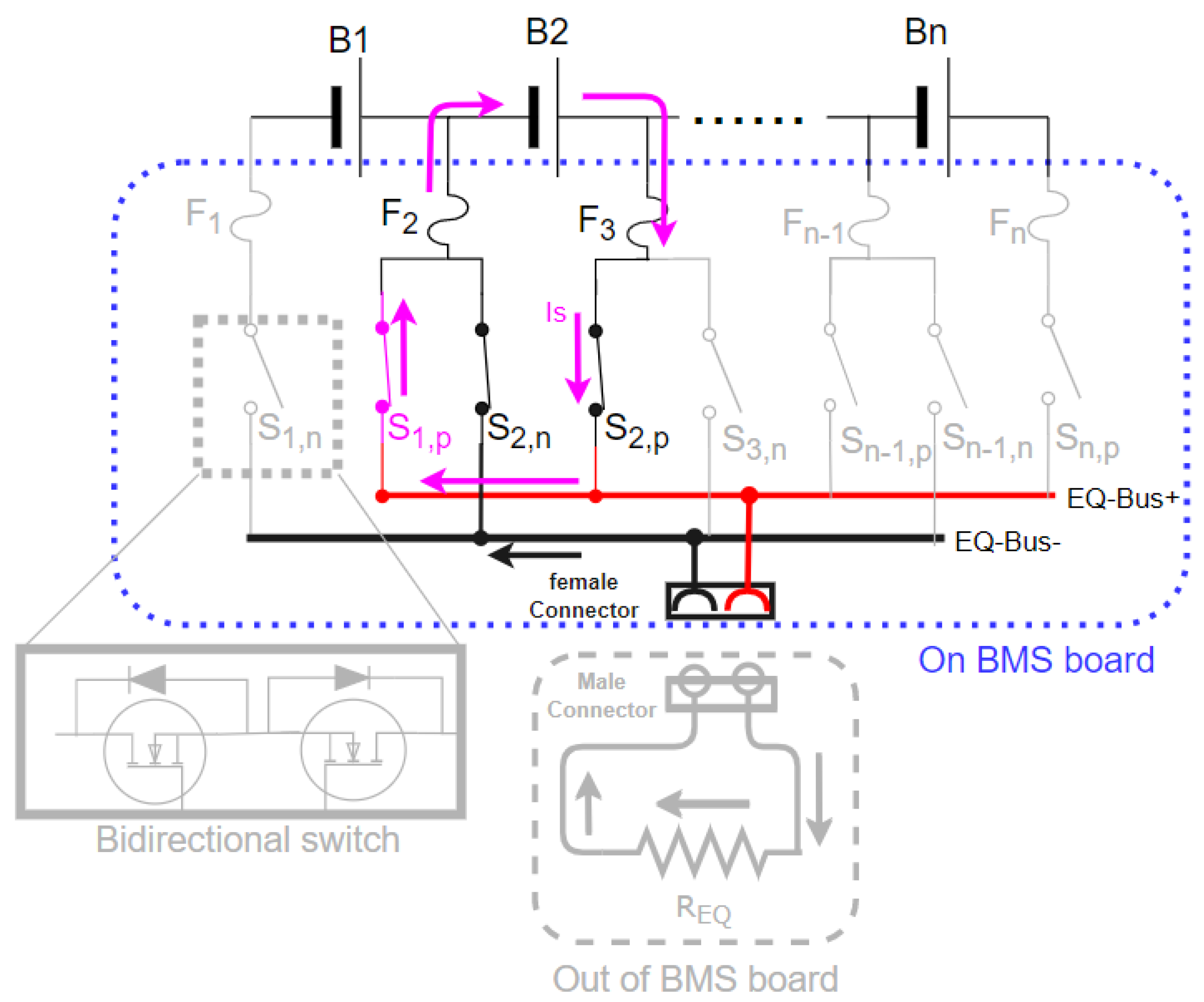
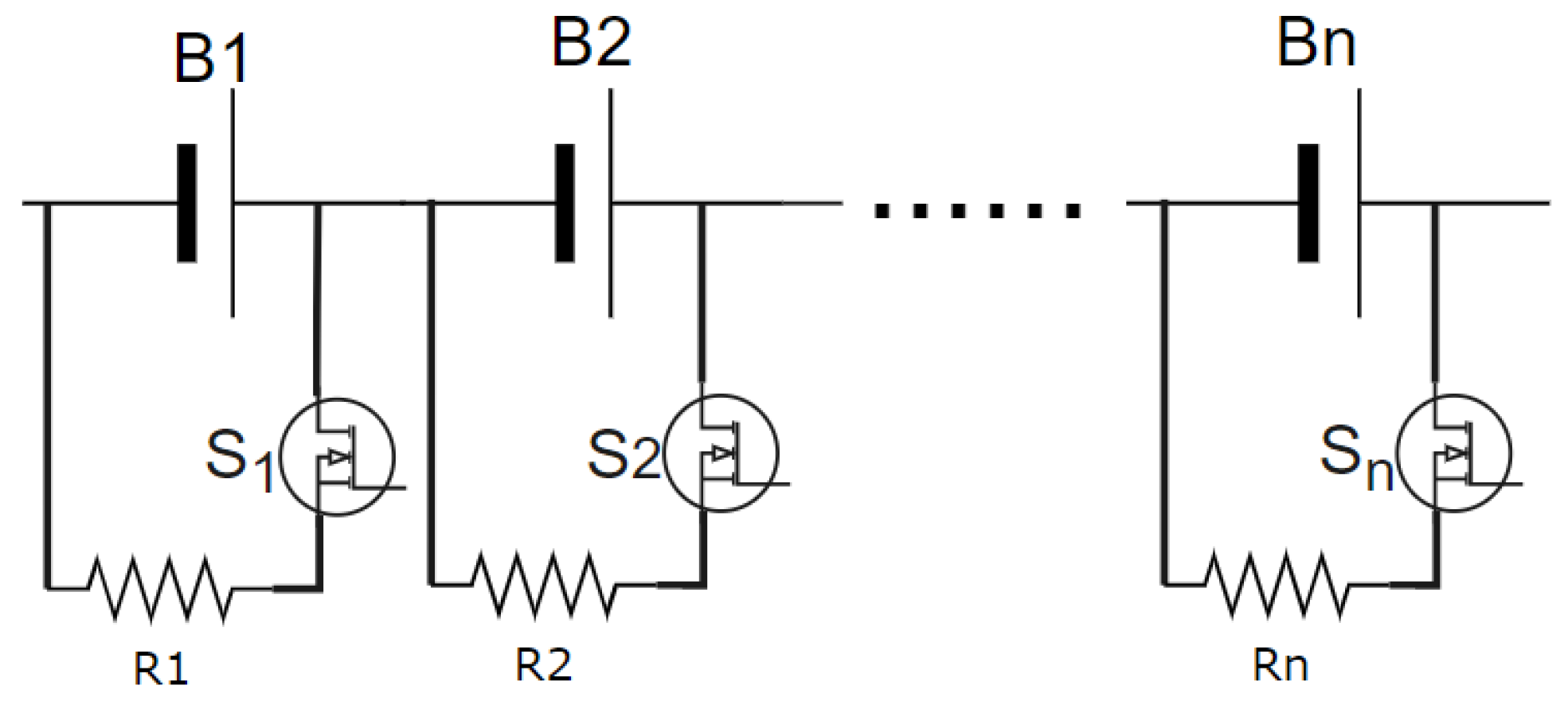
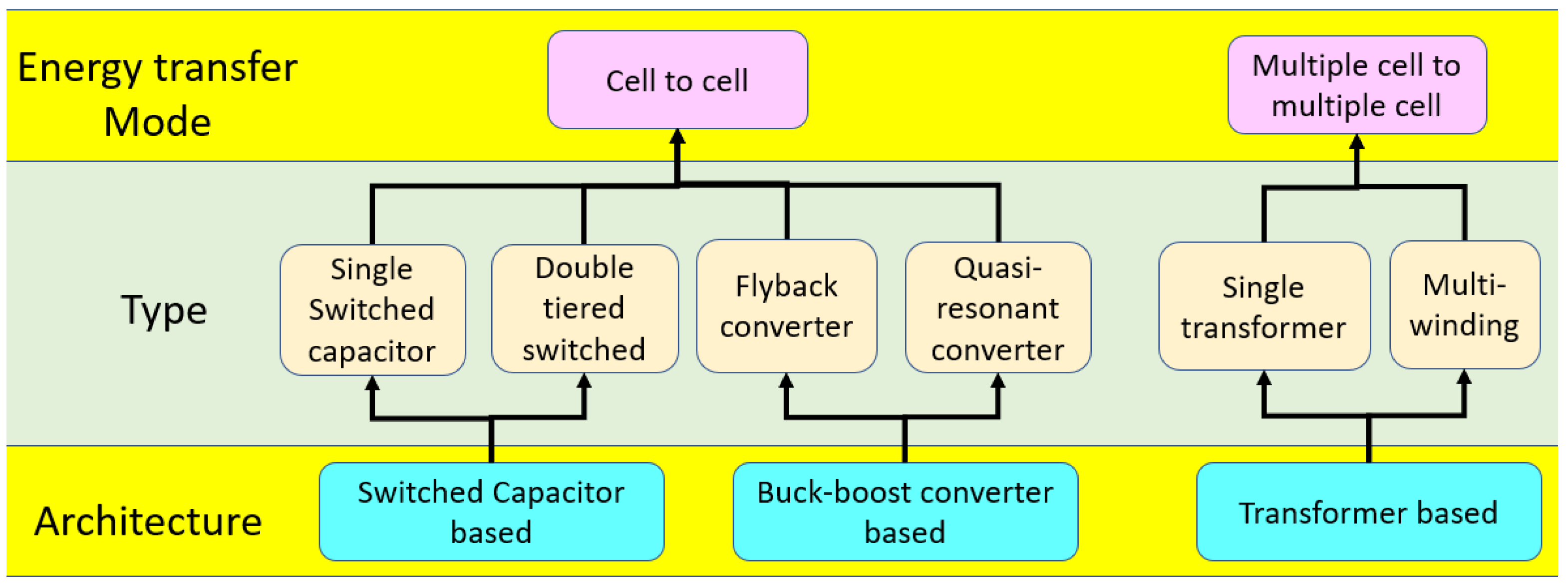
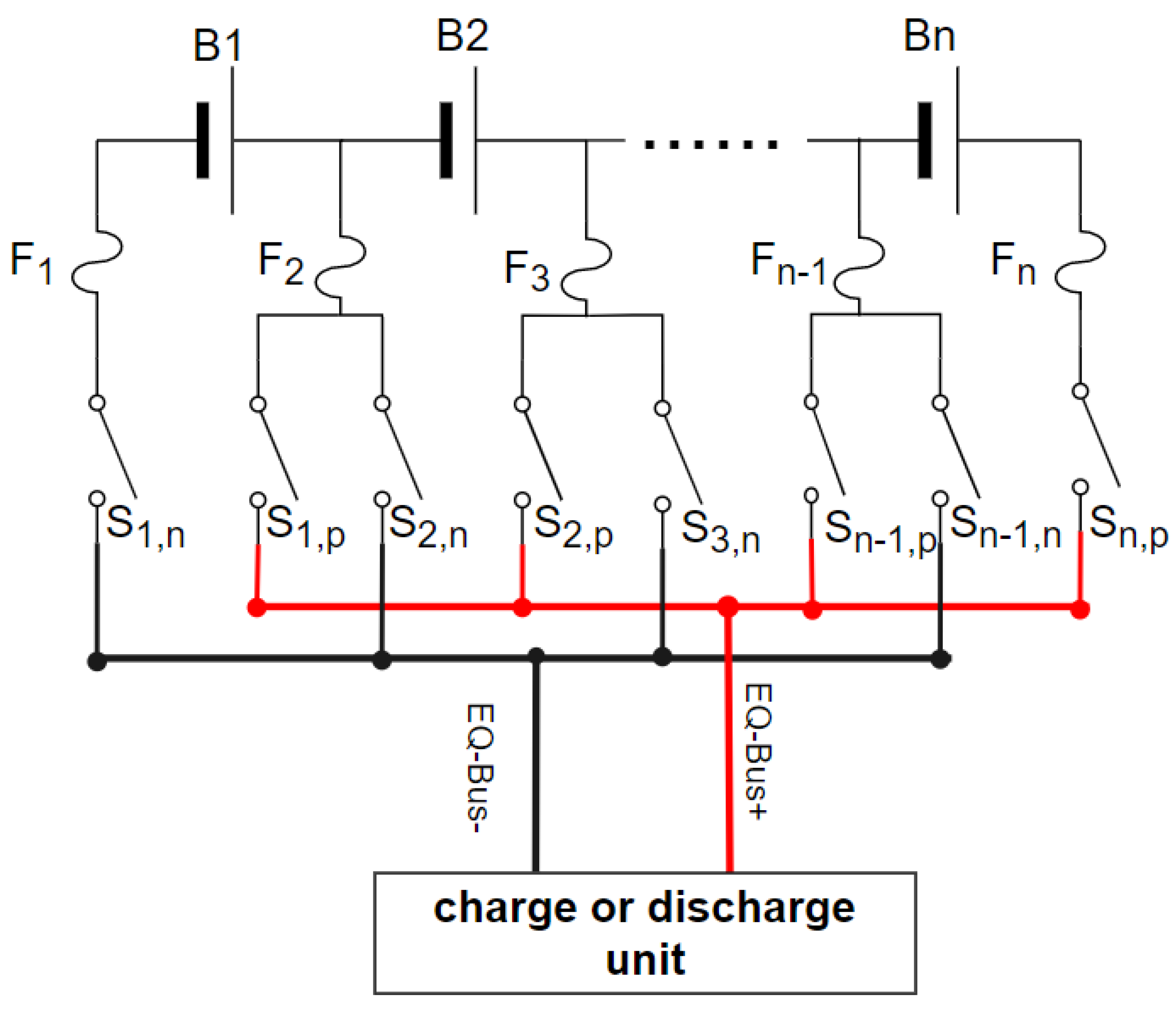
2. Operation Principle of Hybrid Equalizer
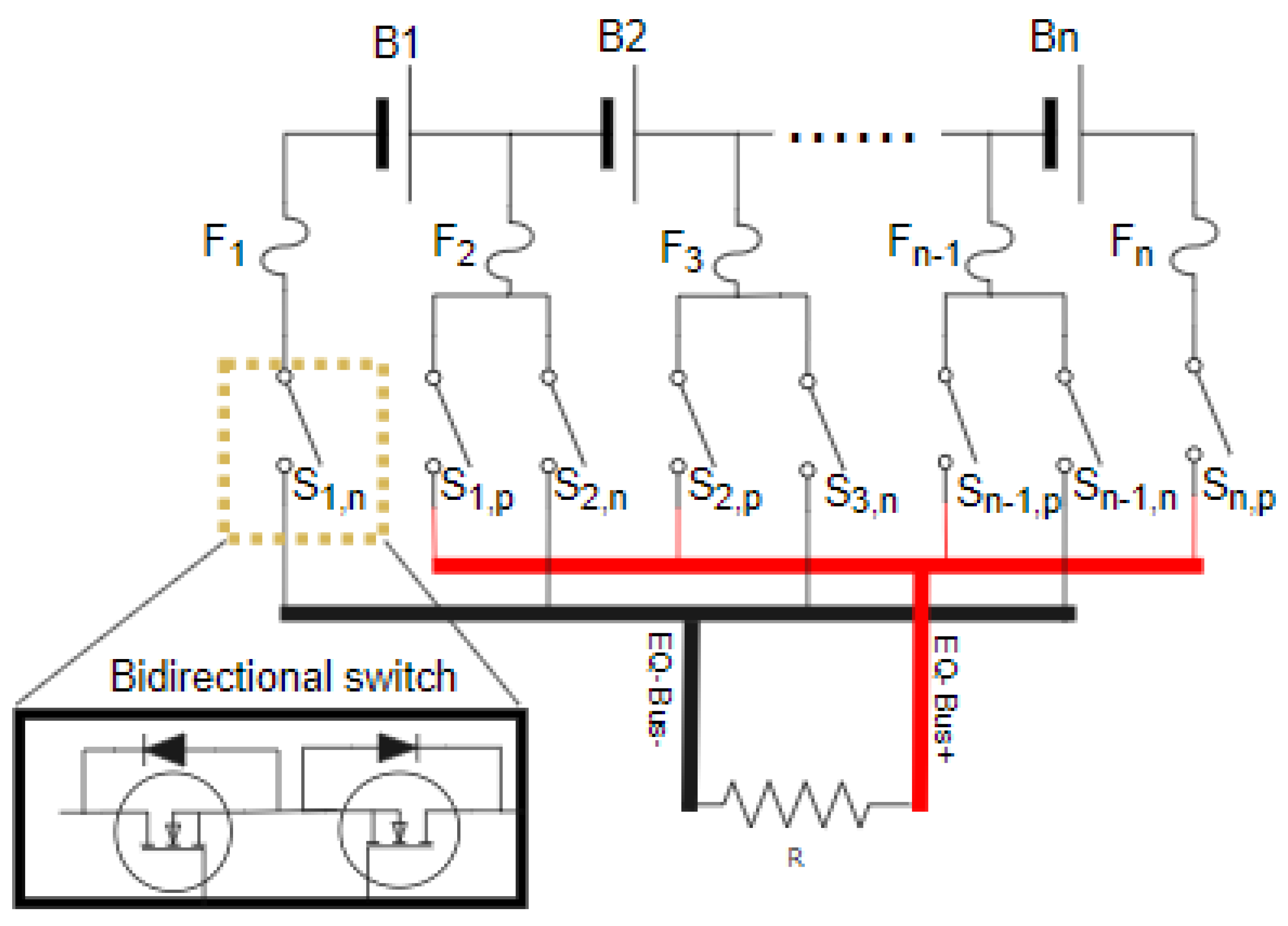
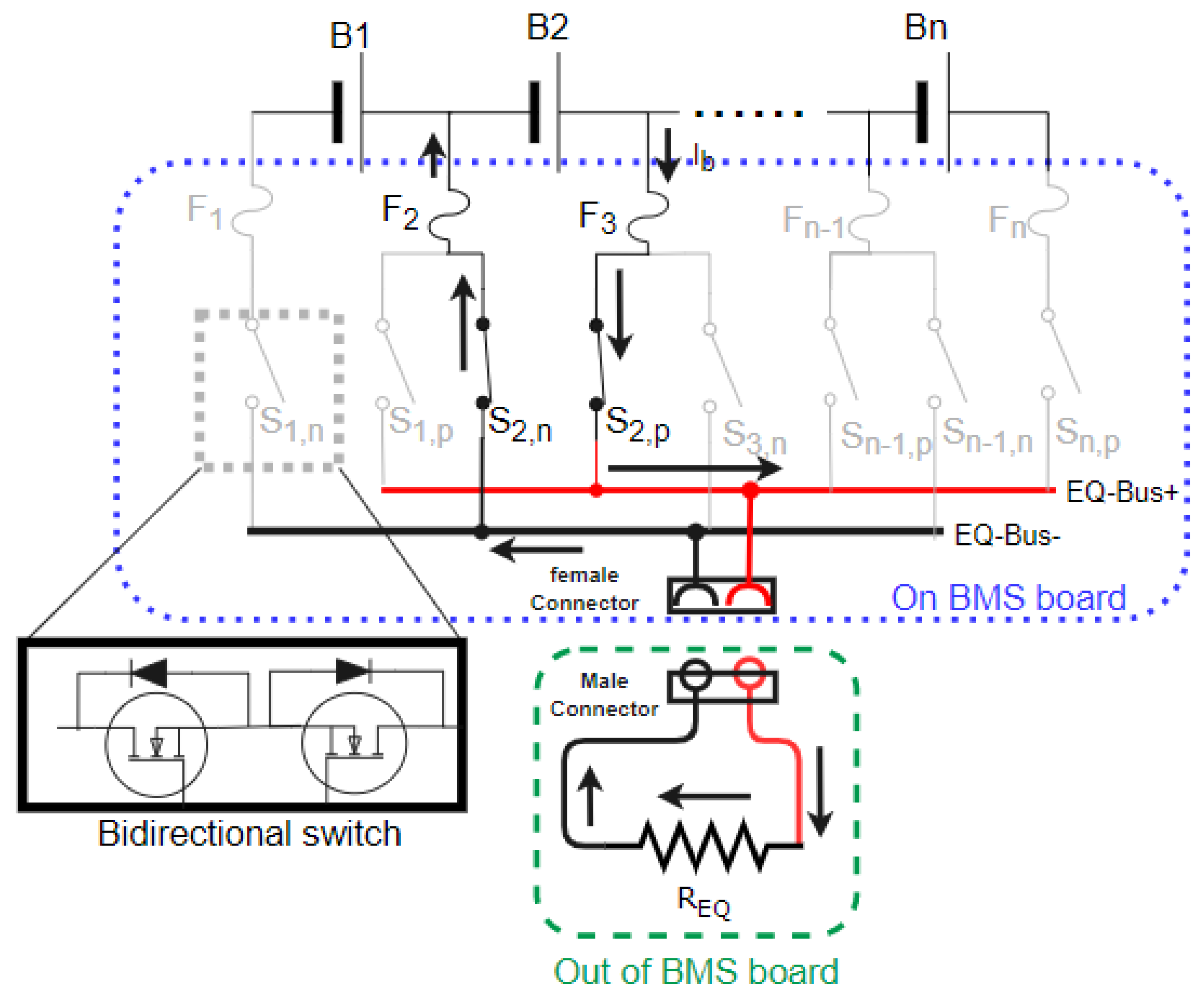
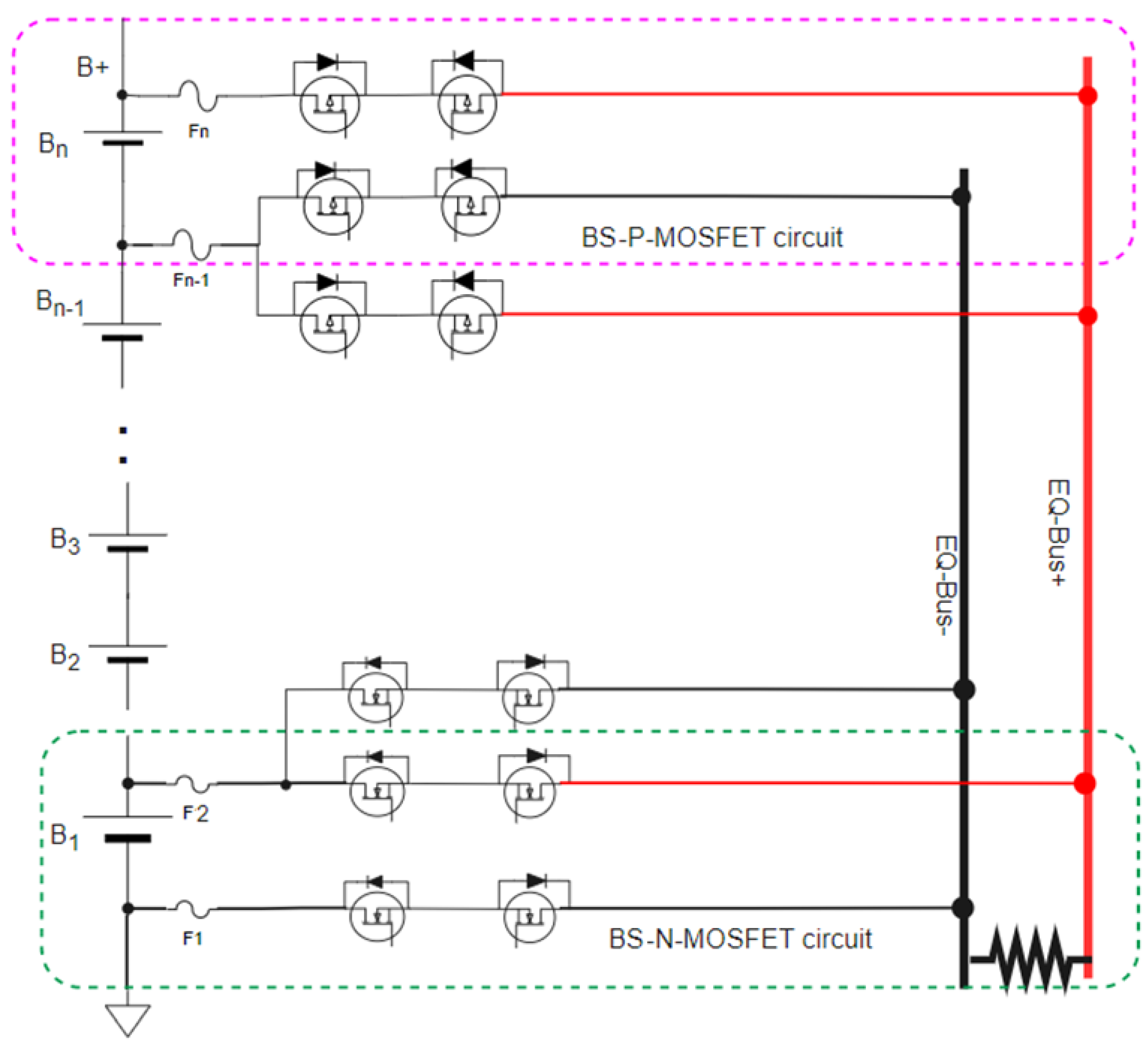
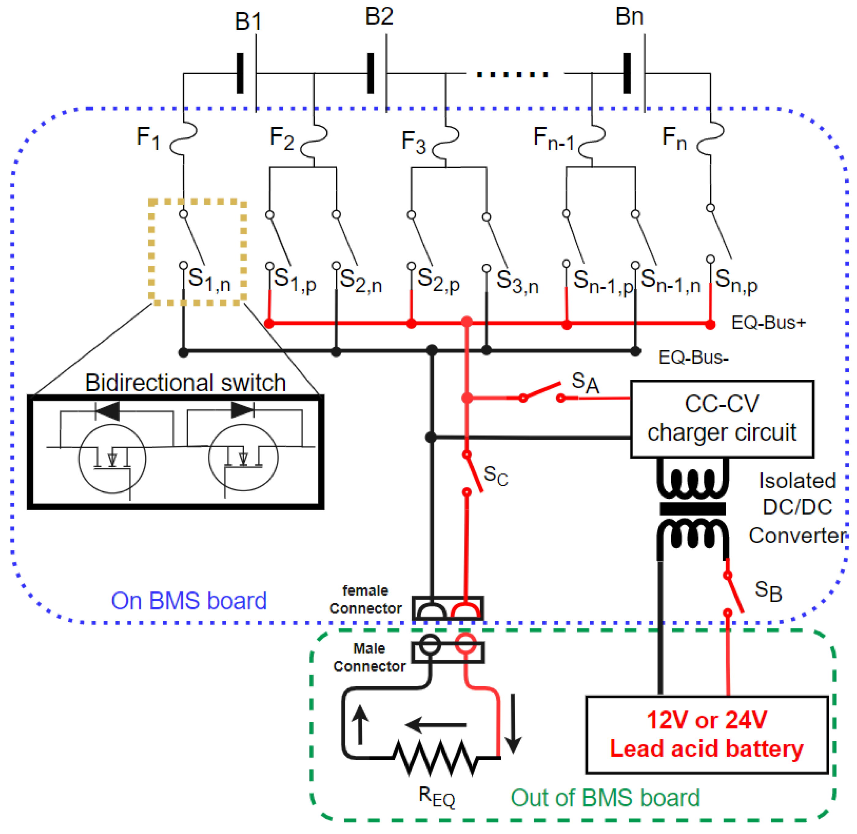
3. Cost-Effective Bidirectional Switch Circuit Design for HEC
3.1. Low-Cost BS-MOSFET Drive Circuit
3.2. BS-P-MOSFET Drive Circuit
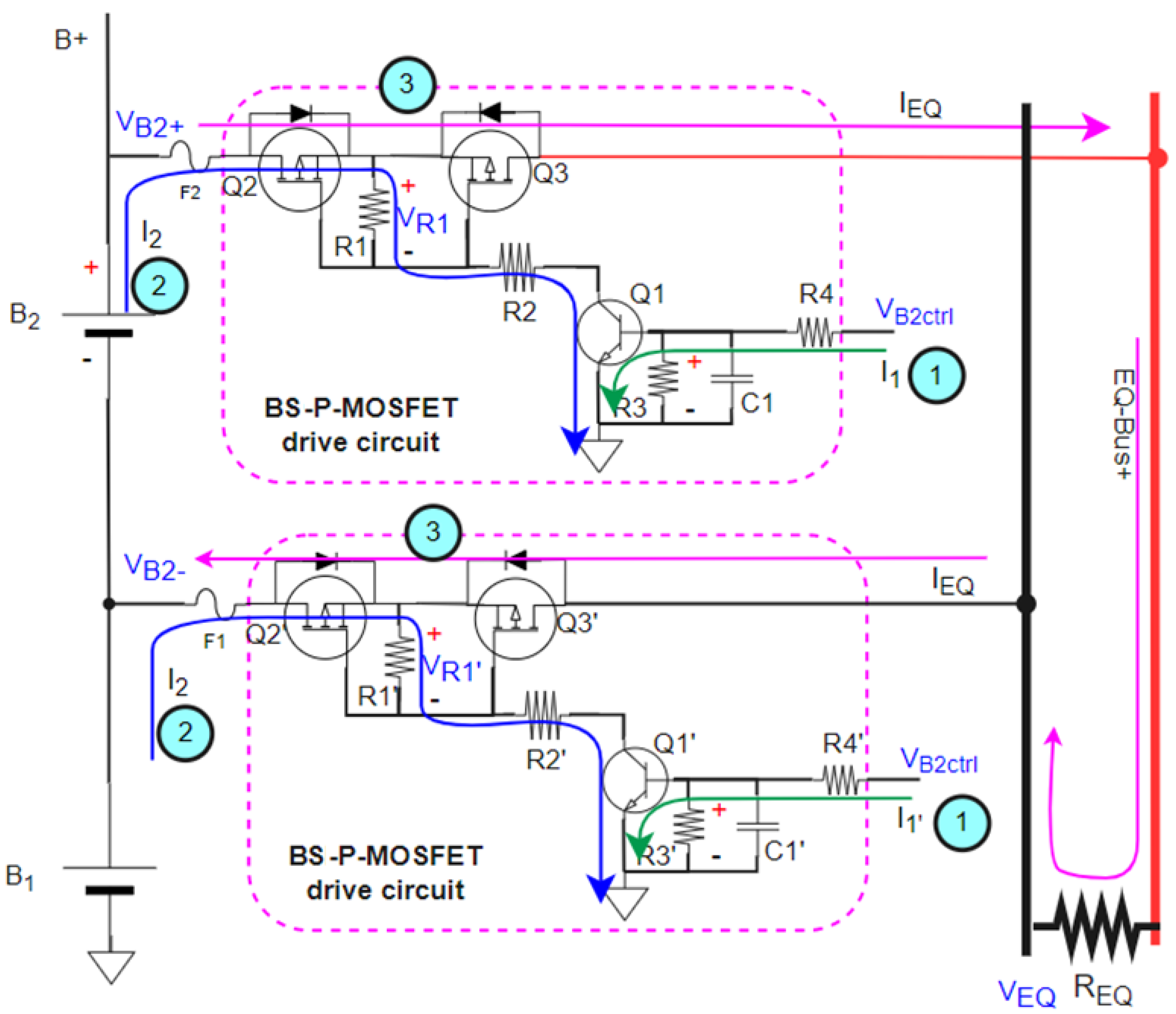
3.2.1. Schematic and Calculation for BS-P-MOSFET Circuit
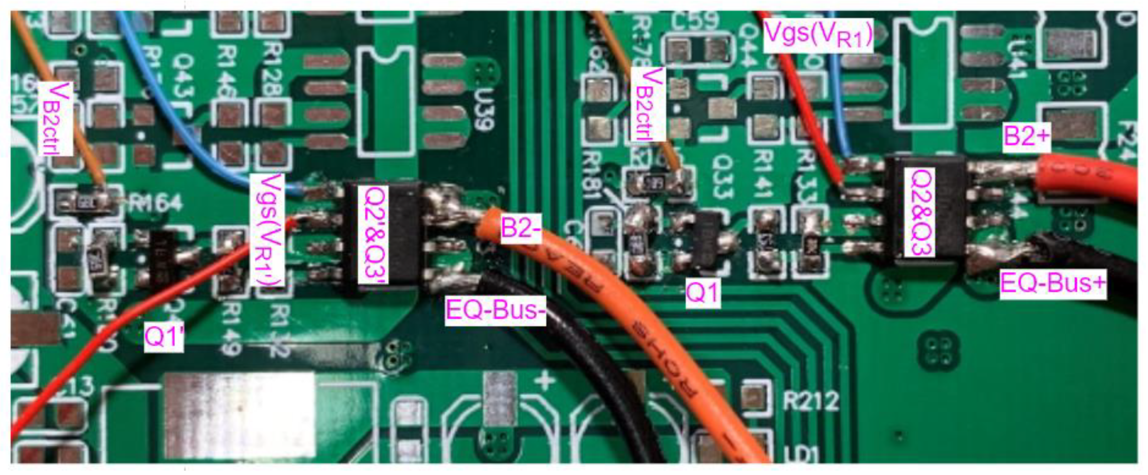
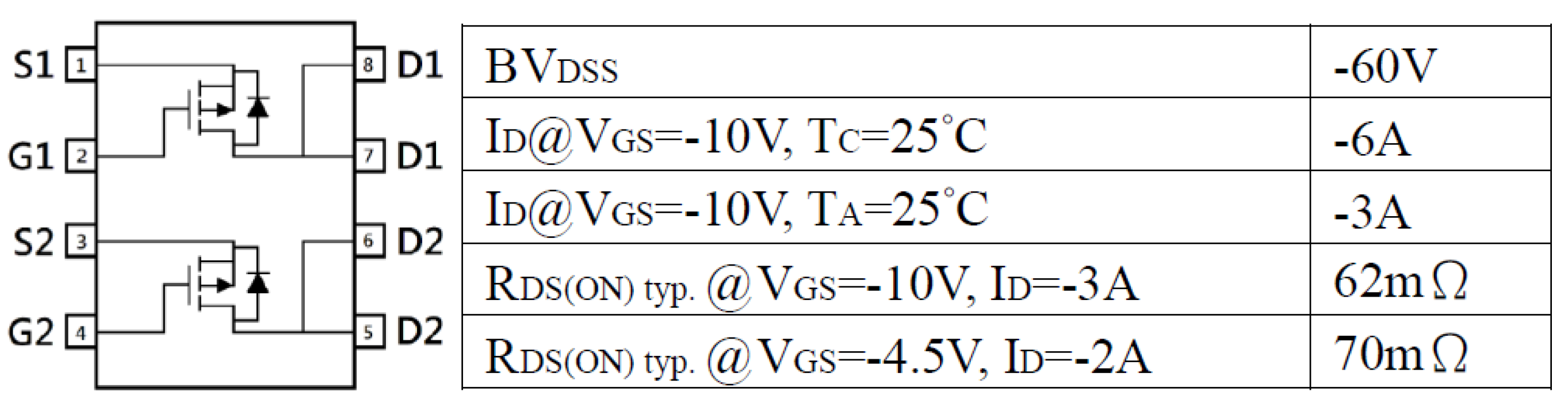
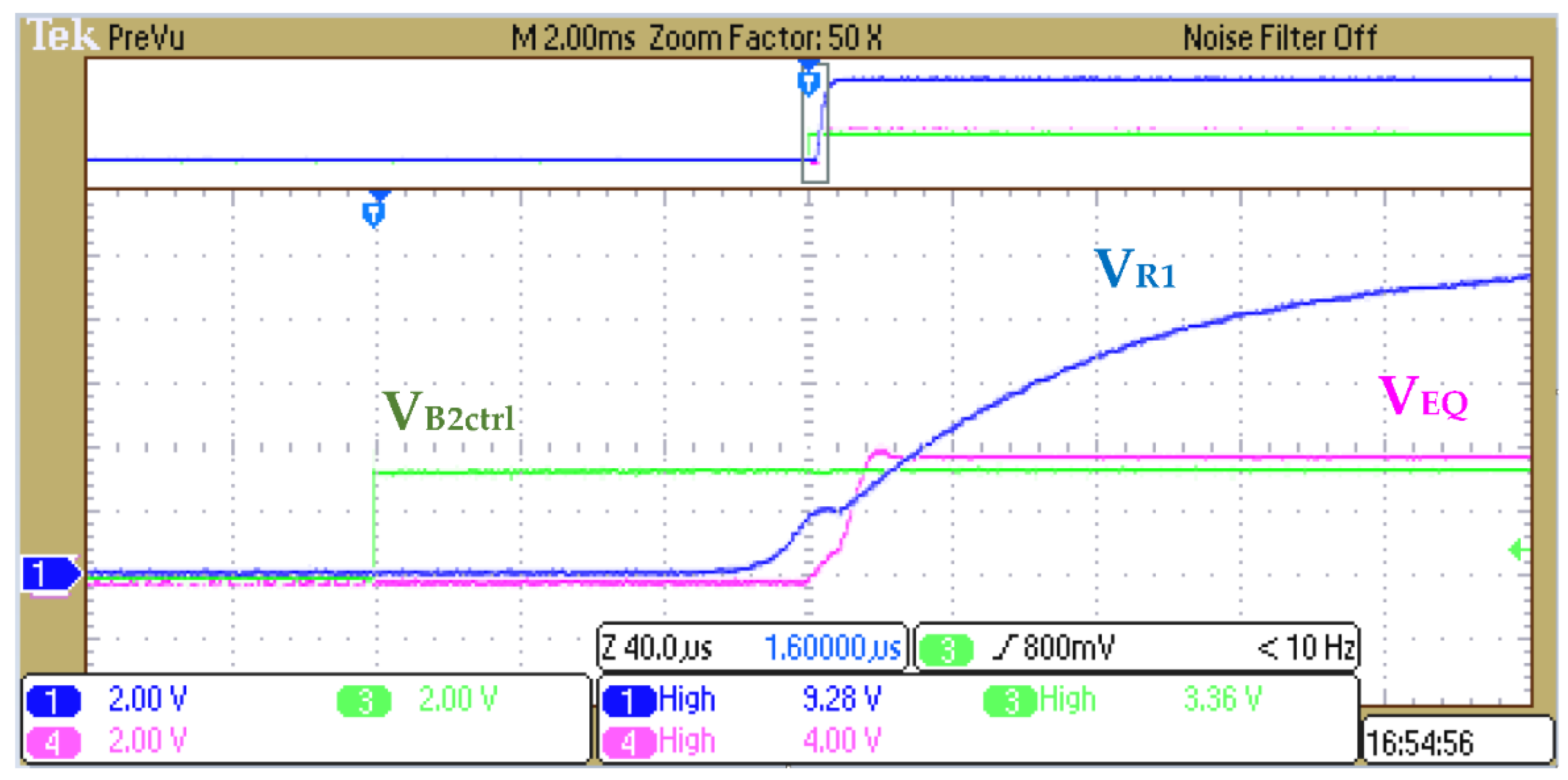
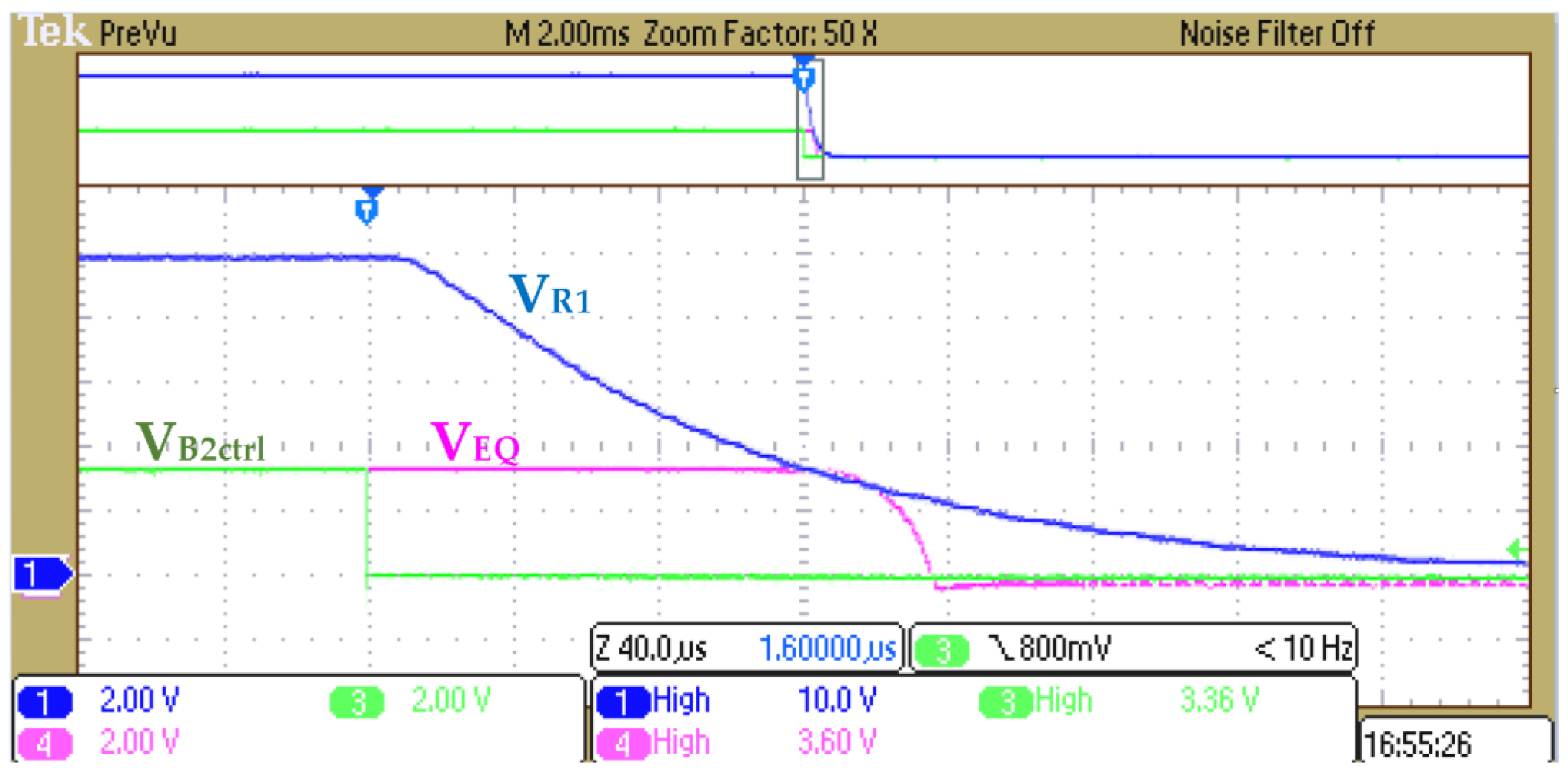
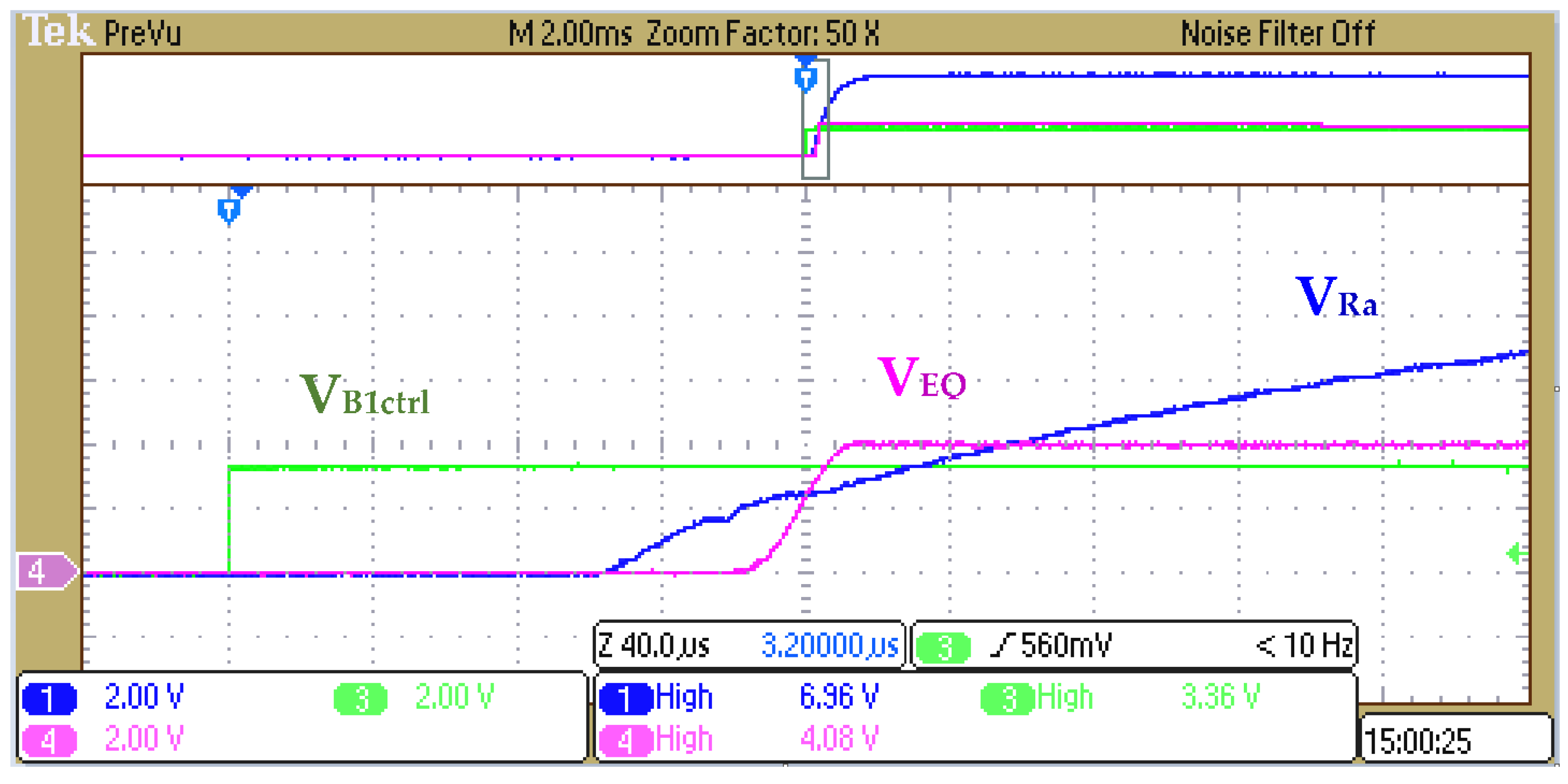
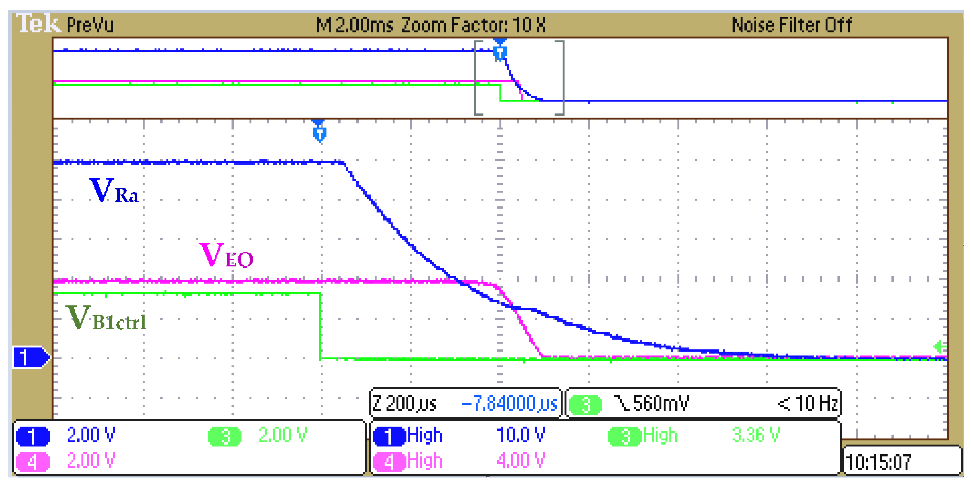
3.2.2. Implementation and Test Results for BS-P-MOSFET Circuit
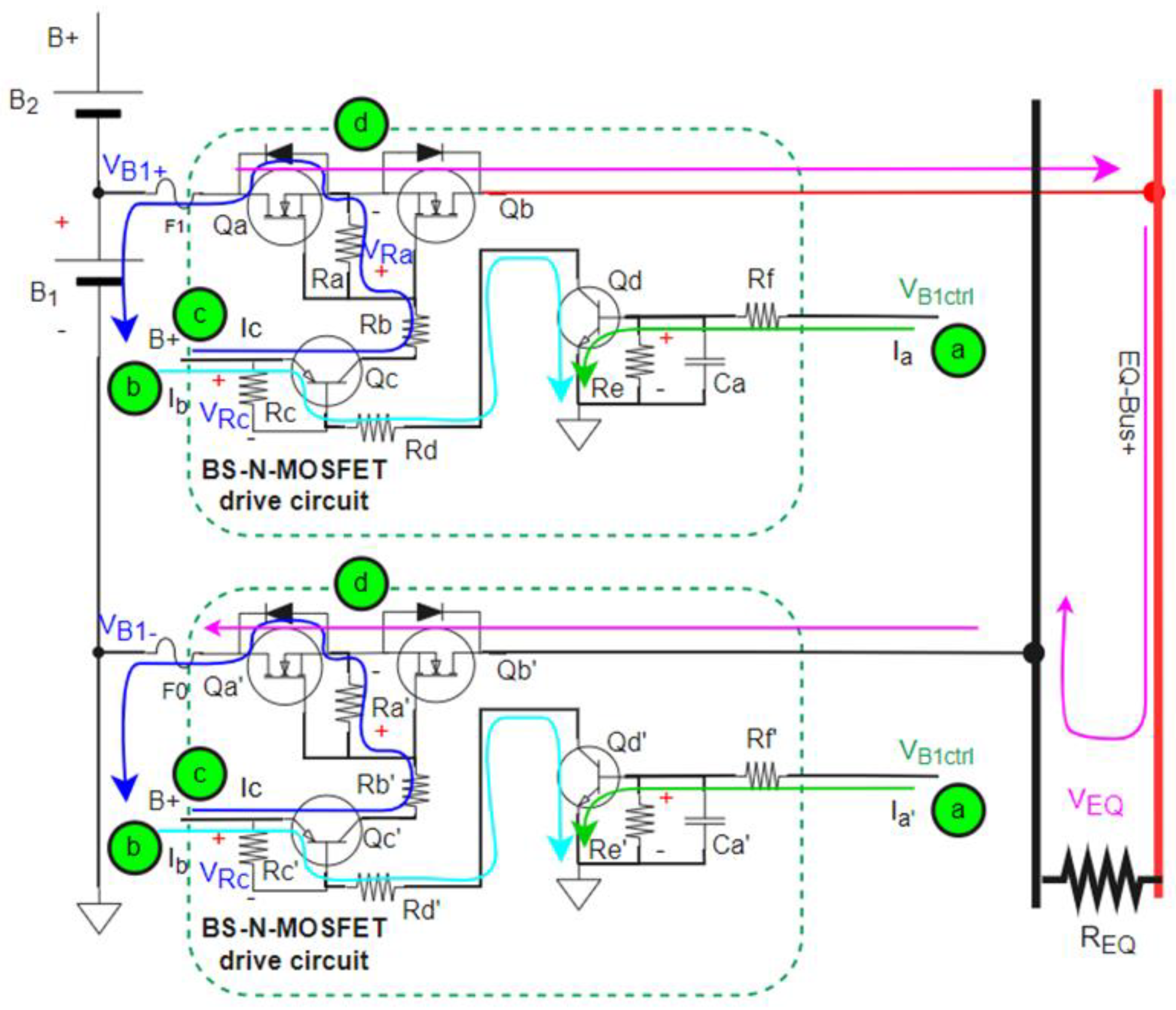
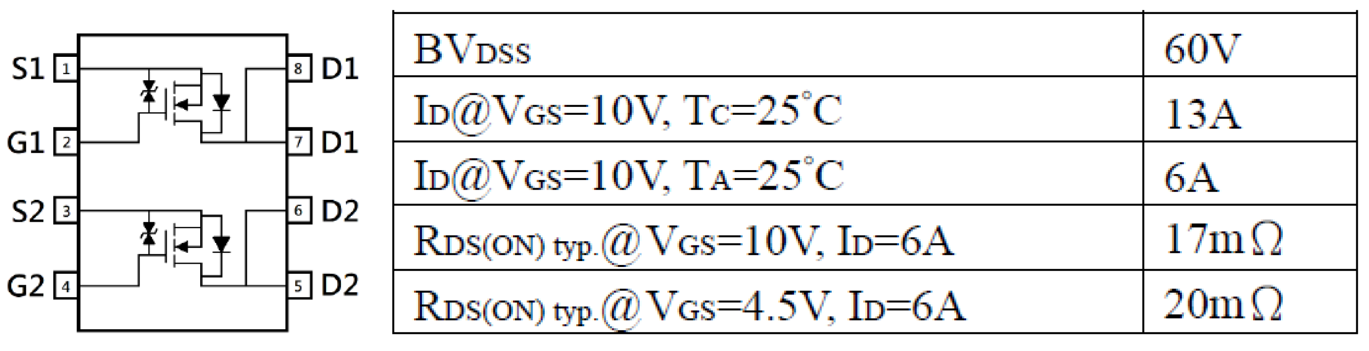
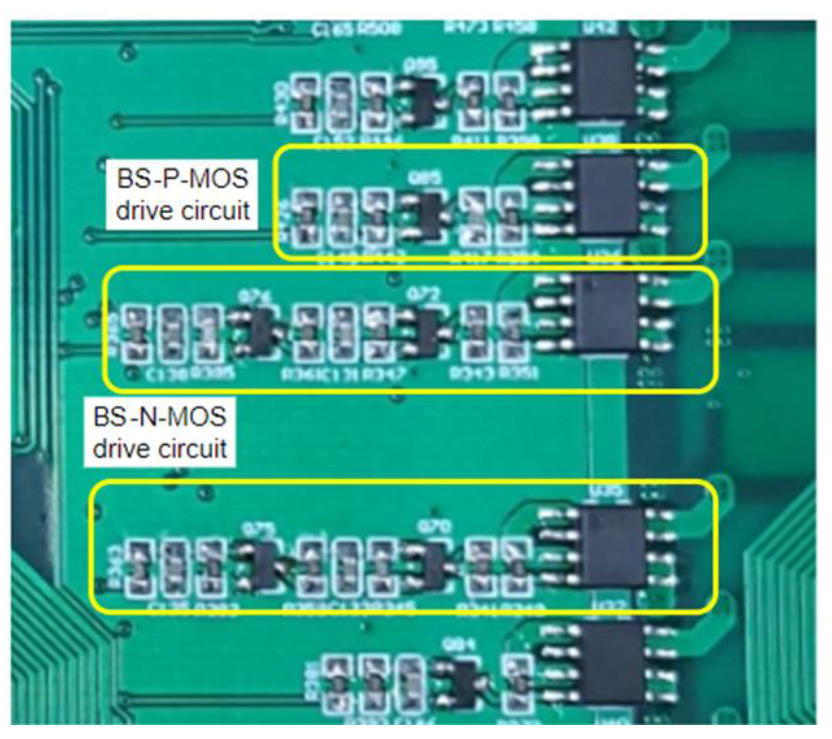
3.3. BS-N-MOSFET Drive Circuit
3.3.1. Schematic and Calculation for BS-N-MOSFET Circuit
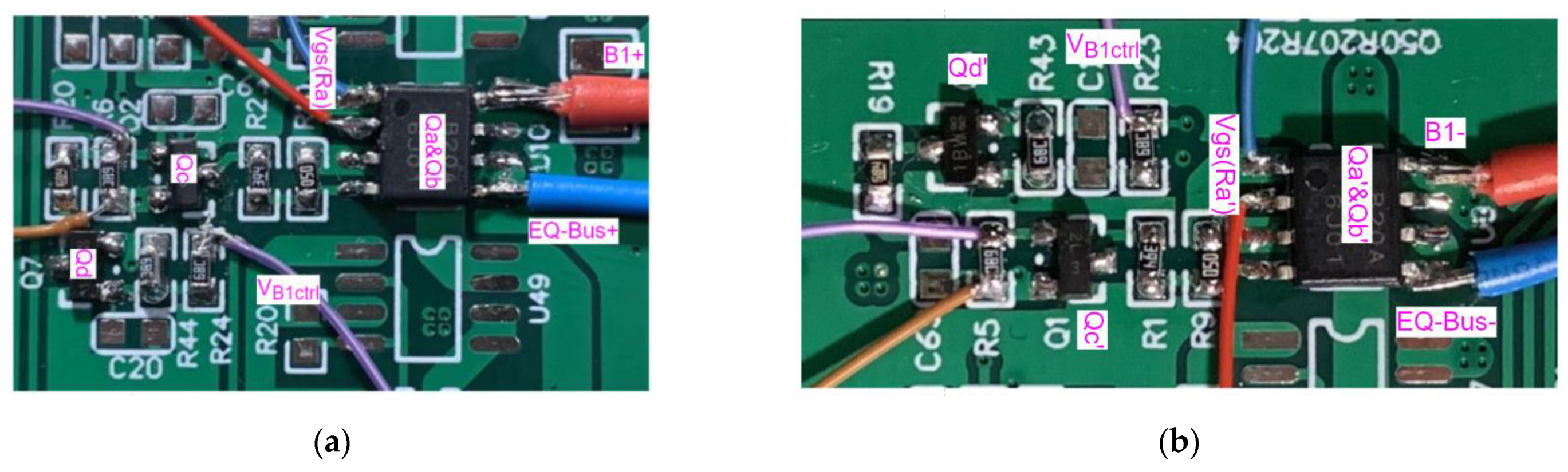
3.3.2. Implementation and Test Results for BS-N-MOSFET Circuit
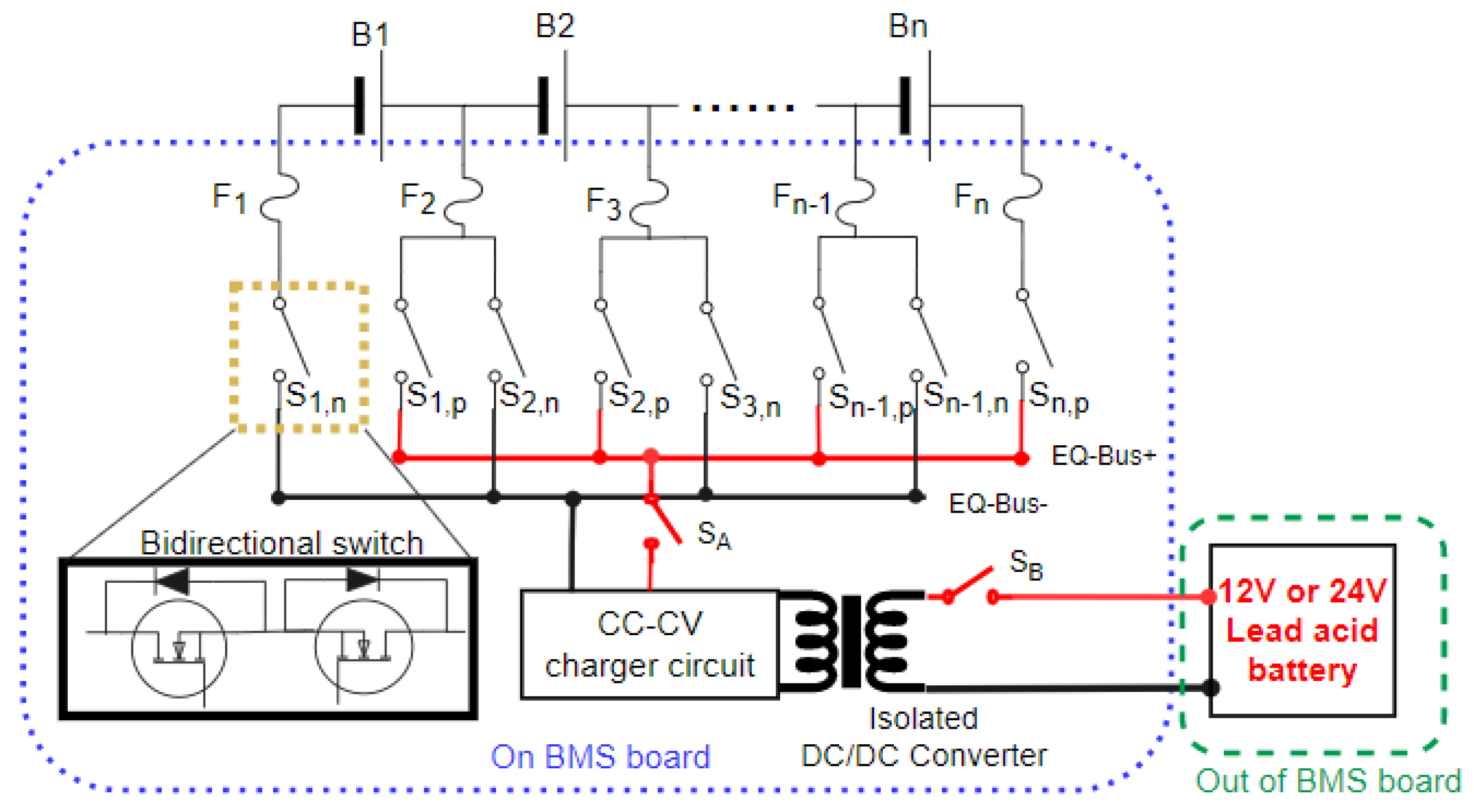
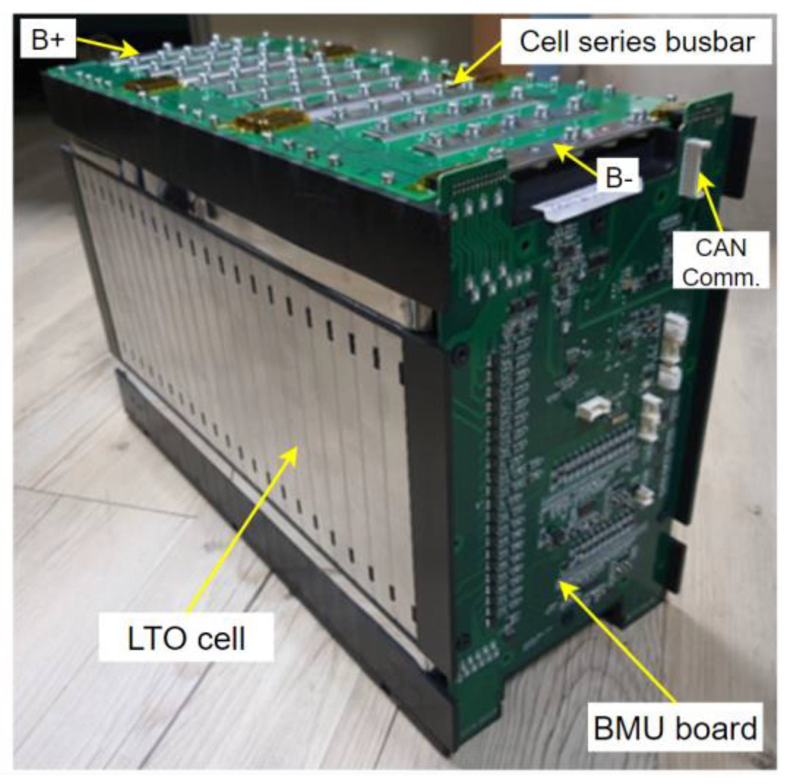
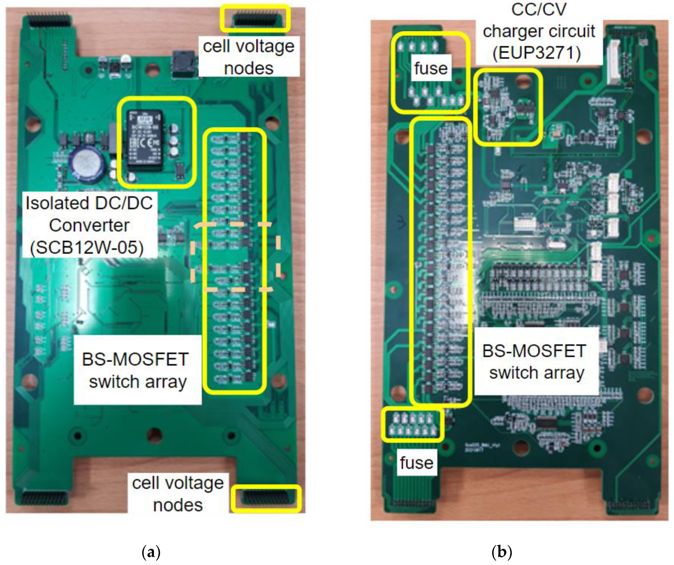
4. Implementation of the A-HEC to the Battery Monitoring Unit of a Battery Pack
5. Conclusions
Author Contributions
Funding
Institutional Review Board Statement
Informed Consent Statement
Conflicts of Interest
Abbreviations
| BMS | Battery management system |
| AFE | Analog front end |
| BMU | Battery monitoring unit |
| EV | Electric vehicle |
| ESS | Energy storage system |
| LIB | Lithium-ion battery |
| EC | Equalizer circuit |
| M-AEC | Modularized equalizer circuit |
| PEC | Passive equalizer circuit |
| AEC | Active equalizer circuit |
| HEC | Hybrid equalizer circuit |
| P-HEC | Passive hybrid equalizer circuit |
| A-HEC | Active hybrid equalizer circuit |
| AP-HEC | Active/passive hybrid equalizer circuit |
| BS | bidirectional switch |
| BS-MOSFET | bidirectional switch with back-to-back MOSFET |
| BS-P-MOSFET | bidirectional switch with back-to-back P-MOSFET |
| BS-N-MOSFET | bidirectional switch with back-to-back N-MOSFET |
References
- Viola, F. Electric Vehicles and Psychology. Sustainability 2021, 13, 719. [Google Scholar] [CrossRef]
- Beaudet, A.; Larouche, F.; Amouzegar, K.; Bouchard, P.; Zaghib, K. Key Challenges and Opportunities for Recycling Electric Vehicle Battery Materials. Sustainability 2020, 12, 5837. [Google Scholar] [CrossRef]
- Gaines, L.; Richa, K.; Spangenberger, J. Key issues for Li-ion battery recycling. MRS Energy Sustain. 2018, 5. [Google Scholar] [CrossRef] [Green Version]
- Pillot, C. The rechargeable battery market and main trends 2018–2030. In Proceedings of the 36th Annual International Battery Seminar & Exhibit, Fort Lauderdale, FL, USA, 25–28 March 2019. [Google Scholar]
- Saqli, K.; Bouchareb, H.; Oudghiri, M.; M’Sirdi, N. Critical Review of Ageing Mechanisms and State of Health Estimation Methods for Battery Performance. In Sustainability in Energy and Buildings; Springer: Berlin/Heidelberg, Germany, 2020; pp. 507–518. [Google Scholar]
- Chou, C.-J.; Jiang, S.-B.; Yeh, T.-L.; Sun, C.-C. Fault-Tolerant Battery Power Network Architecture of Networked Swappable Battery Packs in Parallel. Energies 2021, 14, 2841. [Google Scholar] [CrossRef]
- Carkhuff, B.G.; Demirev, P.A.; Srinivasan, R. Impedance-based battery management system for safety monitoring of lithium-ion batteries. IEEE Trans. Ind. Electron. 2018, 65, 6497–6504. [Google Scholar] [CrossRef]
- Dorn, R.; Schwartz, R.; Steurich, B. Battery management system. In Lithium-Ion Batteries: Basics and Applications; Springer: Berlin/Heidelberg, Germany, 2018; pp. 165–175. [Google Scholar]
- Lelie, M.; Braun, T.; Knips, M.; Nordmann, H.; Ringbeck, F.; Zappen, H.; Sauer, D.U. Battery management system hardware concepts: An overview. Appl. Sci. 2018, 8, 534. [Google Scholar] [CrossRef] [Green Version]
- Li, W.; Cao, D.; Jöst, D.; Ringbeck, F.; Kuipers, M.; Frie, F.; Sauer, D.U. Parameter sensitivity analysis of electrochemical model-based battery management systems for lithium-ion batteries. Appl. Energy 2020, 269, 115104. [Google Scholar] [CrossRef]
- Lipu, M.H.; Hannan, M.; Karim, T.F.; Hussain, A.; Saad, M.H.; Ayob, A.; Miah, M.S.; Mahlia, T. Intelligent algorithms and control strategies for battery management system in electric vehicles: Progress, challenges and future outlook. J. Clean. Prod. 2021, 292, 126044. [Google Scholar] [CrossRef]
- Nizam, M.; Maghfiroh, H.; Rosadi, R.A.; Kusumaputri, K.D. Battery management system design (BMS) for lithium ion batteries. AIP Conf. Proc. 2020, 2217, 30157. [Google Scholar]
- Ren, H.; Zhao, Y.; Chen, S.; Wang, T. Design and implementation of a battery management system with active charge balance based on the SOC and SOH online estimation. Energy 2019, 166, 908–917. [Google Scholar] [CrossRef]
- Tarhan, B.; Yetik, O.; Karakoc, T.H. Hybrid Battery Management System Design for Electric Aircraft. Energy 2021, 234, 121227. [Google Scholar] [CrossRef]
- Turkmanović, H.; Popović, I. A systematic approach for designing battery management system for embedded applications. In Proceedings of the 2021 Zooming Innovation in Consumer Technologies Conference (ZINC), Novi Sad, Serbia, 26–27 May 2021; pp. 85–90. [Google Scholar]
- Wang, X.; Wei, X.; Zhu, J.; Dai, H.; Zheng, Y.; Xu, X.; Chen, Q. A review of modeling, acquisition, and application of lithium-ion battery impedance for onboard battery management. ETransportation 2021, 7, 100093. [Google Scholar] [CrossRef]
- Wang, Y.; Tian, J.; Sun, Z.; Wang, L.; Xu, R.; Li, M.; Chen, Z. A comprehensive review of battery modeling and state estimation approaches for advanced battery management systems. Renew. Sustain. Energy Rev. 2020, 131, 110015. [Google Scholar] [CrossRef]
- Pernaci, C.; Muscato, G.; Scandurra, A. Test of Automotive Battery Management System Control Strategies on Hardware-in-the-Loop Systems: A Low-Voltage Approach. SAE Int. J. Electrified Veh. 2021, 10, 123. [Google Scholar] [CrossRef]
- Lai, X.; Huang, Y.; Gu, H.; Han, X.; Feng, X.; Dai, H.; Zheng, Y.; Ouyang, M. Remaining discharge energy estimation for lithium-ion batteries based on future load prediction considering temperature and ageing effects. Energy 2022, 238, 121754. [Google Scholar] [CrossRef]
- Bui, T.M.; Niri, M.F.; Worwood, D.; Dinh, T.Q.; Marco, J. An Advanced Hardware-in-the-Loop Battery Simulation Platform for the Experimental Testing of Battery Management System. In Proceedings of the 2019 23rd International Conference on Mechatronics Technology (ICMT), Salerno, Italy, 23–26 October 2019; pp. 1–6. [Google Scholar]
- Khalid, A.; Stevenson, A.; Sarwat, A.I. Performance Analysis of Commercial Passive Balancing Battery Management System Operation Using a Hardware-in-the-Loop Testbed. Energies 2021, 14, 8037. [Google Scholar] [CrossRef]
- Habib, A.A.; Hasan, M.K.; Mahmud, M.; Motakabber, S.; Ibrahimya, M.I.; Islam, S. A review: Energy storage system and balancing circuits for electric vehicle application. IET Power Electron. 2021, 14, 1–13. [Google Scholar] [CrossRef]
- Tang, X.; Zou, C.; Wik, T.; Yao, K.; Xia, Y.; Wang, Y.; Yang, D.; Gao, F. Run-to-run control for active balancing of lithium iron phosphate battery packs. IEEE Trans. Power Electron. 2019, 35, 1499–1512. [Google Scholar] [CrossRef] [Green Version]
- Ouyang, Q.; Chen, J.; Zheng, J.; Fang, H. Optimal cell-to-cell balancing topology design for serially connected lithium-ion battery packs. IEEE Trans. Sustain. Energy 2017, 9, 350–360. [Google Scholar] [CrossRef]
- Ouyang, Q.; Chen, J.; Xu, C.; Su, H. Cell balancing control for serially connected lithium-ion batteries. In Proceedings of the 2016 American Control Conference (ACC), Boston, MA, USA, 6–8 July 2016; pp. 3095–3100. [Google Scholar]
- Feng, F.; Hu, X.; Liu, J.; Lin, X.; Liu, B. A review of equalization strategies for series battery packs: Variables, objectives, and algorithms. Renew. Sustain. Energy Rev. 2019, 116, 109464. [Google Scholar] [CrossRef]
- Diao, W.; Xue, N.; Bhattacharjee, V.; Jiang, J.; Karabasoglu, O.; Pecht, M. Active battery cell equalization based on residual available energy maximization. Appl. Energy 2018, 210, 690–698. [Google Scholar] [CrossRef]
- Hua, Y.; Zhou, S.; Cui, H.; Liu, X.; Zhang, C.; Xu, X.; Ling, H.; Yang, S. A comprehensive review on inconsistency and equalization technology of lithium-ion battery for electric vehicles. Int. J. Energy Res. 2020, 44, 11059–11087. [Google Scholar] [CrossRef]
- Lee, S.-W.; Lee, K.-M.; Choi, Y.-G.; Kang, B. Modularized design of active charge equalizer for Li-ion battery pack. IEEE Trans. Ind. Electron. 2018, 65, 8697–8706. [Google Scholar] [CrossRef]
- Das, U.K.; Shrivastava, P.; Tey, K.S.; Idris, M.Y.I.B.; Mekhilef, S.; Jamei, E.; Seyedmahmoudian, M.; Stojcevski, A. Advancement of lithium-ion battery cells voltage equalization techniques: A review. Renew. Sustain. Energy Rev. 2020, 134, 110227. [Google Scholar] [CrossRef]
- Hsieh, Y.C.; Yu, L.R.; Yang, M.F. A charge equalization scheme for battery string with charging current allocation. Int. J. Circuit Theory Appl. 2021, 49, 2935–2945. [Google Scholar] [CrossRef]
- Gallardo-Lozano, J.; Romero-Cadaval, E.; Milanes-Montero, M.I.; Guerrero-Martinez, M.A. Battery equalization active methods. J. Power Source 2014, 246, 934–949. [Google Scholar] [CrossRef]
- Carter, J.; Fan, Z.; Cao, J. Cell equalisation circuits: A review. J. Power Source 2020, 448, 227489. [Google Scholar] [CrossRef]
- Daowd, M.; Antoine, M.; Omar, N.; Lataire, P.; Van Den Bossche, P.; Van Mierlo, J. Battery management system—Balancing modularization based on a single switched capacitor and bi-directional DC/DC converter with the auxiliary battery. Energies 2014, 7, 2897–2937. [Google Scholar] [CrossRef] [Green Version]
- Daowd, M.; Antoine, M.; Omar, N.; Van den Bossche, P.; Van Mierlo, J. Single switched capacitor battery balancing system enhancements. Energies 2013, 6, 2149–2174. [Google Scholar] [CrossRef] [Green Version]
- Turksoy, A.; Teke, A.; Alkaya, A. A comprehensive overview of the dc-dc converter-based battery charge balancing methods in electric vehicles. Renew. Sustain. Energy Rev. 2020, 133, 110274. [Google Scholar] [CrossRef]
- Omariba, Z.B.; Zhang, L.; Sun, D. Review of battery cell balancing methodologies for optimizing battery pack performance in electric vehicles. IEEE Access 2019, 7, 129335–129352. [Google Scholar] [CrossRef]
- Koseoglou, M.; Tsioumas, E.; Jabbour, N.; Mademlis, C. Highly effective cell equalization in a lithium-ion battery management system. IEEE Trans. Power Electron. 2019, 35, 2088–2099. [Google Scholar] [CrossRef]
- Scott, K.; Nork, S. Passive Balancing Allows All Cells to Appear to Have the Same Capacity. Available online: https://www.analog.com/en/technical-articles/passive-battery-cell-balancing.html (accessed on 13 February 2022).
- Scott, K.; Nork, S. Active Battery Cell Balancing. Available online: https://www.analog.com/en/technical-articles/active-battery-cell-balancing.html (accessed on 13 February 2022).


| Item | PEC (Conventional) | P-HEC (Proposed) |
|---|---|---|
| Topology | 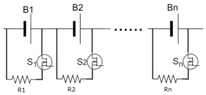 |  |
| Limitation | --- | Pack voltage > 8 V |
| Architecture | Switch + resistor | Cell selector + Discharge unit |
| MOSFET numbers/cost | N (Number of series cell) ~0.15 USD/MOSFET | (N + 1) × 2(Dual package) ~0.25 USD/Dual MOSFET |
| Channel cost | ~0.2 USD/channel | ~0.35 USD/channel |
| Max. ON channel | ≤2 (Limited by heat) | 1 |
| Fail-safe | --- | Yes (fuse) |
| Discharge unit | Power resistor × N (Typical: 33 Ω) | Power resistor × 1 (Typical:2 Ω), Fan or heater |
| Max. current | ~0.127 A@4.2 V | ~2.1 A@4.2 V |
| Waste heat | 0.3–0.5 W/channel | 4.5~8 W |
| Power cost | ~0.4 USD/W (0.2 USD/0.5 W) | ~0.04 USD/W (0.35 USD/8 W) |
| Location | On BMS board | Out of BMS board |
| Occupied area | 1× (Including N resistors) | 1.5–2× (Only fuse and switch arrays are placed on BMS) |
| Item | AEC (Commercial LT8584) | A-HEC (Proposed) |
|---|---|---|
| Topology |  |  |
| Architecture | DC/DC converter | Cell selector + isolated charger |
| Channel cost | N × 6 USD LT8584 (~4) +Transformer (~2) Transformer: COILCRAFT NA5743-AL | (N × 0.25 × 2) + 15 USD Switch array(N × 0.25 × 2 paths) +Charger (~3) +Isolated DC/DC converter (~12) Iso. DC/DC: MEANWELL SCW12B-05 |
| Max. ON channel | Multi-channel | 1 channel |
| Fail-safe | --- | Yes (fuse) |
| Max. current | N × 2.5 A | ~2.1 A@4.2 V |
| Voltage Node | Balancing Charge Current (mA) | Voltage Node | Balancing Charge Current (mA) |
|---|---|---|---|
| B1+ | 2265 | B12+ | 2265 |
| B2+ | 2270 | B13+ | 2270 |
| B3+ | 2255 | B14+ | 2265 |
| B4+ | 2260 | B15+ | 2220 |
| B5+ | 2265 | B16+ | 2270 |
| B6+ | 2265 | B17+ | 2245 |
| B7+ | 2270 | B18+ | 2270 |
| B8+ | 2270 | B19+ | 1960 |
| B9+ | 2265 | B20+ | 1955 |
| B10+ | 2260 | B21+ | 1975 |
| B11+ | 2260 | B22+ | 2260 |
Publisher’s Note: MDPI stays neutral with regard to jurisdictional claims in published maps and institutional affiliations. |
© 2022 by the authors. Licensee MDPI, Basel, Switzerland. This article is an open access article distributed under the terms and conditions of the Creative Commons Attribution (CC BY) license (https://creativecommons.org/licenses/by/4.0/).
Share and Cite
Sun, C.-C.; Chou, C.-H.; Lin, Y.-L.; Huang, Y.-H. A Cost-Effective Passive/Active Hybrid Equalizer Circuit Design. Energies 2022, 15, 2000. https://doi.org/10.3390/en15062000
Sun C-C, Chou C-H, Lin Y-L, Huang Y-H. A Cost-Effective Passive/Active Hybrid Equalizer Circuit Design. Energies. 2022; 15(6):2000. https://doi.org/10.3390/en15062000
Chicago/Turabian StyleSun, Chein-Chung, Chun-Hung Chou, Yu-Liang Lin, and Yu-Hua Huang. 2022. "A Cost-Effective Passive/Active Hybrid Equalizer Circuit Design" Energies 15, no. 6: 2000. https://doi.org/10.3390/en15062000
APA StyleSun, C.-C., Chou, C.-H., Lin, Y.-L., & Huang, Y.-H. (2022). A Cost-Effective Passive/Active Hybrid Equalizer Circuit Design. Energies, 15(6), 2000. https://doi.org/10.3390/en15062000