Article

A New Optimal Thermal-Based Adaptive Frequency Control for Bidirectional DC–DC Converter with Full-Range ZVS

1
School of Traffic and Transportation Engineering, Central South University, Changsha 410017, China
2
School of Automation, Central South University, Changsha 410017, China
*
Author to whom correspondence should be addressed.
Energies 2022, 15(21), 8250; https://doi.org/10.3390/en15218250
Submission received: 22 September 2022 / Revised: 31 October 2022 / Accepted: 2 November 2022 / Published: 4 November 2022

Abstract

:
A new, optimal thermal-based adaptive frequency control (OTC) for a bidirectional DC–DC converter with full-range zero-voltage switching (ZVS) is presented in this paper. The proposed OTC achieves ZVS for a bidirectional DC–DC converter without any zero-crossing detection (ZCD) circuit or current sensor. In order to ensure a ZVS over a wide voltage and load range, the optimal switching frequency was adjusted by detecting and tracking the lowest junction temperature of the semiconductor device. Because the proposed OTC does not need a ZCD circuit, the complexity of the circuit and the susceptibility of the sampling noise are reduced. Additionally, compared with the expensive current sensor, the proposed method of temperature detection by the NTC thermistor decreases the cost. In addition, the proposed OTC does not need accurate circuit parameters and voltage or current sampling results, so the dependence on the parameters is reduced. Moreover, the temperature of the switch is directly monitored in the proposed OTC, which can effectively protect the device. A prototype with 16–32 V input and 48 V output was built, and the experiment results prove the effectiveness and feasibility of it.

1. Introduction

With the great challenges of energy shortages and greenhouse effects, there has been a rapid growth in the demand of renewable energy and fuel-cell electric vehicles. In order to compensate the power mismatch in these applications, the bidirectional DC–DC converters are widely used between the energy storage device and the energy consumption device [1,2,3]. A bidirectional DC–DC converter which can store and dispatch electrical energy efficiently is the vital component for an energy storage system [4]. The typical directional DC–DC converter (synchronous boost converter) is shown in Figure 1.
In order to achieve high efficiency for the DC–DC converter, zero-voltage switching (ZVS) techniques are commonly used. In [5,6], an auxiliary resonant network was added and the ZVS of the MOSFETs was realized by the resonant current. However, the additional resonant network will increase the volume, and the parameter design of the resonant components is relatively complex. The additional auxiliary switches or clamp circuits were used in [7,8], but the circuit operation mode and control became more complex. In addition to the improvement of the circuit structure, variable frequency modulation (VFM) is a simple and practical method. As for the bidirectional DC–DC converter, besides the continuous conduction mode (CCM), there also is a boundary conduction mode (BCM) which is achieved by VFM [9,10,11]. In the BCM, the direction of inductor current changes every cycle, which can realize the ZVS of all of the switches.
In order to make the converter work in the BCM under a wide voltage and load range, the switching frequency needs to be adjusted according to the working conditions. In [12,13,14,15,16], the external analog zero crossing detection circuit was used. The classical analog ZCD measures the current zero-crossing point by comparing the drain source voltage and the threshold voltage. However, the error of the voltage sampling and the inherent bias of the comparator will seriously affect the accuracy of the detection results. In order to improve the accuracy of the ZCD, some circuits which were developed with the voltage comparator compensation method were proposed to reduce the bias [17,18,19]. However, the additional circuits will increase the complexity of the circuit. The improved correction method was proposed to improve the detection accuracy and the efficiency of the ZCD [20,21,22]. However, it will cause switching delays in the semiconductor devices. In [23], a delay lock loop (DLL)-based ZCD was proposed for solving the delay problem by locking the pre-opening time of the comparator. Although some improved ZCD detection circuits can effectively improve the performance when they are compared to the traditional ZCD detection methods, the circuit structure becomes more complex, and the circuit cost increases.
In order to simplify the hardware circuit, a digital frequency control method with a simpler hardware structure is proposed. In [24,25], a digital adaptive frequency modulation with inductor current sensor was proposed and the switching frequency can be determined by a mathematical calculation based on the specific time inductor current sampling. It relies on inductor current sampling at a specific point. However, the value of the inductance changes with the current which will affect the calculation results. An alternative way to avoid the loading effects with the current measurements is the use of clamp-on current probes [26,27,28], but these generally have a limited accuracy [29] and require accurately selected values of the reversed current, the power inductor’s inductance, and timing parameters to adjust the converter switching frequency and the dead times without using a duty ratio, which may cause the ZVS to become invalid. The method in [30] dynamically adjusts the switching frequency in a feed-forward manner sensed-inductor current to set the peak turn-off current, which can achieve a high efficiency in a wide operating range. However, it is not the best choice for its direct implementation on a controller platform since there are too many computations of the timing parameters. In [31], a simple analog control was presented to decrease the switching losses. However, it required an additional voltage conditioner and a high bandwidth and a highly linear current sensor. In a few words, these methods are highly dependent on the circuit parameters and the current sampling result, which will challenge the accuracy of the detection. To solve the problem, an empirical lookup table-based method that changed the switching frequency using the operating condition was proposed in [32]. For the applications with wide input and output voltages, there being a larger dimension of the table results in the storage capacity and computational complexity increasing. A complex calculation is somewhat difficult to implement. In addition, all of the methods in [24,25,26,27,28,29,30,31,32] require the high-precision and high-bandwidth current sensors. Thus, some researchers have studied current sensor-less control schemes [33,34], which can also reduce the sensitivity of the current sampling noise. Although expensive current sensors are not required, their calculation accuracy is low and they are not suitable for wide voltage and load applications.
In this paper, an optimal thermal-based adaptive frequency control (OTC) for a bidirectional DC–DC converter with full-range ZVS is proposed. The proposed solutions only need to detect the temperature of the semiconductor device and track the minimum temperature by adjusting the switching frequency. Since no additional zero-crossing detection circuit or current sensor is required, the proposed OTC is simpler, and its cost is lower. It should be noted, here, that the proposed OTC is not intended only for its implementation in converters with light voltage-application variable switching frequency DCM operation. It can be used in high-voltage situations. Because the different voltage is related to the different optimal frequency. The OTC can also be used to adjust to the optimal frequency under different voltages. The detailed advantages are as follows:
  • The full-range ZVS can be achieved by the use of the proposed OTC, and there is no need for any expensive current sensors or complex ZCD circuits. Only the low-cost NTC resistors are required to detect the temperature which is much cheaper than the traditional methods are.
  • The proposed OTC to achieve full-range ZVS does not depend on accurate circuit parameters and voltage or current sampling values. Hence, the susceptibility of the parameters is reduced, and the control method is simple without the need for complicated calculations.
  • The temperature of the semiconductor device is directly monitored, which can effectively protect the device.
This paper is organized as follows. Section 2 discusses the power loss effects on the temperature and the analyses of the thermal simulation using the proposed algorithm. The proposed digital adaptive frequency modulation of the OTC with a full-range ZVS is described in Section 3. In Section 4, the implementation of the bidirectional DC–DC converter prototype with the proposed algorithm is described, and the proposed algorithm is verified with the experimental results, whereas the conclusion is given in Section 5. To achieve the experimental verification, a bidirectional boost converter with 16–32 V input voltage and 48 V output voltage was implemented.

2. Theory of Operation

2.1. Operation of Bidirectional Converter with BCM

The bidirectional circuit is extensively used in different kinds of energy storage system as a DC/DC foundation topology. Because S1 and S2 work in complementary conduction, the inductive current is always continuous. It can be divided into two cases according to whether the minimum current on the inductor has, respectively, a continuous conduction mode (CCM) with Imin > 0 and Imin ≤ 0. The waveform of a bidirectional DC–DC converter is shown in Figure 2.
The output-side voltage VHV and the input-side voltage VLV are managed by the high-side switch S1 and the low-side switch S2, respectively. There is a dead time due to the charges or discharges of the inductor current between the on-times of the two switches. For example, from t5 to t7, the voltage across C1 is reduced, while the voltage across C2 rises. The drain–source voltage vds1 is approximated linearly decreased to zero. After the drain–source voltage vds1 drops to zero. The D1 is turned on by clamping the drain–source voltage vds1 at zero, which by creating the basis of S1, turns on with the ZVS. As for a bidirectional DC–DC converter with the BCM, the inductor is chosen to perform the energy storage to achieve ZVS. During the dead time, the inductor current can be regarded as a constant current source to charge the capacitor C2 and discharge C1. The stored energy of inductor L is large enough for it to be relative to that of the capacitor. The inductor current at t6 is Imin. The dead time needs to be longer than the charge time of C2. To obtain the ZVS, the inductor current Imin at t6 must be sufficiently negative, as follows:
I min < 2 C 2 V H V T d e a d
The value of inductor L decide whether the inductor current direction can achieve the ZVS. Considering the extreme operate conditions, the inductor needs to be sized as following so that the current always crosses through zero.
As for the inductor, the induced voltage during the S1 at this time can be expressed as:
V L V = L d i L d t = L 2 P max f s _ min D V L V
The minimum value of L should be satisfied:
L < ( V H V V L V ) V L V 2 2 P max f s _ min V H V
D is the duty ratio of S1. Pmax is the full-load power. fs_min is the minimum frequency. VLV is the low-side voltage, and VHV is the high-side voltage. iL is the inductor current.
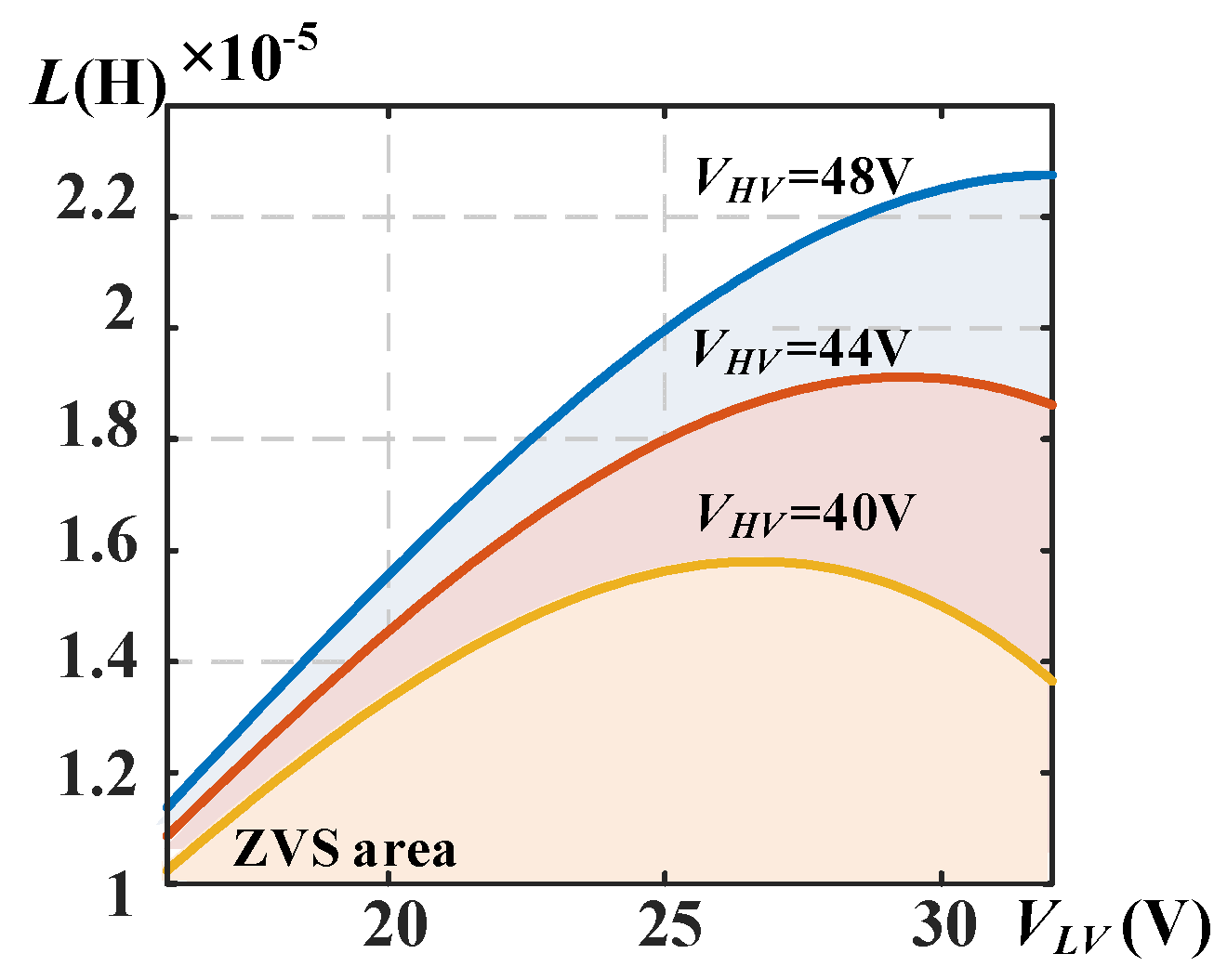
Figure 3 shows the required inductance values of the BCM over the whole load range. The condition of VHV = 48 V is plotted a as red line in Figure 3. For the different output voltage cases with a full load, the maximum allowable inductances are plotted in Figure 4. It can be seen that when the input voltage is low, the boost inductance values are at their lowest because the operating current is high. Therefore, the appropriate boost inductance value needs to be designed at a full load and at the lowest input voltage.

2.2. The Relationship between Switching Frequency and Switch Temperature

It can be deduced from the above analysis that there exists a high correlation between the switching frequency and the thermal factor. Thus, it is necessary to study the tradeoff between the switching frequency and the switching temperature. This part of the paper focuses on the corresponding temperature responses with the frequency of the semiconductor device in the bidirectional DC–DC converter using the OTC by introducing on an equivalent electro-thermal model of the power MOSFET.
The junction temperature of the MOSFET is customarily calculated using thermal resistance–capacitance (RC) networks that represent an equivalent of the heat transfer process from the chips to the heatsink, which can be described by the Fourier heat conduction equation:
q x = K A T x
where K—thermal conductivity; A—heat conduction area of the materials; qx—the heat produced or transmitted.
The Fourier heat conduction equation is a typical linear partial differential equation. The Cauer or Foster network can be used to model the heat conduction process. The Cauer network is more complex to use, which needs an scanning electron microscope (SEM) to analyze the material properties. However, the junction temperature is more important than the internal thermal distribution of the MOSFET chip is in this research. The Foster network was selected to fit the transient thermal resistance curve, as were four thermal resistance network layers of the model accuracy to achieve the rapid and accurate transient thermal resistance of the MOSFET.
Z t h ( t ) = i = 1 4 R t h i ( 1 e t R t h i C t h i )
The parameters of the Foster RC thermal model can be derived from a cooling curve and a curve fitting technique. The junction temperature of MOSFET can be expressed as:
T j = P l o s s × ( Z j c + Z c h + Z h a ) + T a
where Ploss—the total loss power. The detailed derivation of the total loss is given in the Appendix A. Zjc—the thermal impedance of the junction to the case. Zch—the thermal impedance between the case and the heat sink. Zha—the thermal impedance of the heat sink to the ambient environment.
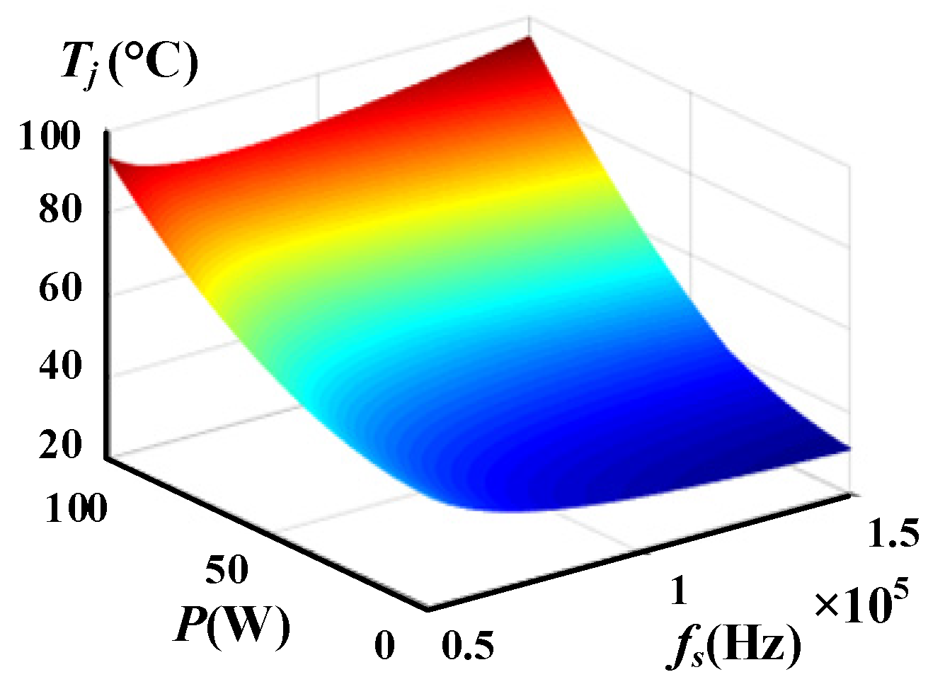
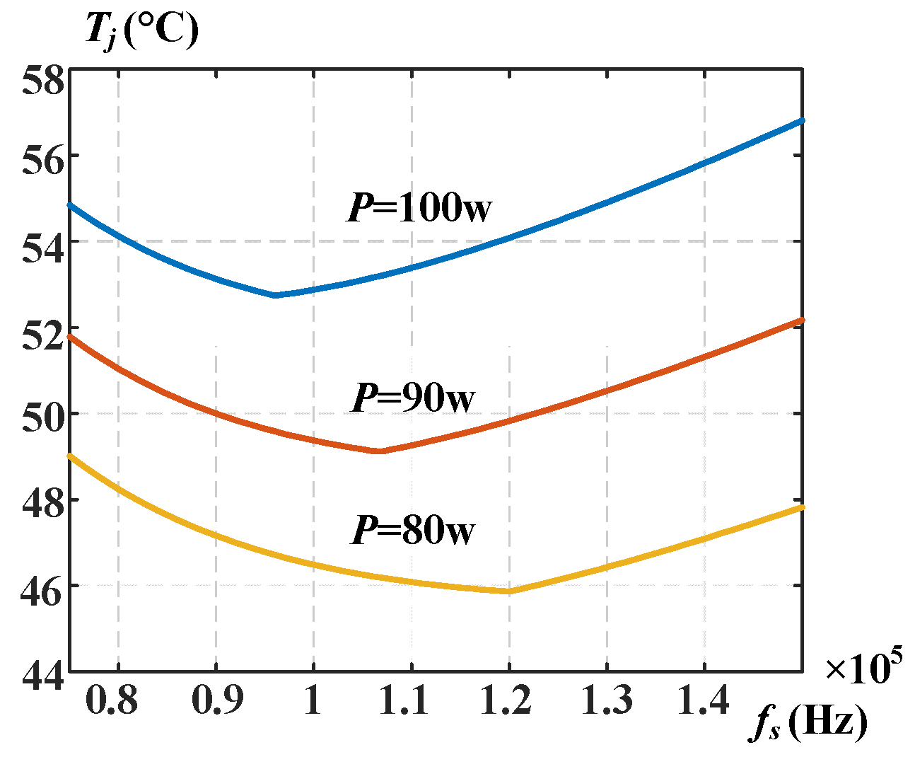
An extra negative current Imin requires a higher Imax to produce the same average current which will increase the conduction losses. Thus, the switching frequency must be properly chosen to obtain an ZVS with a minimum Imin. Figure 5 shows the junction temperature of the power device under a range of switching frequencies which were swapped at various loads. The dynamic nature of generating different power values and voltages according to the load conditions is the challenging factor in the field of DC/DC converters. The MOSFET in the boost circuit can operate at different switching frequencies, but only at certain switching frequencies can the MOSFET remain at the lowest operating junction temperature. The junction temperature versus switching frequency curves obtained from three fixed load condition is shown in Figure 6. For each load condition, the optimal switching frequency is not same.

3. Optimal Thermal-Based Adaptive Frequency Control

3.1. Optimal Temperature Control (OTC) Algorithm

The OTC for a bidirectional DC–DC converter with BCM can achieve a minimum junction temperature using the MOSFET by tracking the temperature of the power device under various conditions. In order to get the driver signal from the OTC, the turn-on and turn-off time of the MOSFET are figured out by a digital processor using the proposed algorithm. The switching frequency will be updated at a certain intervals based on the temperature feedback. This method operates without a current sensor or auxiliary ZCD circuits and instead, by directly measuring the junction temperature.
In this paper, the perturb and observe technique is used in the OTC algorithm since its offers simplicity and effectiveness. This algorithm perturbs the switching frequency to ensure that there is an optimal temperature. To make the MOSFET operate near the minimum temperature, the controlling methodology first detects the temperature using a temperature sensor. At an operating point on the Tjfs curve, if the switching frequency is adjusted in a given direction and ΔTj < 0, it is known that the perturbation will move the MOSFET’s operating point toward the optimal temperature point. ΔTj is the temperature difference of the previous step and the new step. Δfs is the switching frequency difference of the previous step and the new step. Operating on the left of the optimal temperature point, it is obvious that incrementing (or decrementing) the switching frequency allows one to decrease (or increase) the temperature and increase (or decrease) the temperature when it is on the other side, while if the ΔTj = 0, the switching frequency remains at the previous step. The detailed steps are as follows, as shown in Figure 7.
Step 1: The temperature of the power device at the present time Tj(k) is detected.
Step 2: Compare the temperature Tj(k) with the previous moment and calculate the difference between them, which is defined as ΔTj.
Step 3: Then, enter the part of judgement. The ΔTj is checked to determine if it is positive or negative.
Step 4: In addition, it is necessary to judge the variable in the frequency.
Step 5: If ΔTj is positive and the fs(k) ≥ fs(k − 1), then the frequency at k + 1 time should be reduced; if ΔTj is positive, but the fs(k) ≥ fs(k − 1) is not satisfied, then the frequency at k+1 time should be increased; if ΔTj is negative and the fs(k) ≥ fs(k − 1), then the frequency at k+1 time should be increased. On the contrary, if ΔTj is negative and the fs(k) ≥ fs(k − 1) is not satisfied, then the frequency at k + 1 time should be reduced.
Step 6: Once the switching period is calculated, the fs(k) must be checked to determine if it is in the available frequency range.
Step 7: The new switching frequency of MOSFET should be updated.

3.2. Simulation of Proposed Method

To verify the above analysis, the proposed controller design was initially implemented in PLECS. The power device under the test junction temperature is S1 because S2 always works with ZVS. The simulation parameters were the same as they are in the experimental design, which are listed in Table 1.
Figure 8 depicts a control block diagram of the proposed structure. The output voltage needed to be sampled. Then, the error value which next became a proportional integral was obtained by subtracting the output voltage from the reference voltage. The output of PI is the duty ratio D. On the other hand, the junction temperature had to be sampled and sent to the controller using the OTC. Thus, the optimal frequency based on the thermal factor can be calculated. Lastly, according to the duty ratio and optimal switching frequency, the driving signals of S1 and S2 were generated.
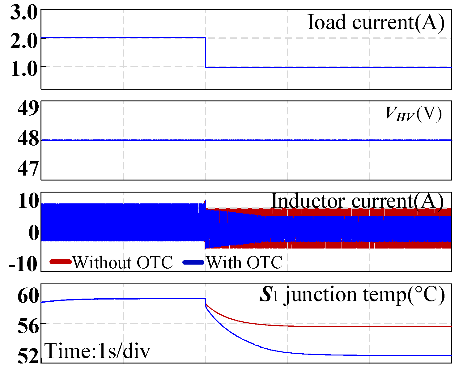
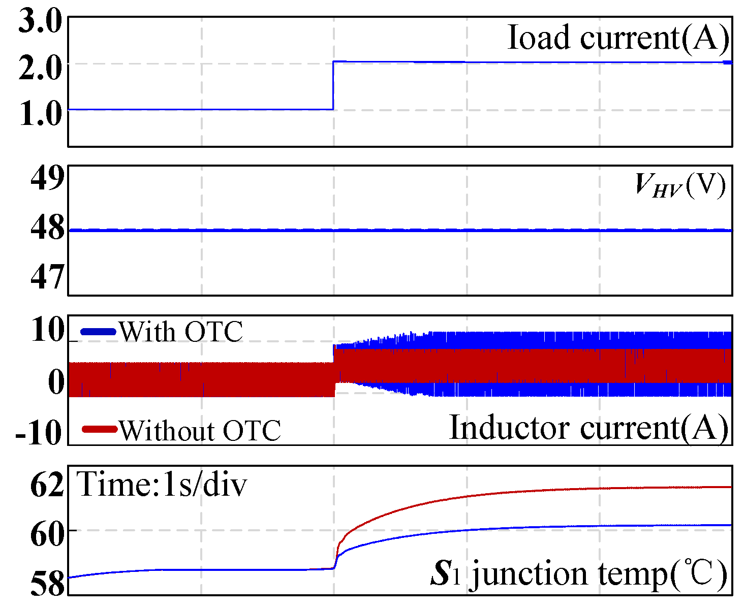
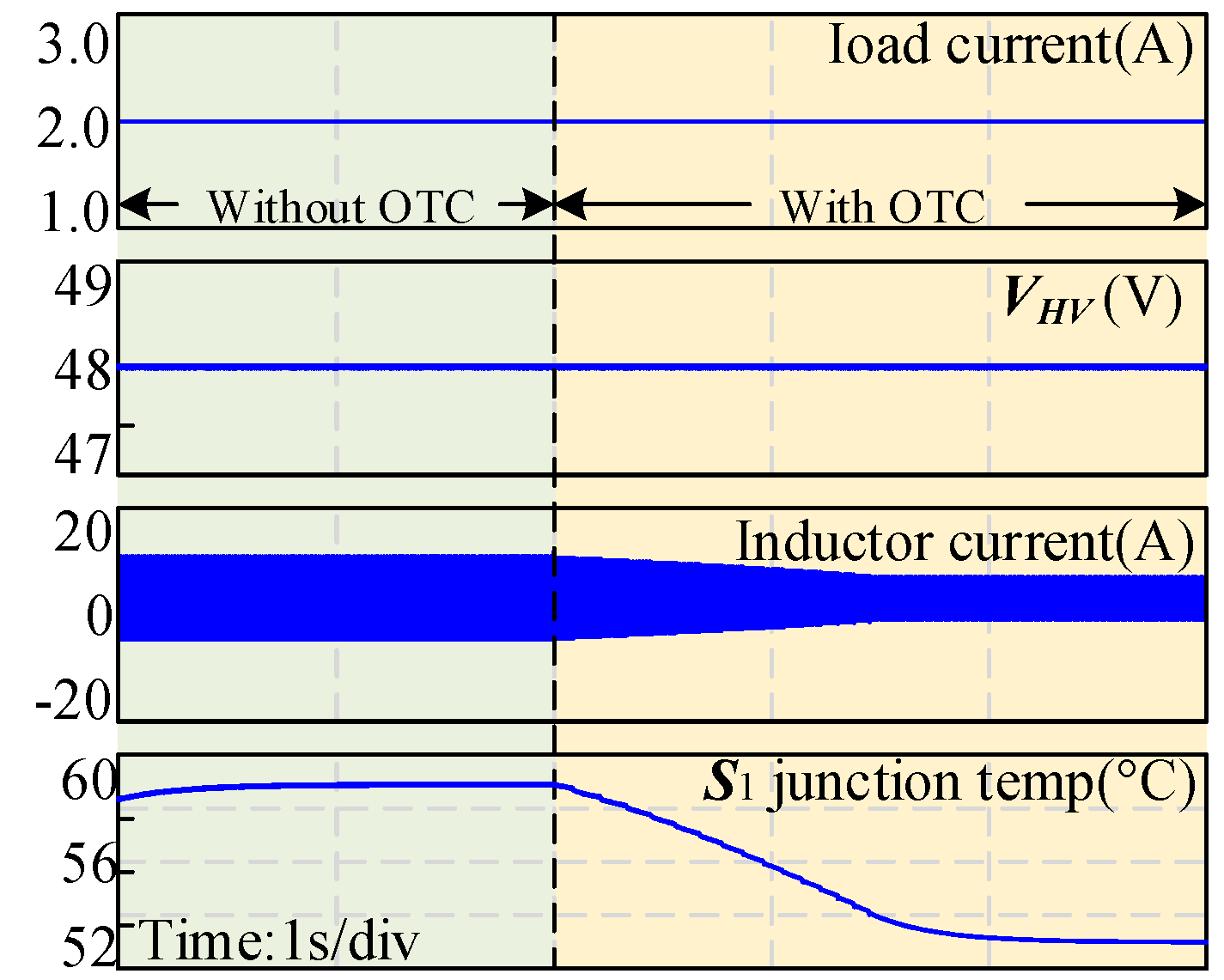
Figure 9 and Figure 10 show a comparison between the junction temperature ameliorations caused by the fixed switching frequency versus the proposed OTC algorithm, respectively; as it can be shown in the waveform, the OTC algorithm obtains a significant temperature reduction when it is compared with the fixed frequency method. From the full-load to half-load conditions, in Figure 9, the red line is operating without the OTC, and the blue line is operating with the OTC. As the curves show, a lower junction temperature was needed for it to operate with the OTC at the load condition change. On the other hand, Figure 9 shows that the junction temperature variation with the OTC is less than it is without the OTC between the half-load condition and the full-load condition. Figure 11 at VLV = 24 V, at full load, the optimum switching frequency was at 138 kHz with the OTC. Compared to the temperature that was achieved without the OTC, it was significantly reduced by the OTC. The simulation results show that the OTC achieves the lowest temperature according to the direct feedback of the temperature at different loads.

3.3. Conparison of ZVS Methods

A comparison of the different ZVS topologies and BCM control methods proposed for the DC–DC converter are shown in Table 2 and Table 3, respectively. The comparison of the topologies are made in terms of the number of switches, the passive components, soft switching, switching frequency, efficiency, and output range. It can be seen that the proposed variable switching frequency modulation can achieve a high efficiency without any auxiliary device being used. In Table 3, the four aspects of cost, complexity, accuracy, and response speed are compared. The accuracy of the ZCD circuit is higher than those of the others, while the cost is the same among them. The sensor-less method cost low, but it has a complex circuit. The digital control one and the proposed OTC seem to have more advantages. It can be seen that the proposed OTC has a simple structure and a low cost. However, it should be noted that the ZVS will be temporarily lost when the working state changes rapidly. The proposed OTC is suitable for cases such as a battery energy storage system, for which its operation is relatively stable.

4. Experiment

The performance of the proposed method was tested and evaluated on a 100 W bidirectional boost converter, as shown in Figure 12 with the parameters that are listed in Table 1. The digital microcontroller DSP was implemented to achieve both the proposed OTC method and the output voltage PI control.
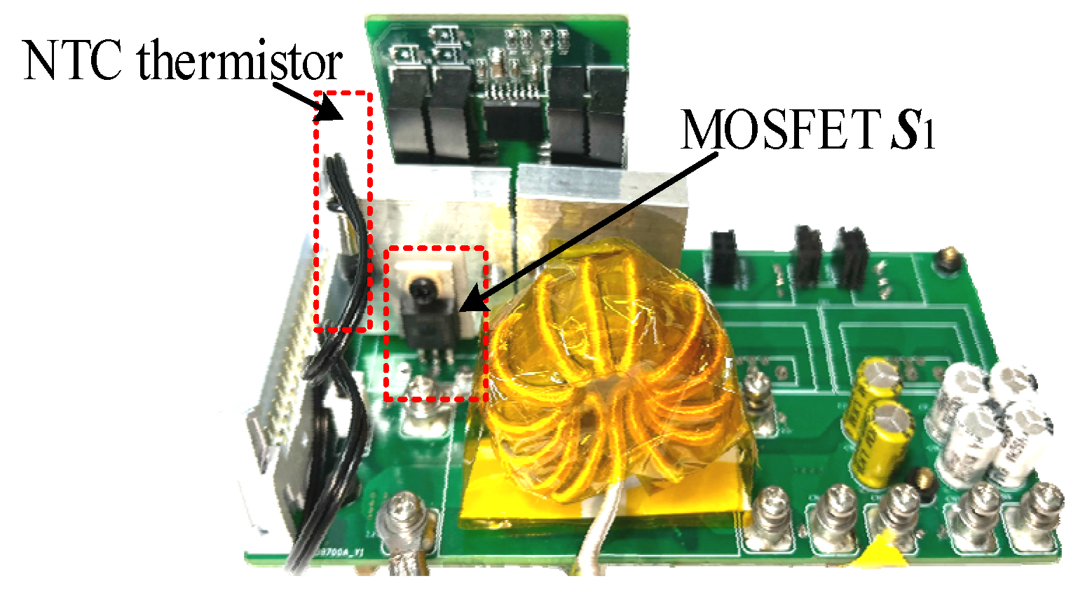
The indicator of the OTC is the temperature of the heat sink which was sensed by an NTC thermistor. To track the optimum temperature, the NTC thermistor feeds its measurement to the digital controller. Then, a new value of switching frequency is calculated.
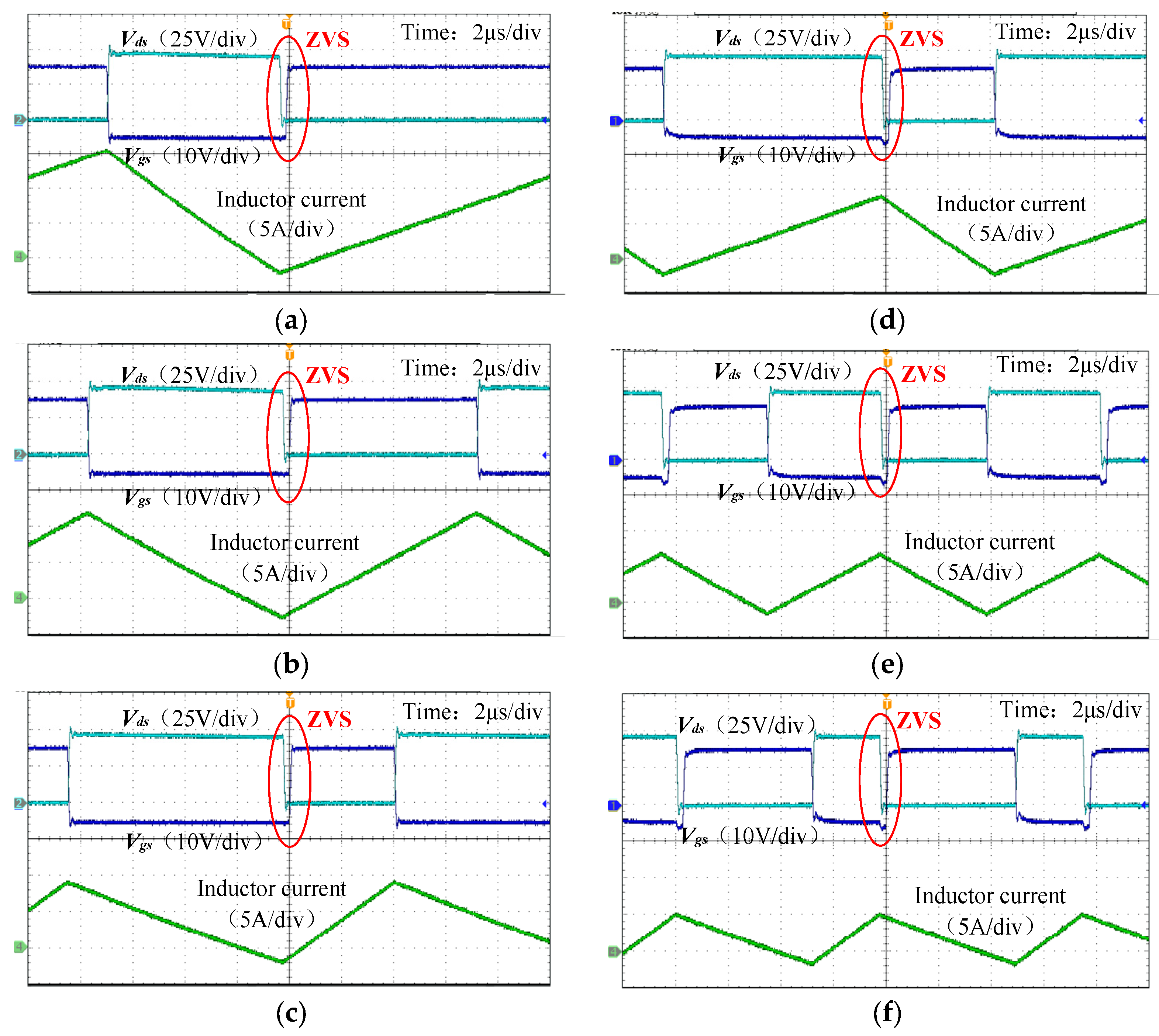
The steady-state operation waveforms with a full load are shown in Figure 13. It can be seen that under different input voltages (16, 24, and 32 V), the switching frequency was adjusted adaptively by the proposed OTC, and the minimum inductor current Imin was less than zero. In addition, the voltage Vds1 reached zero before the gate pulse Vgs1 was applicable to S1. Hence, S1 and S2 can both achieve the ZVS. In addition, according to the ZVS analysis, the full load is the worst case for the ZVS. It can be concluded that the full operation range ZVS can be achieved with the proposed control algorithm.
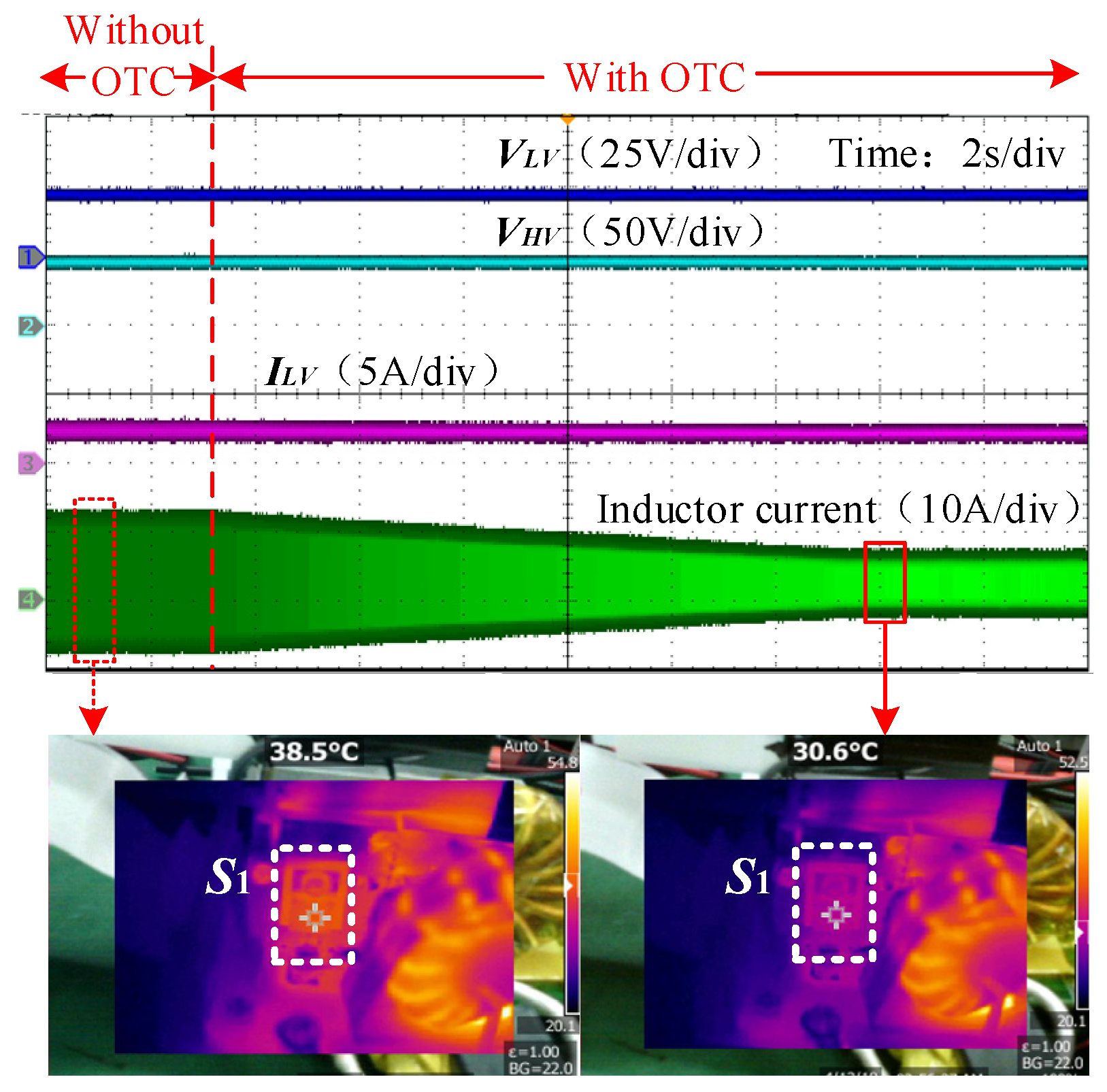
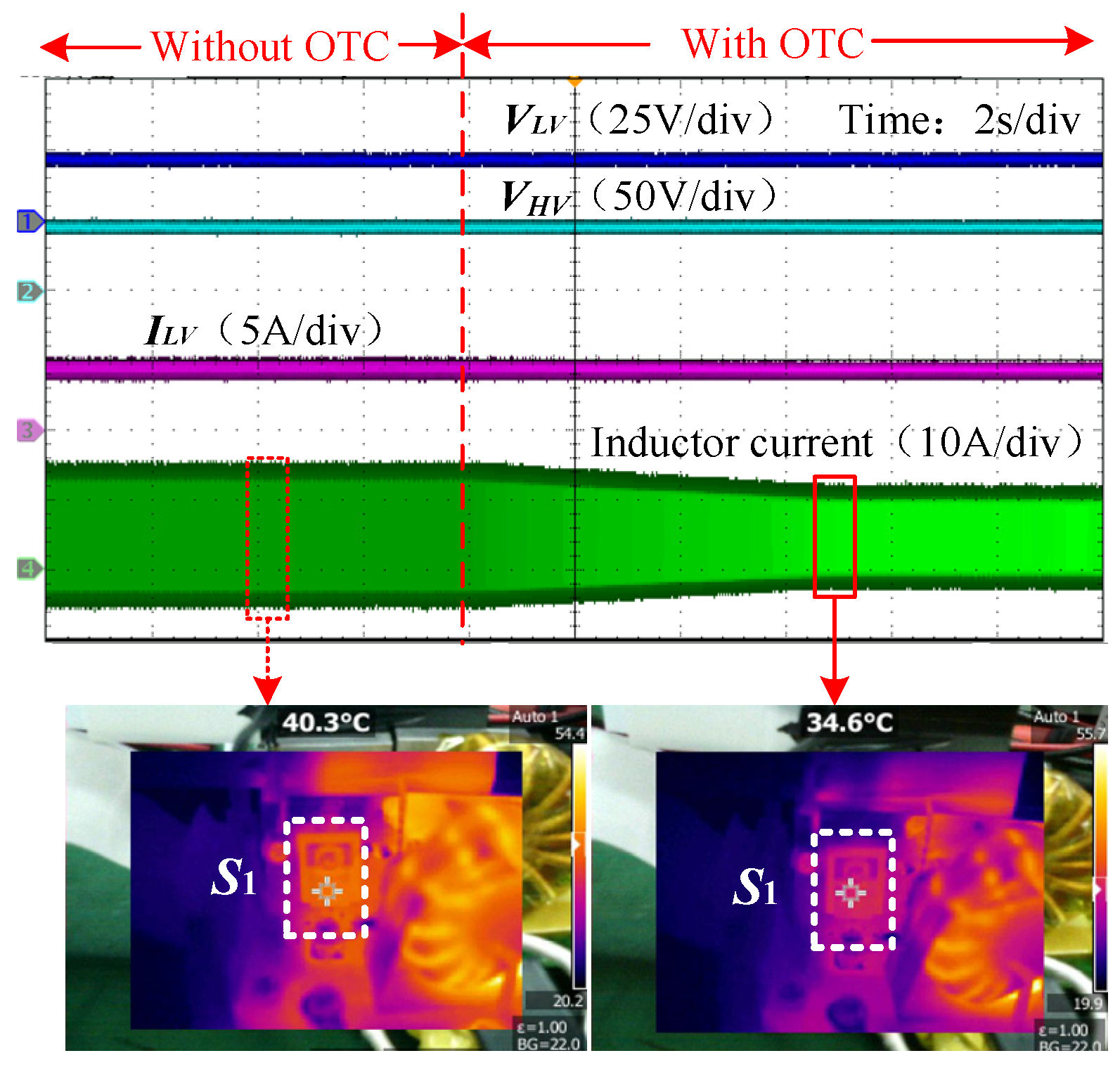
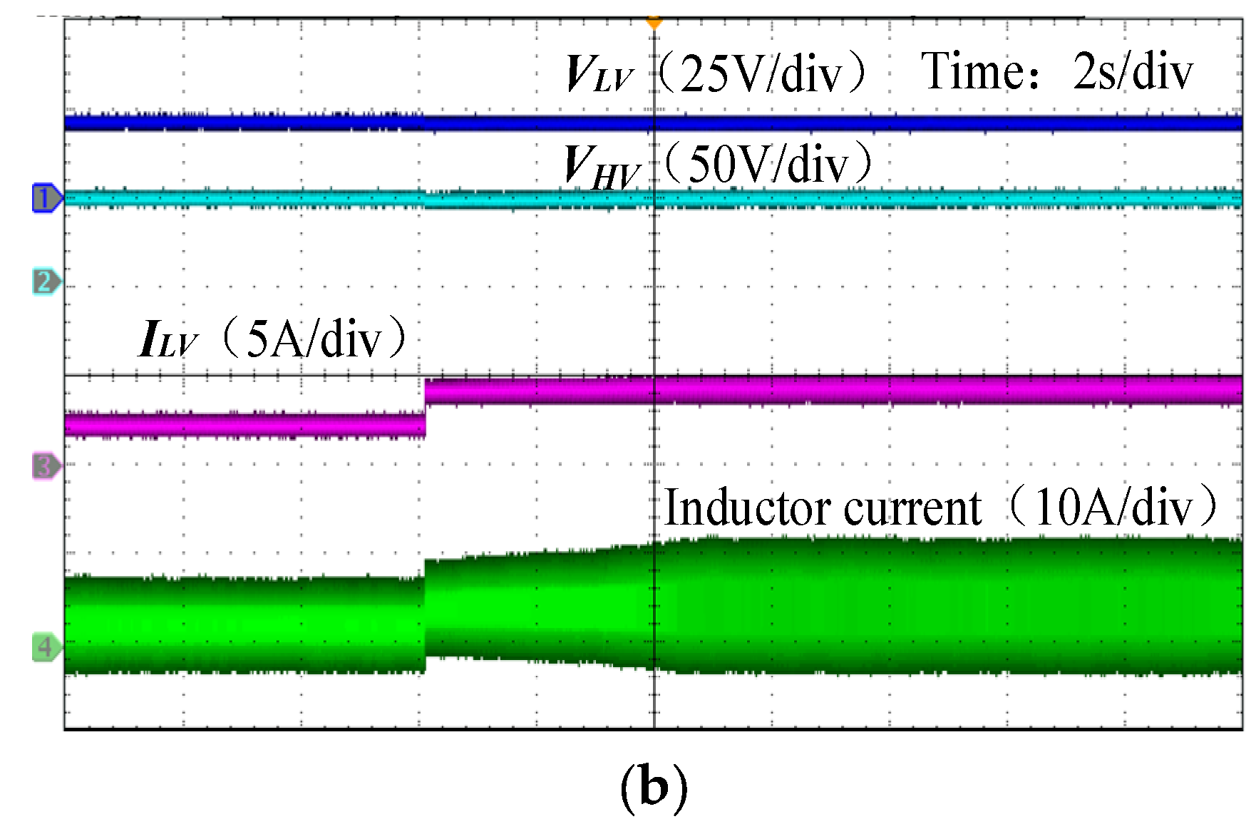
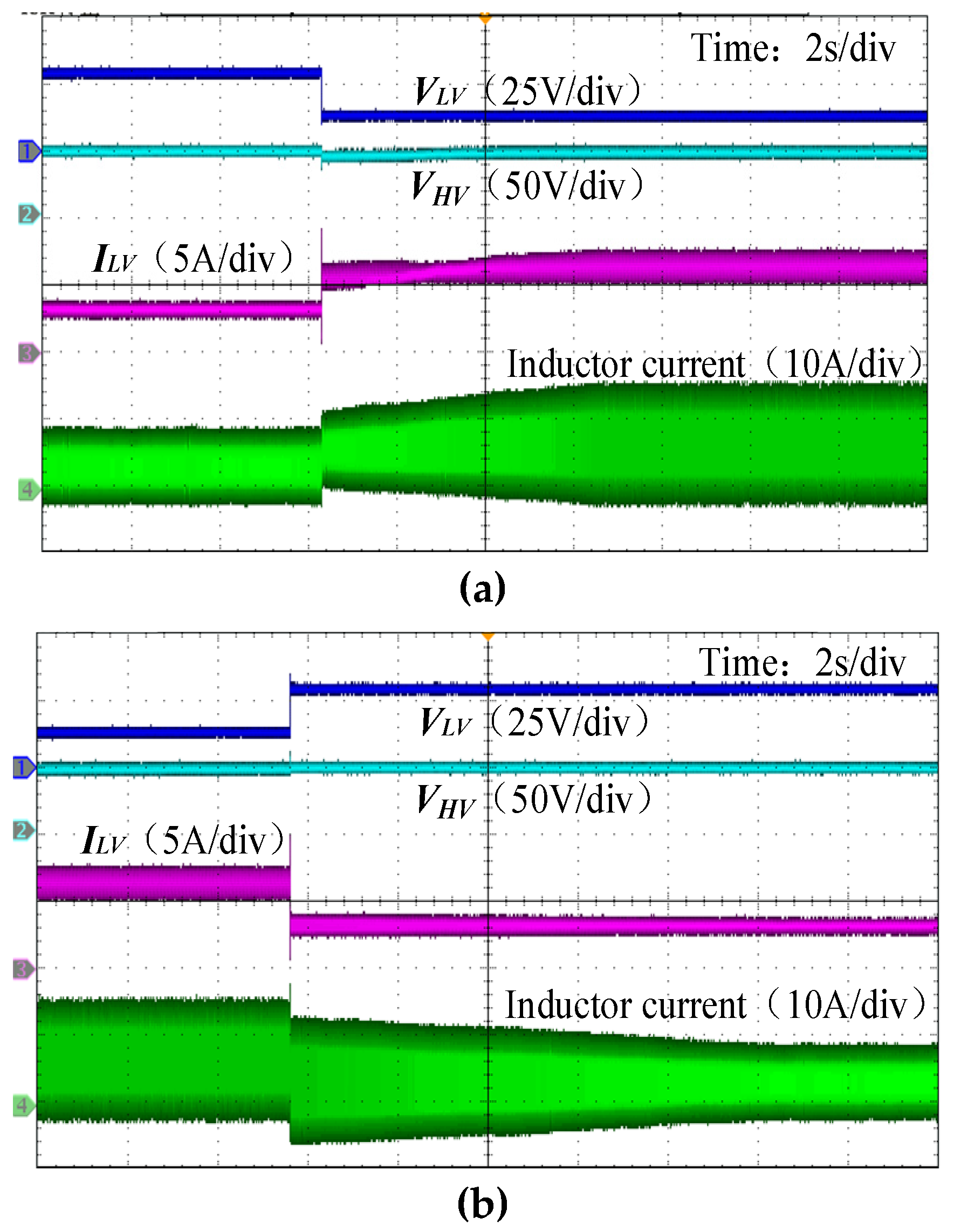
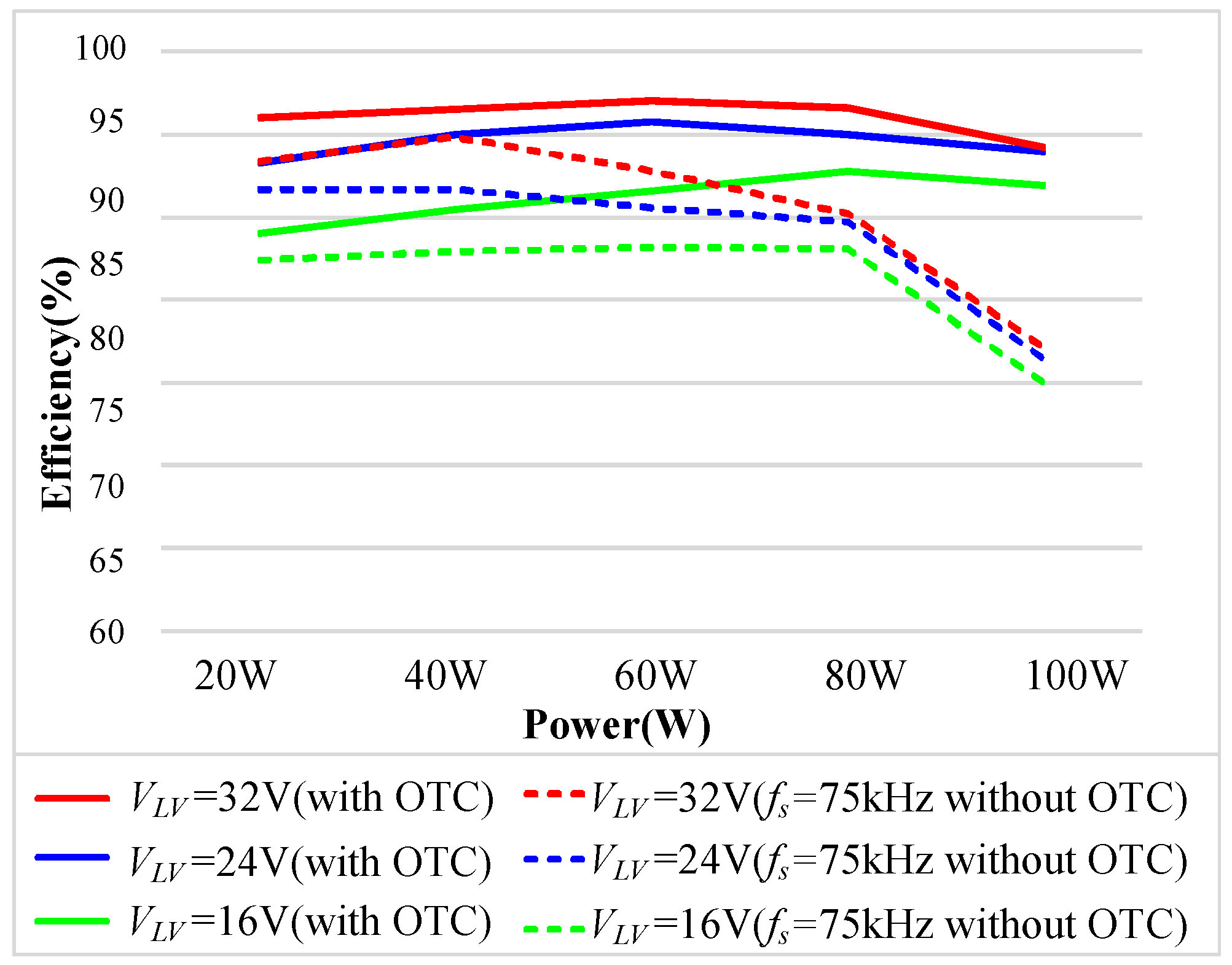
The dynamic waveforms of the OTC are shown in Figure 14, Figure 15 and Figure 16. The contrast waveforms of the proposed OTC are shown in Figure 14 and Figure 15. It can be seen that the inductor current ripple was reduced with the proposed OTC method. Additionally, the Imin was kept at less than zero. The case of the temperature of S1 with an optimal frequency is lower than the fixed frequency is, as shown in the thermal images. Figure 16 shows the dynamic response of the proposed OTC. In order to achieve a ZVS at a full load, the inductor current ripple is large, and the switching frequency is low. When the step to a half load state is taken, the switching frequency is increased, and the inductor current ripple is reduced by the proposed OTC. In addition, Figure 17 shows that when the input voltage changed, the frequency changed depending on the temperature. In Figure 18, the efficiency curves of the OTC and traditional method according to the load are shown, which presents the high efficiency that was achieved in the proposed OTC. Thus, the optimal frequency for the temperature can be tracked with various voltages and load conditions.

5. Conclusions

An optimal thermal-based adaptive frequency control (OTC) for bidirectional DC–DC converters has been proposed in this paper. This method directly adjusts the switching frequency by measuring the temperature. In addition, it can track the minimum temperature by adapting the optimal switching frequency which achieves a ZVS over a wide load variation. Additionally, the cost has been largely reduced by using the NTC thermistor without a ZCD or a current sensor. The effect on the thermal factor caused by switching the frequency and the feasibility of the optimal temperature digital controller under variable load conditions is analyzed in this paper. The proposed method is capable of significantly reducing the thermal of the power device and increasing the efficiency at any load value in the simulation and the experiment. It can protect the power module from failures resulting from having sustained operation temperatures. This new technology will be widely used in DC–DC converters to control the temperature effectively.

Author Contributions

Conceptualization, J.X.; data curation, C.X.; writing—original draft preparation, L.Z.; writing—review and editing, L.Z., J.X. and S.C.; funding acquisition, T.Y. and S.C. All authors have read and agreed to the published version of the manuscript.

Funding

This research was funded by the National Natural Science Foundation of China under Grant 52072414.

Data Availability Statement

Not applicable.

Conflicts of Interest

The authors declare no conflict of interest.

Appendix A

In the boost topology, MOSFET, as the main power device, will experience a considerable power losses. The MOSFET power losses mainly include conduction losses and switching losses. In forward power transmission, the device under analysis is S1 since S2 always turns on with zero voltages. S1 with a ZVS and without a ZVS will cause the differences in switching losses, and the switching losses depend on the switching frequency. Conduction losses are a function of the load current, and they are junction temperature dependent. Thus, a mathematical, temperature-dependent MOSFET power losses model of two conditions is proposed in this part.
  • Loss analysis of Imin > 0 (without ZVS)
D is duty ratio of the S1:
D = T o n T o n + T o f f
The ripple current of the input signal:
Δ i L = I max I min
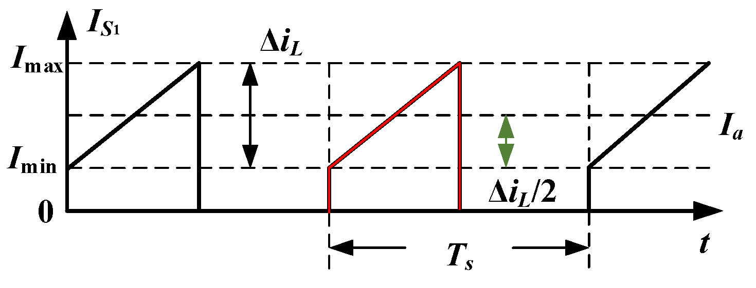
The average current of power device S1 is:
I a = 1 T 0 T o n I S 1 ( t )   d t
The integral part of the (A3) represents the area of the image that is enclosed by the input current I and the t-axis during the opening time.
When the current flowing through the MOSFET in the CCM mode is trapezoidal wave, as shown in the figure, the expression of current of S1 is:
Figure A1. The current waveform of S1 for Imin > 0 (without ZVS).
Energies 15 08250 g0a1
I S 1 = { I a Δ i L 2 + Δ i L T o n t ( 0 < t < T o n ) 0 ( T o n < t < T )
According to the definition of root-mean-square:
I r m s = 1 T 0 T o n I S 1 ( t ) d t = 1 T 0 T o n ( I a Δ i L 2 + Δ i L T o n t ) d t = D ( I a 2 + Δ i L 2 12 )
The conduction loss of the MOSFET refers to the loss that is generated by the current in the switching resistance during the conduction time. Conduction power losses are a function of the RMS currents’ squared values. The calculation formula of the conduction loss is as follows:
P c o n _ C C M = I r m s 2 R d s _ o n = D ( I a 2 + Δ i L 2 12 ) R d s _ o n
R d s _ o n = R d s _ o n 25 ( 1 + K d s ( T j 25 ) )
In the power loss estimation, the MOSFET on-state resistance Rds_on is the main parameter that is temperature dependent. Rds_on25 is the on-resistance at junction temperature of 25, which can be obtained from datasheet. We used an on-resistance vs. junction temperature curve to get an approximate ratio Kds.
Unlike the conduction loss, there is little temperature influence on the switching loss. The MOSFET switching losses include the turn on loss and the turn off loss. When the MOSFET is turned on, the drain–source voltage gradually decreases, and the drain current gradually increases. In this process, the overlapping parts are generated, which are the switching losses of the MOSFET. The switching power losses are a function of the switching frequency of the switches, the voltage across the switches, and current through the switches.
The drain–source voltage is:
v d s ( t ) = V H V V H V t r t
The drain current is:
i d s ( t ) = I min t r t
The turn on loss is:
P o n = f s 0 t r i d s ( t ) v d s ( t ) d t = 1 6 V H V ( I a Δ i L 2 2 ) t r f s
The turn off loss, as shown in the figure above, refers to the loss that is caused by the overlap of drain–source voltage rise and the drain current drop during the MOSFET turn off.
The drain–source voltage can be expressed as:
v d s ( t ) = V H V t f t
The drain current is determined as:
i d s ( t ) = I max I max t f t
Hence, the turn off loss can be calculated as:
P o f f = f s 0 t f i d s ( t ) v d s ( t ) d t = 1 6 V H V ( I a + Δ i L 2 ) t f f s
The reverse-recovery loss PQrr is as:
P Q r r = Q r r V L V f s
Qrr is the reverse recovery charge.
The total loss of the MOSFET in the Imin > 0 condition is:
P l o s s = P c o n + P o n + P o f f + P Q r r
2.
Loss analysis of Imin ≤ 0 (with ZVS)
When Imin ≤ 0, a ZVS operation mode is usually preferred, which allows a nearly lossless turn on, but as a consequence, there are losses during the turn off event. As long as the ZVS is reached, the current waveform on the inductor is different. The current flowing through the MOSFET is a triangular wave, as shown in Figure A2.
Figure A2. The current waveform of S1 for Imin ≤ 0.
Energies 15 08250 g0a2
When Imin ≤ 0, the turn-on loss is:
P o n = f s 0 t r i d s ( t ) v d s ( t ) d t = 1 6 V H V I min t r f s 0
The conduction loss and the turn-off loss are the same as the first condition:
P c o n _ C C M = I r m s 2 R d s _ o n = D ( I a 2 + Δ i L 2 12 ) R d s _ o n
P o f f = 1 6 V H V ( I a + Δ i L 2 ) t f f s
The total loss of MOSFET in Imin ≤ 0 condition is:
P l o s s = P c o n + P o f f + P Q r r

References

  1. Xu, Q.; Vafamand, N.; Chen, L.; Dragičević, T.; Xie, L.; Blaabjerg, F. Review on Advanced Control Technologies for Bidirectional DC/DC Converters in DC Microgrids. IEEE J. Emerg. Sel. Top. Power Electron. 2021, 9, 1205–1221. [Google Scholar] [CrossRef]
  2. Jiang, W.; Fahimi, B. Active Current Sharing and Source Management in Fuel Cell–Battery Hybrid Power System. IEEE Trans. Ind. Electron. 2010, 57, 752–761. [Google Scholar] [CrossRef]
  3. Zhang, C.; Xu, B.; Jasni, J.; Radzi, M.A.M.; Azis, N.; Zhang, Q. Model Control and Digital Implementation of the Three Phase Interleaved Parallel Bidirectional Buck–Boost Converter for New Energy Electric Vehicles. Energies 2022, 15, 7178. [Google Scholar] [CrossRef]
  4. Wu, H.; Sun, K.; Chen, L.; Zhu, L.; Xing, Y. High Step-Up/Step-Down Soft-Switching Bidirectional DC–DC Converter with Coupled-Inductor and Voltage Matching Control for Energy Storage Systems. IEEE Trans. Ind. Electron. 2016, 63, 2892–2903. [Google Scholar] [CrossRef]
  5. Shen, J.; Khaligh, A. A Supervisory Energy Management Control Strategy in a Battery/Ultracapacitor Hybrid Energy Storage System. IEEE Trans. Transp. Electrif. 2015, 1, 223–231. [Google Scholar] [CrossRef]
  6. Kim, N.-G.; Han, B.; Jo, S.-W.; Kim, M. High-Voltage-Gain Soft-Switching Converter Employing Bidirectional Switch for Fuel-Cell Vehicles. IEEE Trans. Veh. Technol. 2021, 70, 8731–8743. [Google Scholar] [CrossRef]
  7. Khan, M.A.; Ahmed, A.; Husain, I.; Sozer, Y.; Badawy, M. Performance Analysis of Bidirectional DC–DC Converters for Electric Vehicles. IEEE Trans. Ind. Appl. 2015, 51, 3442–3452. [Google Scholar] [CrossRef]
  8. Das, P.; Laan, B.; Mousavi, S.A.; Moschopoulos, G. A Nonisolated Bidirectional ZVS-PWM Active Clamped DC–DC Converter. IEEE Trans. Power Electron. 2009, 24, 553–558. [Google Scholar] [CrossRef]
  9. Hwang, T.; Park, S. Seamless Boost Converter Control Under the Critical Boundary Condition for a Fuel Cell Power Conditioning System. IEEE Trans. Power Electron. 2012, 27, 3616–3626. [Google Scholar] [CrossRef]
  10. Wu, H.; Lu, J.; Shi, W.; Xing, Y. Nonisolated Bidirectional DC–DC Converters with Negative-Coupled Inductor. IEEE Trans. Power Electron. 2012, 27, 2231–2235. [Google Scholar] [CrossRef]
  11. Chiang, C.; Chen, C. Zero-Voltage-Switching Control for a PWM Buck Converter Under DCM/CCM Boundary. IEEE Trans. Power Electron. 2009, 24, 2120–2126. [Google Scholar] [CrossRef]
  12. Qahouq, J.A.A.; Abdel-Rahman, O.; Huang, L.; Batarseh, I. On Load Adaptive Control of Voltage Regulators for Power Managed Loads: Control Schemes to Improve Converter Efficiency and Performance. IEEE Trans. Power Electron. 2007, 22, 1806–1819. [Google Scholar] [CrossRef]
  13. Lee, C.-S.; Oh, Y.-J.; Na, K.-Y.; Kim, Y.-S.; Kim, N.-S. Integrated BiCMOS Control Circuits for High-Performance DC–DC Boost Converter. IEEE Trans. Power Electron. 2013, 28, 2596–2603. [Google Scholar] [CrossRef]
  14. Yan, W.; Li, W.; Liu, R. A Noise-Shaped Buck DC–DC Converter with Improved Light-Load Efficiency and Fast Transient Response. IEEE Trans. Power Electron. 2011, 26, 3908–3924. [Google Scholar] [CrossRef]
  15. Panov, Y.; Jovanovic, M.M. Adaptive off-time control for variable frequency, soft-switched flyback converter at light loads. IEEE Trans. Power Electron. 2002, 17, 596–603. [Google Scholar] [CrossRef]
  16. Huang, Q.; Huang, A.Q. Variable Frequency Average Current Mode Control for ZVS Symmetrical Dual-Buck H-Bridge All-GaN Inverter. IEEE J. Emerg. Sel. Top. Power Electron. 2020, 8, 4416–4427. [Google Scholar] [CrossRef]
  17. Wang, K.; Zhu, H.; Wu, J.; Yang, X.; Wang, L. Adaptive Driving Scheme for ZVS and Minimizing Circulating Current in MHz CRM Converters. IEEE Trans. Power Electron. 2021, 36, 3633–3637. [Google Scholar] [CrossRef]
  18. Ren, X.; Zhou, Y.; Guo, Z.; Wu, Y.; Zhang, Z.; Chen, Q. Simple Analog-Based Accurate Variable On-Time Control for Critical Conduction Mode Boost Power Factor Correction Converters. IEEE J. Emerg. Sel. Top. Power Electron. 2020, 8, 4025–4036. [Google Scholar] [CrossRef]
  19. Liu, C.; Lee, H.; Liao, P.; Chen, Y.; Chung, M.; Chen, P. Dual-Source Energy-Harvesting Interface with Cycle-by-Cycle Source Tracking and Adaptive Peak-Inductor-Current Control. IEEE J. Solid-State Circuits 2018, 53, 2741–2750. [Google Scholar] [CrossRef]
  20. Zhang, X.; Chen, P.-H.; Okuma, Y.; Ishida, K.; Ryu, Y.; Watanabe, K.; Sakurai, T.; Takamiya, M. A 0.6 V Input CCM/DCM Operating Digital Buck Converter in 40 nm CMOS. IEEE J. Solid-State Circuits 2014, 49, 2377–2386. [Google Scholar] [CrossRef]
  21. Radić, A.; Straka, A.; Prodić, A. Synchronized Zero-Crossing-Based Self-Tuning Capacitor Time-Constant Estimator for Low-Power Digitally Controlled DC–DC Converters. IEEE Trans. Power Electron. 2014, 29, 5106–5110. [Google Scholar] [CrossRef]
  22. Michal, V. Inductor Current Zero-Crossing Detector and CCM/DCM Boundary Detector for Integrated High-Current Switched-Mode DC–DC Converters. IEEE Trans. Power Electron. 2014, 29, 5384–5391. [Google Scholar] [CrossRef]
  23. Kim, J.; Shim, M.; Jung, J.; Kim, H.; Kim, C. A DC–DC Boost Converter with Variation Tolerant MPPT Technique and Efficient ZCS Circuit for Thermoelectric Energy Harvesting Applications. In Proceedings of the 2014 19th Asia and South Pacific Design Automation Conference (ASP-DAC), Singapore, 20–23 January 2014; pp. 35–36. [Google Scholar]
  24. Liu, Y.-C.; Syu, Y.-L.; Dung, N.A.; Chen, C.; Chen, K.-D.; Kim, K.A. High-Switching-Frequency TCM Digital Control for Bidirectional-Interleaved Buck Converters Without Phase Error for Battery Charging. IEEE J. Emerg. Sel. Top. Power Electron. 2020, 8, 2111–2123. [Google Scholar] [CrossRef]
  25. Baek, J.; Choi, W.; Cho, B. Digital Adaptive Frequency Modulation for Bidirectional DC–DC Converter. IEEE Trans. Ind. Electron. 2013, 60, 5167–5176. [Google Scholar] [CrossRef]
  26. Reverter, F.; Gasulla, M. Optimal inductor current in boost DC/DC converters regulating the input voltage applied to low-power photovoltaic modules. IEEE Trans. Power Electron. 2017, 32, 8. [Google Scholar] [CrossRef] [Green Version]
  27. Wang, J.-M.; Wu, S.-T. A Synchronous Buck DC–DC Converter Using a Novel Dual-Mode Control Scheme to Improve Efficiency. IEEE Trans. Power Electron. 2017, 32, 9. [Google Scholar] [CrossRef]
  28. Reverter, F.; Gasulla, M. Optimal inductor current in boost DC/DC converters operating in burst mode under light-load conditions. IEEE Trans. Power Electron. 2016, 31, 15–20. [Google Scholar] [CrossRef] [Green Version]
  29. Konjedic, T.; Korošec, L.; Truntič, M.; Restrepo, C.; Rodič, M.; Milanovič, M. DCM-Based Zero-Voltage Switching Control of a Bidirectional DC–DC Converter with Variable Switching Frequency. IEEE Trans. Power Electron. 2016, 31, 3273–3288. [Google Scholar] [CrossRef]
  30. Sankaranarayanan, V.; Gao, Y.; Erickson, R.W.; Maksimovic, D. Online Efficiency Optimization of a Closed-Loop Controlled SiC-Based Bidirectional Boost Converter. IEEE Trans. Power Electron. 2022, 37, 4008–4021. [Google Scholar] [CrossRef]
  31. Vazquez, A.; Martin, K.; Arias, M.; Sebastian, J. Variable-Width Hysteretic Analog Control for QSW-ZVS and TCM Source/Sink Converters. IEEE Trans. Power Electron. 2020, 35, 3. [Google Scholar] [CrossRef]
  32. Lazar, M.C.; Shreelakshmi, M.P. Efficient Bidirectional DC-DC Converter Using Digital Adaptive Frequency Modulation. In Proceedings of the 2021 IEEE International Power and Renewable Energy Conference (IPRECON), Kerala, India, 24–26 September 2021; pp. 1–6. [Google Scholar]
  33. Wang, J.-M.; Wu, S.-T. Sensorless control scheme for synchronous buck converter. IET Circuits Devices Syst. 2016, 10, 181–191. [Google Scholar] [CrossRef]
  34. Abu Qahouq, J.A. Control Scheme for Sensorless Operation and Detection of CCM and DCM Operation Modes in Synchronous Switching Power Converters. IEEE Trans. Power Electron. 2010, 25, 2489–2495. [Google Scholar] [CrossRef]
  35. Waffler, S.; Kolar, J.W. A Novel Low-Loss Modulation Strategy for High-Power Bidirectional Buck Boost Converters. IEEE Trans. Power Electron. 2009, 24, 6. [Google Scholar] [CrossRef]
  36. Park, C.; Choi, S. Quasi-Resonant Boost-Half-Bridge Converter with Reduced Turn-Off Switching Losses for 16 V Fuel Cell Application. IEEE Trans. Power Electron. 2013, 28, 11. [Google Scholar] [CrossRef]
  37. Wu, T.-F.; Lai, Y.-S.; Hung, J.-C.; Chen, Y.-M. Boost Converter with Coupled Inductors and Buck–Boost Type of Active Clamp. IEEE Trans. Ind. Electron. 2008, 55, 1. [Google Scholar] [CrossRef]
Figure 1. Topology of bidirectional converter.
Energies 15 08250 g001
Figure 2. Waveforms of bidirectional converter with two conditions (a) Imin ≤ 0 (with ZVS) and (b) Imin > 0 (without ZVS).
Energies 15 08250 g002
Figure 3. Critical inductance to operate in BCM with full load. The red line is the value of inductor VHV = 48 V.
Energies 15 08250 g003
Figure 4. Critical inductance to operate in BCM with three different output voltage cases.
Energies 15 08250 g004
Figure 5. Operating junction temperature of power device.
Energies 15 08250 g005
Figure 6. Tj–fs curve with different load power.
Energies 15 08250 g006
Figure 7. Flowchart of the proposed control algorithm.
Energies 15 08250 g007
Figure 8. The proposed control block diagram.
Energies 15 08250 g008
Figure 9. Simulation waveforms of 24 V input voltage to 48 V output voltage for a load current step from 2 A to 1 A with 100 W rated power.
Energies 15 08250 g009
Figure 10. Simulation waveforms of 24 V input voltage to 48 V output voltage for a load current step from 1 A to 2 A with 100 W rated power.
Energies 15 08250 g010
Figure 11. Simulation waveforms of the case that is being studied (24 V input voltage to 48 V output voltage with full load 100 W for fixed switching frequency convert to adaptive switching frequency).
Energies 15 08250 g011
Figure 12. Experimental prototype of a bidirectional boost converter.
Energies 15 08250 g012
Figure 13. Experimental ZVS waveforms of the S1. (a) VLV = 16 V, full load; (b) VLV = 24 V, full load; (c) VLV = 32 V, full load. Experimental ZVS waveforms of the S2. (d) VLV = 16 V, half load; (e) VLV = 24 V, half load; (f) VLV = 32 V, half load.
Energies 15 08250 g013
Figure 14. Experimental waveforms in VLV = 24 V, half load.
Energies 15 08250 g014
Figure 15. Experimental waveforms in VLV = 24 V, full load.
Energies 15 08250 g015
Figure 16. Experimental ZVS waveforms with (a) full-load step to half-load step in VLV = 24 V; (b) half-load step to full-load step in VLV = 24 V.
Energies 15 08250 g016aEnergies 15 08250 g016b
Figure 17. Experimental ZVS waveforms with (a) VLV = 32 V step to 16 V step; (b) VLV = 16 V step to 32 V step.
Energies 15 08250 g017
Figure 18. Experimental efficiency at different load comparison between OTC and traditional methods.
Energies 15 08250 g018
Table 1. Parameters of the experimental prototype and simulation.
Designed ParametersValue
Input voltage (VLV)16–32 V
Output voltage (VHV)48 V
Rated power (P)100 W
Inductance (L1)10 μH
Core typeKool Mµ
Capacitance (C)100 μF
PI controllerKp = 0.28, Ki = 2
MOSFETIPP200N15N3G
Switching frequency75–150 kHz
Table 2. The comparison with previous works.
TopologiesTraditional Boost Converter [35]Active Clamping Boost Converter [36]Quasi Resonant Boost Converter [37]Bidirectional Converter in This Paper
Number of switches1 MOSFET
1 Diode
2 MOSFET
1 Diode
1 MOSFET
1 Diode
2 MOSFET
0 Diode
Passive component3342
Soft switchingCCM/DCMCCM/DCMCCM/DCMBCM
Switching frequencyFixed frequencyFixed frequencyFixed frequencyVariable frequency
EfficiencyLowHighHighHigh
Output rangeWideMediumMediumWide
Table 3. The comparison of BCM controls.
MethodZCD [12,13,14,15,16]Digital Control [24,25,26,27,28,29,30,31,32]Sensorless [33,34]Proposed OTC
CostHighMediumLowLow
ComplexityHighMediumHighLow
AccuracyHighLowLowMedium
Response speedHighMediumMediumLow
Publisher’s Note: MDPI stays neutral with regard to jurisdictional claims in published maps and institutional affiliations.