Article

A Transformerless AC-AC Converter with Improved Power Quality Employed to Step-Down Power Frequency at Output

1
Department of Electrical Engineering, The University of Lahore, Lahore 54000, Pakistan
2
Department of Electrical Engineering, College of Engineering, Taif University, Taif 21944, Saudi Arabia
3
Department of Electrical and Computer Engineering, College of Engineering and Information Technology, Ajman University, Ajman 346, United Arab Emirates
4
Department of Electrical and Computer Engineering, Faculty of Engineering and Applied Science, Memorial University of Newfoundland, St. John’s, NL A1B 3X5, Canada
*
Author to whom correspondence should be addressed.
Energies 2022, 15(2), 667; https://doi.org/10.3390/en15020667
Submission received: 18 December 2021 / Revised: 13 January 2022 / Accepted: 14 January 2022 / Published: 17 January 2022

Abstract

:
Variable voltage and frequency are required to govern the torque-speed characteristics of many industrial drive systems. Traditionally, this is achieved with a power converting system implemented with multistage converters. This technology is based on rectifying AC power into DC and then DC into AC with an inverter circuit. The power quality concerns of both conversion stages are tackled by selecting high switching frequency PWM control and harmonics mitigation filters. Also, using a bulky DC-link capacitor is one of the big sources of low system reliability, so this approach increases the conversion losses, circuit, and control complications. The frequency step-down conversion is very attractive with direct AC-AC converters as it has a simple control and circuit structure, but these converters face poor power quality challenges once the output frequency is decreased with respect to an input. In these converters, the total harmonic distortion (THD) of the output voltage becomes very poor once the output frequency is reduced. The problem of high THD of the output is addressed in the power converting circuits implemented with line frequency multi-winding transformers. The required number of output winding and switching devices (diodes and thyristors) increases once the value of the output frequency is decreased. This will increase the overall volume, cost, and losses. The use of a bulky and costly line frequency transformer may be eliminated if AC voltage controllers have non-inverted and inverted voltage buck capabilities, such existing topologies either have complex control schemes or require a large number of operating devices. Therefore, in this research article, a new transformerless frequency step-down converter employing fewer devices is proposed. This approach is realized with a high-frequency controlled rectifier for the required voltage stabilization and a low-frequency inverter bridge for frequency control. Its validation is supported by the results attained from Simulink and practical-based prototypes.

1. Introduction

The electric power supplied by the utility grid to an end-user has a constant voltage (rms value) and frequency. This power characteristic cannot be directly employed for specific loads such as electric traction systems, induction heating processes, and variable speed industrial drive systems [1,2,3,4]. In these applications, controlling the voltage and frequency is a compulsory requirement. The conventional way for achieving this is an indirect conversion of electrical power based on rectification of AC into DC by employing voltage-controlled or uncontrolled approaches and inverters to obtain regulated AC from DC power [5,6,7]. With an uncontrolled rectification scheme, the voltage of the DC-link capacitor may be made controllable by employing DC-to-DC voltage regulating systems [8]. This approach has however several limitations, including high circuit volume, losses, and cost. These issues may be resolved with the other approach for regulating a DC-link capacitor that includes a controlled rectifier circuit, but this scheme is the main source of the harmonics injection in the input supply system. Complicated filtering schemes must be implemented to eliminate the dominant harmonics [9]. A high-frequency inverter with various control schemes provides the high-quality controllable AC voltage and frequency required by the loads. The power quality of this stage is also maintained at an acceptable range with the help of harmonic suppression filters. This power conversion method is complicated and is not favorable as its implantation requires a multilevel conversion process [10,11,12].
The control of voltage and frequency in a single-level conversion approach is attractive as it is simple to implement with a small size and reduces the cost. Here the control of output voltage is achieved by adjusting the input voltage with the proper on and off operation of the semiconductor devices. Most of the traditional commercially developed AC-AC frequency regulators used in electric traction systems [13], rolling and grinding processes [14] are based on the thyristors or Triac switching operation. The turn-off process of these devices is obtained through the line commutation approach. Although these power converters have high power capabilities, in this process, dominant generated harmonics are low-frequency, as reported in [15]. The conversion losses of thyristors-based operating topologies are high as they have high internal resistance and voltage. These schemes are mostly employed to reduce the input or grid frequency at the output.
The stabilization of the frequency at the output may also be attained with the high-frequency operation of the semiconductor devices. This target is achieved using PWM control that may invert or non-invert the input with voltage regulation features. Such schemes have two categories, in which one requires the use of the z-source configuration, and the other one is employed without this structure. The first approach is very inefficient and undesirable as its implementation needs a large number of devices and components [16]. This makes it challenging to control the dynamic behavior as this sort of system has high order. High cost and large size are the other aspects of this system. Non-z-source power converting approaches are gaining more attention nowadays as they have no such issues [17,18,19]. These techniques are further classified as frequency regulation with and without voltage regulation features [20,21,22]. The frequency stabilization schemes stated in [19] have voltage regulation features, but their control strategies are non-identical to obtain the non-inverted and inverted forms of the input voltage at the output. The control schemes stated in [23] introduce a new circuit to ensure the symmetric nature of the control process, but their employment needs the use of a high number of switching devices. In the second approach, a power converter that only facilitates frequency stabilization (high or low) has easy and simple control approaches. Also, their implementation needs fewer electronic devices and components, but their output power quality is low, especially once the output frequency is almost one-third or one-fourth of the input frequency [
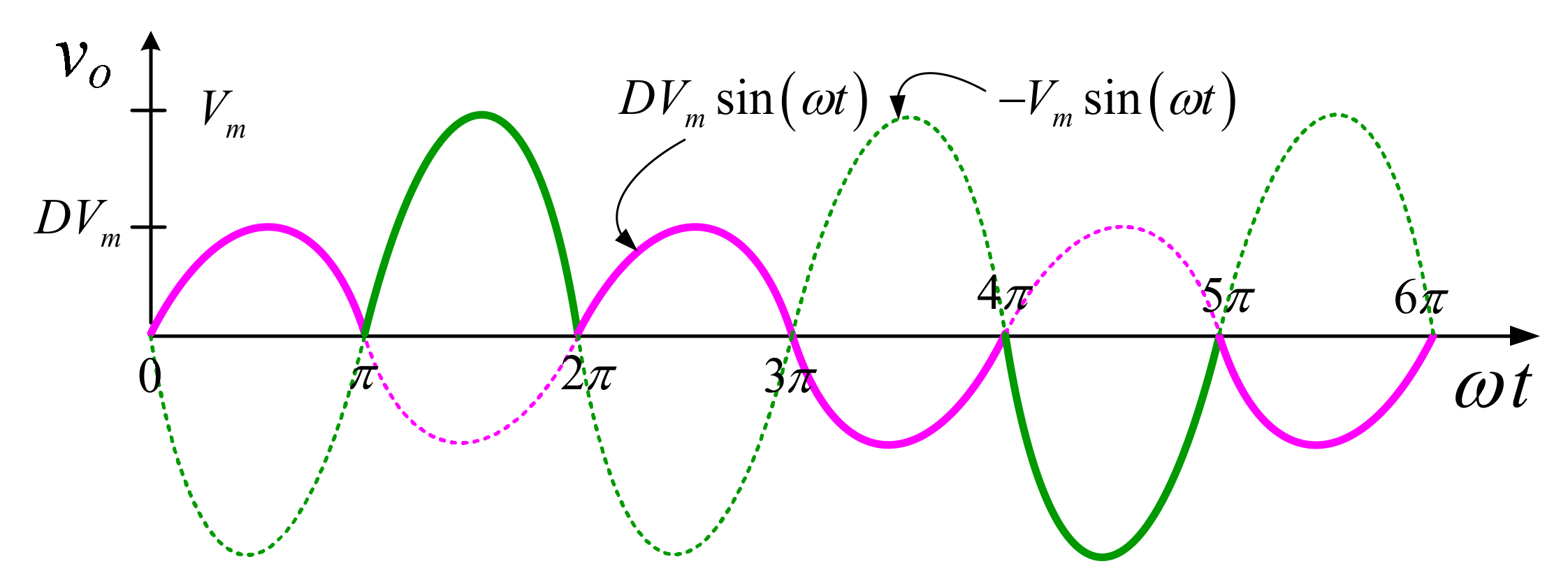
24]. The total harmonic distortion (THD) of such output voltage waveforms becomes more worsen than a square waveform of the output voltage that is approximately 48%. A new approach is developed in [25] shown in Figure 1 to address and tackle such issues. This circuit facilitates to attain the output pulses with the peak of ± V m / 2 and ± V m but this solution requires the use of a line frequency multi-winding transformer to change the instantaneous values of the selected output pulses. In any operating interval, one thyristor and one diode turn on to obtain the required form of the output. Their low-frequency on and off behavior is the main source of high conduction losses. The level in the output voltage is proportional to the number of winding and semiconductor devices. The application of a line frequency transformer with multi-winding is the main source of high volume, losses, and cost. The number of operating devices and their gate controller increases as the output voltage level is required to be increased.
This research article introduces a new direct frequency regulator by eliminating the use of the line frequency transformer with a fixed number of semiconductor devices. The various levels in the output pulses are ensured with the help of the voltage control process obtained from the PWM control of operating transistors. The required voltage level is based on the analysis of the generated harmonics. This solution reduces the overall circuit’s volume, losses, and cost.
This research article is organized by introducing the developed configuration and its operation in Section 2. Section 3 explores the power quality analysis of the various forms of the output voltage. Its performances are investigated and compared in Section 4. The experimental and simulation results are described in Section 5. Section 6 addresses the conclusions of the work.

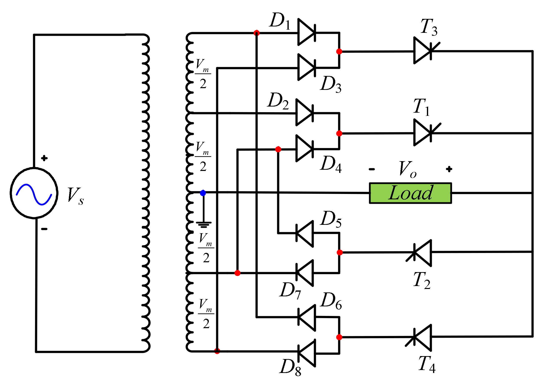
2. Developed Circuit and Operation

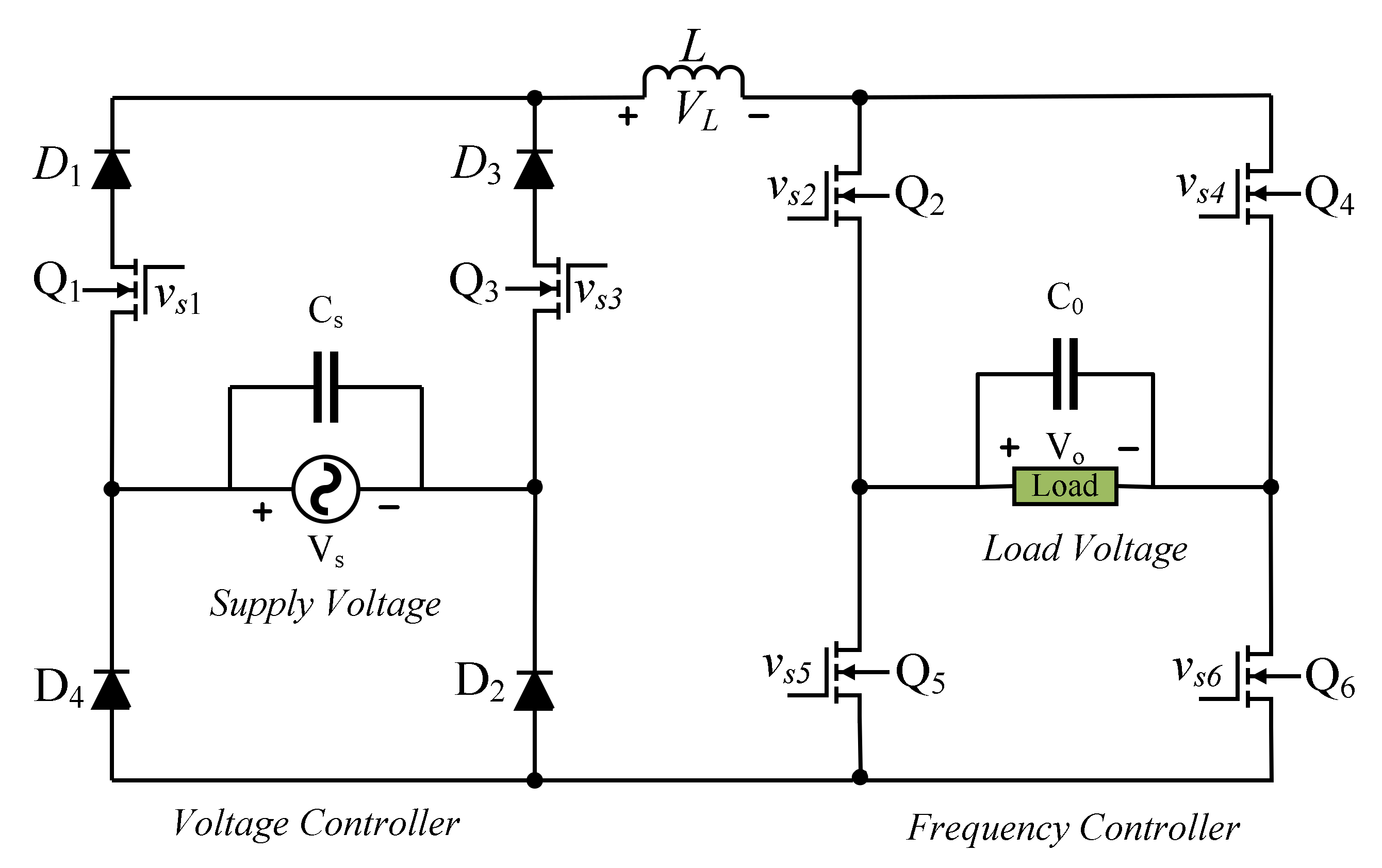
The created circuit capable of governing the output frequency and voltage is shown in Figure 2. This circuit is obtained by adding two more high switching transistors to the converter we developed in [22].
Six transistors and four diodes are used as switching devices along with one filtering inductor and two capacitors in its construction. This circuit can regulate the load voltage and frequency in a separate control. The voltage control circuit is responsible for governing the instantaneous or peak value of the selected output pulses by employing PWM control. The power quality criterion of output is maintained at the required level by selecting the appropriate switching frequency once the voltage regulation is needed. Otherwise, all the semiconductor elements operate at low grid frequency.
The voltage controller circuit (constructed with transistors Q1, Q3 and diodes D1 to D4) regulates the selected pulses. It converts the regulated and non-regulated voltage pulses into their absolute form. For this purpose, the transistors Q1 and 
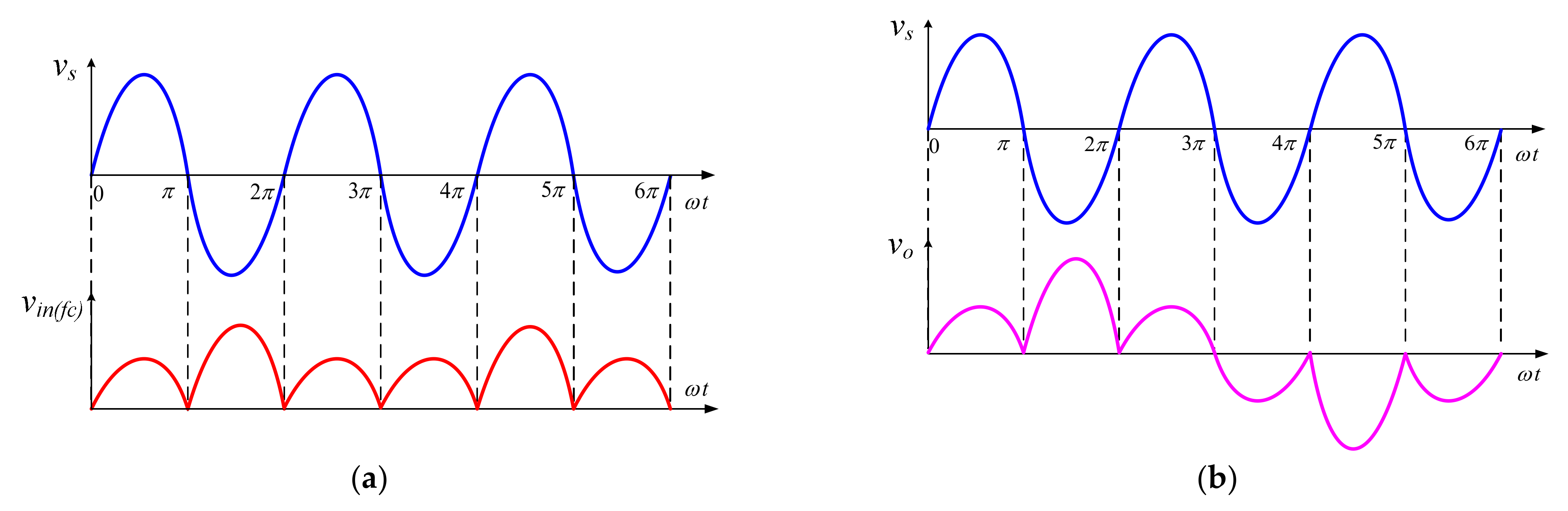
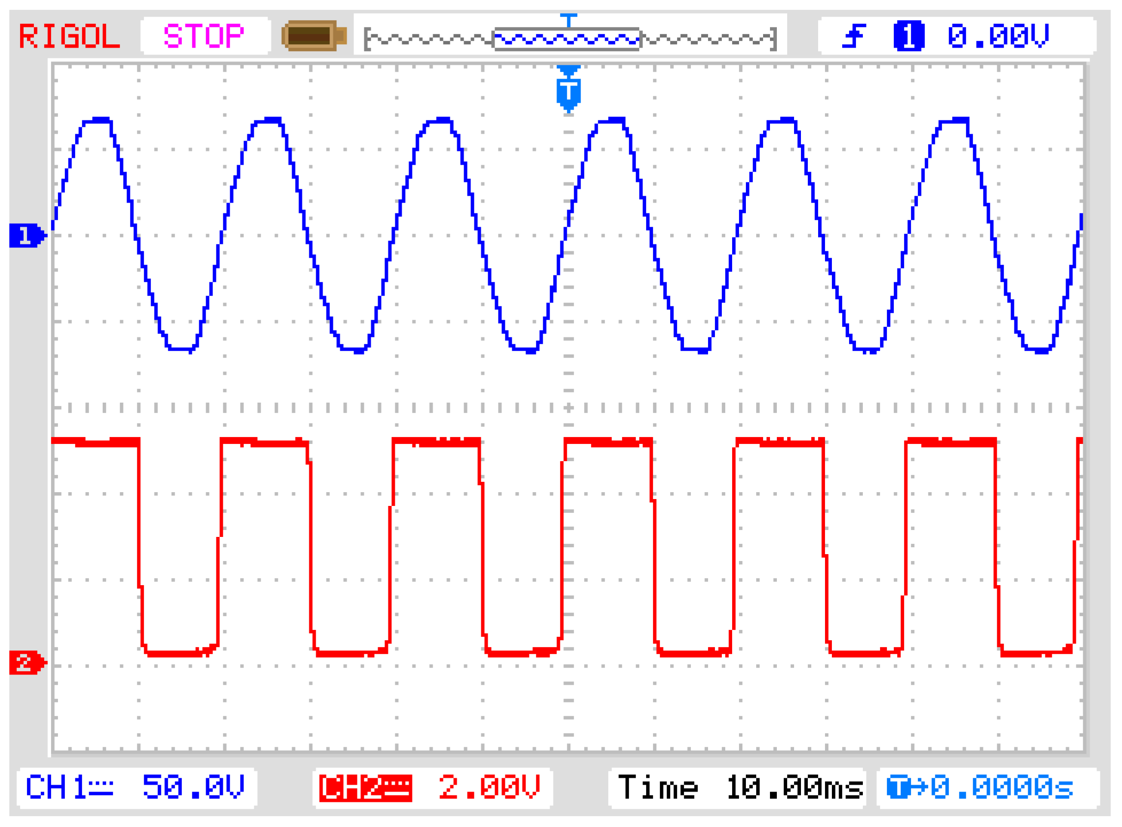
Q3 operate with PWM control once voltage regulation is desirable otherwise their role is to operate at low grid frequency for positive and negative input, respectively. The expected values of the output of the voltage controller (input of the frequency controller) for the use in which the load frequency is one-third the frequency of the input voltage are described in Figure 3a. This is plotted by ignoring its ripple content as it has to be filtered out by the output capacitor Co. According to PWM control signals (vs1, vs3) of Figure 4a, the transistor Q1 turns on and off at high-frequency and transistor Q3 retains its on-state for the first half period of the output voltage. The transistor Q1 cannot transfer power for negative input as with this polarity of the source voltage, the operating state of the diode D1 is non-conducting. The turning-on state of transistor Q3 facilitates the continuous flow of the inductor current and power transfer as diode D3 starts conduction once the diode D1 becomes reverse bias or transistor Q1 turns off. Similarly, for the period in which output voltage has a negative value, the role of transistor Q1 and Q3 is reversed. Now the high-frequency switching of the transistor Q3 is responsible for storing the power to the inductor during its turn-on interval and is transferred to load in its turn-off period as diode D1 becomes forward biased. The diode D3 is switched to its off state once the input voltage is positive or the transistor Q3 turns off.
The role of the frequency control circuit (constructed with transistors Q2, Q4, Q5, and Q6) is to arrange the absolute value pulses generated by the voltage controller into its non-inverted and inverted form according to the desired output frequency. As an example in which the required output frequency is three times lower than the constant grid frequency, the frequency controller organizes the three pulses in non-inverted form and the next three pulses in inverted form as described in 
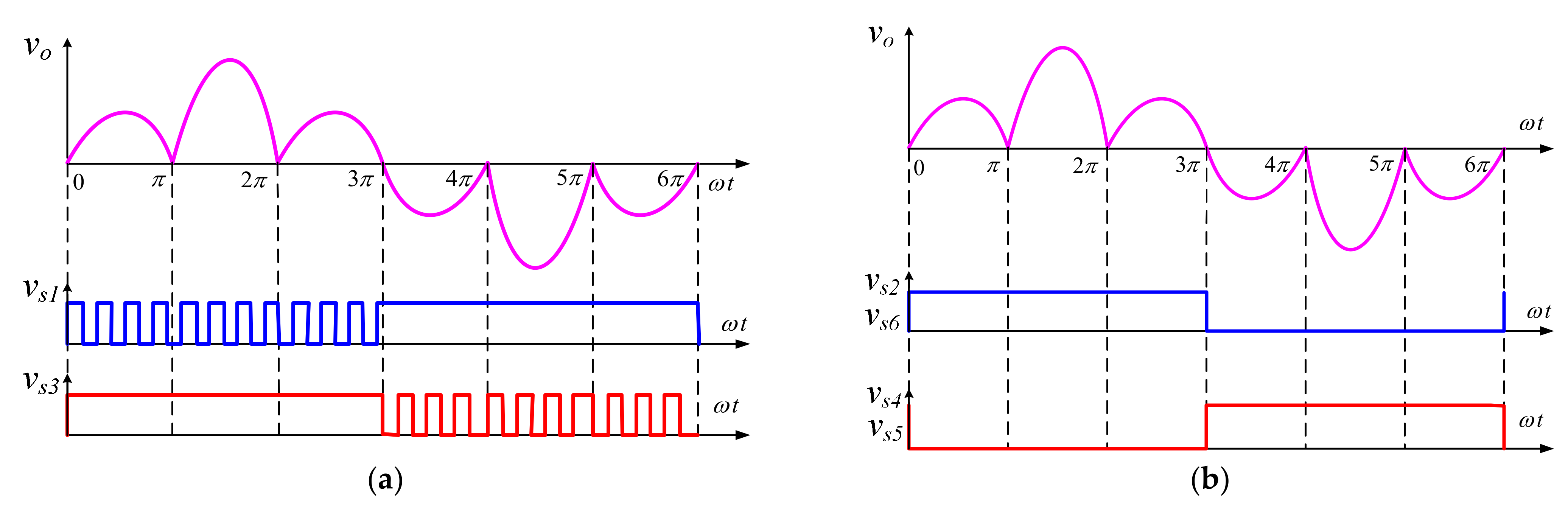
Figure 3b. This action increases the output voltage period three times with respect to the grid’s voltage period. The power quality index of the output voltage is improved by regulating the magnitude of the first and third pulses from the positive pulses and fourth and sixth pulses from the negative pulses of output voltage. A similar approach may be tested for other output frequency requirements.
The operation of the developed circuit is supported with the generated control outputs of Figure 4a,b illustrating how voltage and frequency control is achieved.
The plotted control signals of Figure 4a highlight the voltage control achieved by employing the PWM strategy. This control facilitates the governing of the maximum value of the selected output pulse from zero to the maximum input voltage level. The PWM behavior of the transistor Q1 and Q3 is responsible for governing the desired instantaneous voltage during the positive and negative half cycles of the load voltage. The frequency converter is responsible for output frequency control; this task is attained by arranging the voltage pulses obtained from the voltage controller as viewed from Figure 3a into their non-inverted and inverted forms. The instantaneous load voltage is in-phase with the instantaneous voltage pulses at its input terminal once the transistor Q2 and Q6 operate in conducting states. The turning on the transistors Q4 and Q5 transform positive pulse into negative pulses. The control inputs of Figure 4b are employed to obtain the required output of Figure 3b. The further detail of how the controllable output can be produced is described and highlighted from the power flow loops of Figure 5 and Figure 6.

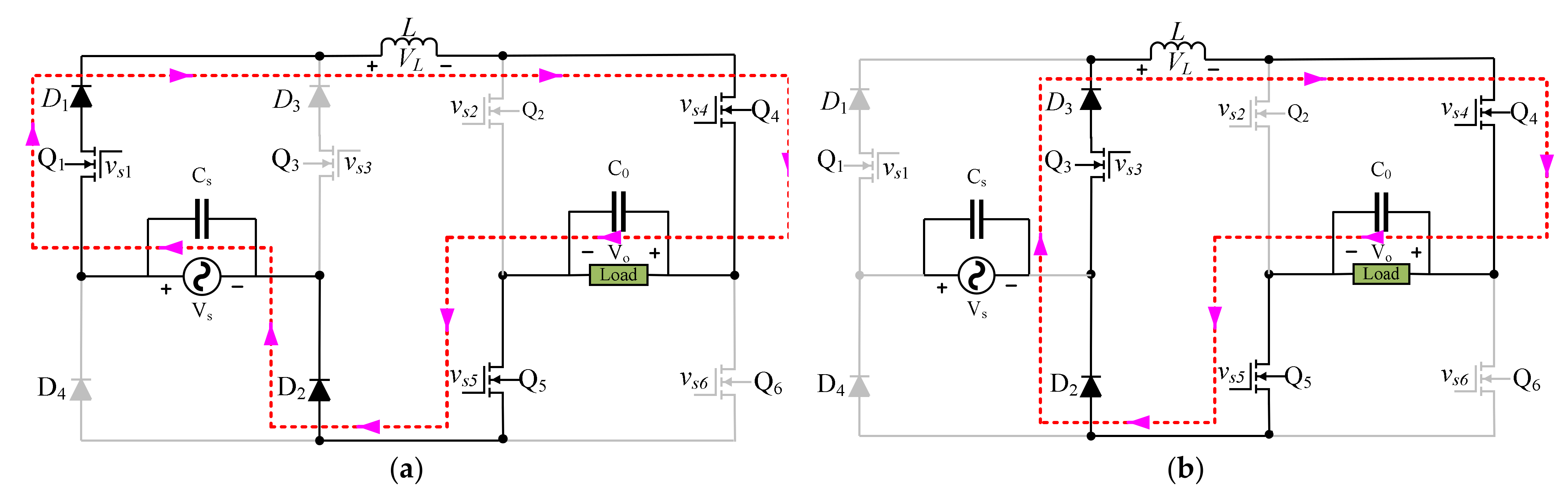
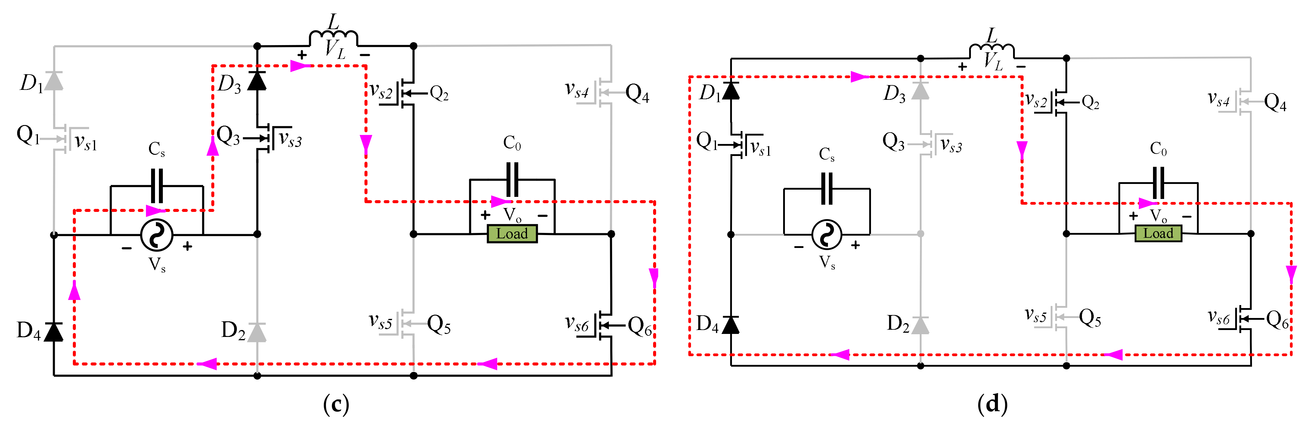
2.1. Operation as an Absolute Value Voltage Controller

It has already been stated that output frequency conversion is linked with the operation of transistors Q2, Q6 and Q4, Q5 to non-invert and invert the voltage available at the input terminals of the frequency controller bridge. The regulated and non-regulated voltage operations depend on the high-frequency switching of the transistors Q1 and Q3. They can regulate the voltage once their operation is controlled in a PWM manner; otherwise, their conduction facilitates the power transfer path from input to output.
The transistor Q1 always operates in voltage control mode or non-voltage control mode only if the input is positive, as it is shown in part ‘a’ of Figure 5 and Figure 6. In voltage control mode, it turns on and turns off at high-frequency to store and transfer the power in the inductor as described in Figure 5a,b and Figure 6a,b. In part ‘a’ of these figures, the power is stored in the inductor (L), and in (b), the stored power is released to load. In this operating mode, the operation of the transistors Q1 and Q3 is complementary, and the role of transistor Q3 is to establish the power transfer path once the transistor Q1 changes it state from on to off. In non-regulated voltage modes, the transistor Q1 only conducts during the positive half cycle of the input voltage as described in power transferring loops in part ‘a’ of Figure 5 and Figure 6.
During the negative half of the line voltage, the voltage regulated and non-regulated capabilities are governed through the operation of transistor Q3. It operates at a high frequency to ensure the voltage control facility by storing the power in the inductor and here the conduction of transistor Q1 helps to release that stored power as described in part ‘c’ and ‘d’ of Figure 5 and Figure 6. In non-regulated voltage mode, as there is no need to store the power in the inductor, only the low-frequency operation of transistor Q3 completes this task, and it can be viewed from the power transferring loops as described in part ‘c’ of Figure 5 and Figure 6.

2.2. Operation as a Frequency Controller

The non-inverted and inverted forms of the output voltage are obtained with the switching of the transistors employed in the frequency controller circuit. There is no change in the operating behavior of the operating transistors employed in the absolute value voltage controller circuit as their role is only to convert the voltage regulated and non-regulated pulses of the input into their absolute form. The control inputs vs2 and vs6 generate the positive output as viewed by highlighted loops of Figure 5a–d for positive and negative input, respectively. Inverted behavior of the output is governed by changing the role of control signal vs2vs6 with vs4vs5. The power transferring paths of Figure 6a,c illustrate how the voltage at the output is inverted. The turning on of the transistors Q4 and Q5 produce the negative output from positive input while the on-state operation of the transistors Q2 and Q6 during negative input convert it to a positive value. The voltage regulation capability of the output is attained by storing and releasing the power in the inductor as may be seen in the power flow loops of Figure 6a–d for a period in which the input is positive and negative respectively. The instantaneous value of the non-inverted output voltage in a voltage-regulated and non-regulated mode is mathematically computed in Equations (1) and (2):
v o ω t = D V m Sin ω t
v o ω t = V m Sin ω t
The instantaneous inverted form of the output voltage during the voltage regulated and non-regulated modes is mathematically formulated in Equations (3) and (4):
v o ω t = D V m Sin ω t π
v o ω t = V m Sin ω t π
Here ‘D’ is the duty cycle of the voltage control circuit, and its value may be governed from 0% to 100% range and ‘Vm’ is the peak value of the input voltage.

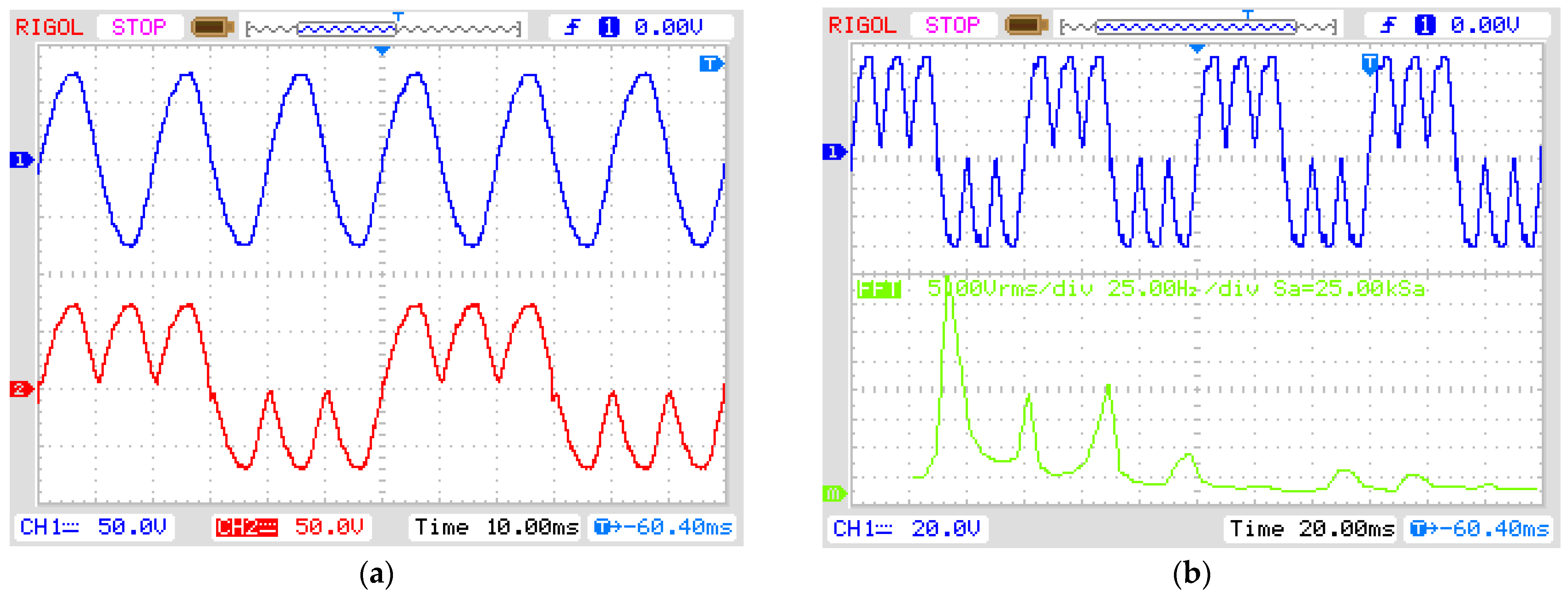
3. Power Quality Analysis of Output Voltage

For this purpose, the decomposition of the output voltage represented in Figure 3b is decomposed into its parent sinusoidal forms in Figure 7. Here the instantaneous value of the output pulse No. 1, 3, 4, and 6 are controllable but the second and fifth pulses have non-regulated voltage capabilities. The instantaneous form of this sort of output voltage waveform or pulses is mathematically described in Equations (5)–(9).
v o ω t = D V m Sin ω t 0 ω t π
v o ω t = V m Sin ω t π ω t 2 π
v o ω t = D V m Sin ω t 2 π ω t 4 π
v o ω t = V m Sin ω t 4 π ω t 5 π
v o ω t = D V m Sin ω t 5 π ω t 6 π
The pulse selective or half-cycle mathematical approach reported in [15] is applied to compute the rms voltage and Fourier coefficients of Equation (10) for the output voltage waveform of Figure 7.
v o ω t = a o + n = 1 a n cos n ω t 3 + b n sin n ω t 3
V o ( r m s ) = 1 2 π 0 π D 2 V m 2 sin 2 ω t d ω t π 2 π V m 2 sin 2 ω t d ω t + 2 π 3 π D 2 V m 2 sin 2 ω t d ω t + 3 π 4 π D 2 V m 2 sin 2 ω t d ω t 4 π 5 π V m 2 sin 2 ω t d ω t + 5 π 6 π D 2 V m 2 sin 2 ω t d ω t
V o ( r m s ) = V m 2 D 2 + 1 6
a o = 1 2 π 0 π D V m sin ω t d ω t π 2 π V m sin ω t d ω t + 2 π 3 π D V m sin ω t d ω t + 3 π 4 π D V m sin ω t d ω t 4 π 5 π V m sin ω t d ω t + 5 π 6 π D V m sin ω t d ω t = 0
a n = 2 2 π 0 π D V m sin ω t cos n ω t 3 d ω t π 2 π V m sin ω t cos n ω t 3 d ω t + 2 π 3 π D V m sin ω t cos n ω t 3 d ω t + 3 π 4 π D V m sin ω t cos n ω t 3 d ω t 4 π 5 π V m sin ω t cos n ω t 3 d ω t + 5 π 6 π D V m sin ω t cos n ω t 3 d ω t = 0
b n = 2 2 π 0 π D V m sin ω t sin n ω t 3 d ω t π 2 π V m sin ω t sin n ω t 3 d ω t + 2 π 3 π D V m sin ω t sin n ω t 3 d ω t + 3 π 4 π D V m sin ω t sin n ω t 3 d ω t 4 π 5 π V m sin ω t sin n ω t 3 d ω t + 5 π 6 π D V m sin ω t sin n ω t 3 d ω t
b n = 0 f o r n = 2 , 4 , 6 , 12 V m 1 + D π n 2 9 sin n π 3 f o r n = 1 , 3 , 5 , 7
For fundamental components (n = 3)
a n n = 3 = 2 2 π 0 π D V m sin ω t cos ω t d ω t π 2 π V m sin ω t cos ω t d ω t + 2 π 3 π D V m sin ω t cos ω t d ω t + 3 π 4 π D V m sin ω t cos ω t d ω t 4 π 5 π V m sin ω t cos ω t d ω t + 5 π 6 π D V m sin ω t cos ω t d ω t = 0
b n n = 3 = 2 2 π 0 π D V m sin ω t sin ω t d ω t π 2 π V m sin ω t sin ω t d ω t + 2 π 3 π D V m sin ω t sin ω t d ω t + 3 π 4 π D V m sin ω t sin ω t d ω t 4 π 5 π V m sin ω t sin ω t d ω t + 5 π 6 π D V m sin ω t sin ω t d ω t
b n n = 3 = 2 D 1 V m 3
The Fourier expression of the output voltage of Equation (10) can be represented in Equation (20) by putting the value of the computed harmonic coefficients ao, an, and bn:
v o ω t = 2 D 1 V m 3 sin ω t + n = 1 , 3 , 5 , 7 , 12 1 + D V m π n 2 9 sin n π 3 sin n ω t 3
The fundamental component of the output voltage waveform is obtained by putting the value of n = 1 in Equation (20):
v o 1 ω t = 3 3 1 + D V m 4 π sin ω t 3
The rms value of this voltage component is obtained as:
v o 1 ω t = 3 3 1 + D V m 4 2 π
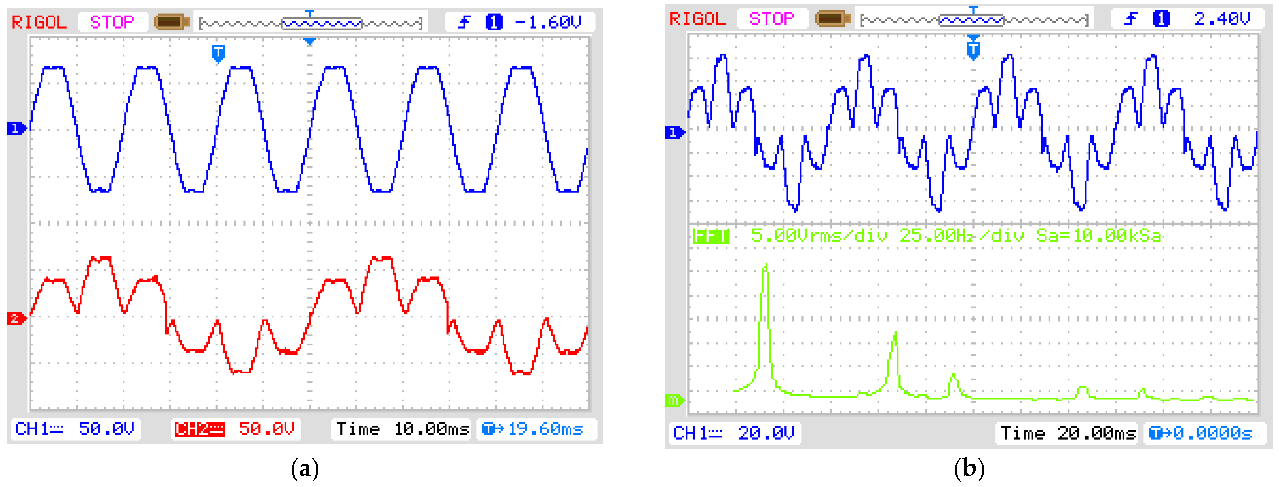
If the duty cycle of the voltage-regulated pulses is set to ‘1’ then the magnitude of all voltage-regulated pulses becomes equal to the magnitude of the non-regulated voltage pulses. The output voltage waveform with this duty cycle is described in Figure 8.
The instantaneous value of the output voltage and voltage fundamental component, total rms voltage may compute by putting the value of duty cycle D = 1 in Equation (20), Equation (21), and Equation (12) respectively:
v o ω t = V m 3 sin ω t + n = 1 , 5 , 7 , 11 , 24 V m π n 2 9 sin n π 3 sin n ω t 3
v o 1 ω t = 3 3 V m 2 π sin ω t 3
V r m s = V m 2 = 0.707 V m
Its rms value, the rms value of the total harmonic components, and THD of the output voltage of Figure 8 may be found as:
V o 1 ( r m s ) = 3 3 V m 2 2 π = 0.5847 V m
V o h ( r m s ) = V o ( r m s ) 2 V o 1 ( r m s ) 2 = 0.3976 V m
T . H . D = V r m s 2 V 01 ( r m s ) 2 V 01 ( r m s ) 2 68 %
The low power quality of the output voltage needs investigation as it has a high value. It is observed from Equation (20) that output harmonic at source voltage frequency can be eliminated by setting the value of the duty ratio or duty cycle to 0.5. The output voltage wave with this duty cycle control may be viewed from Figure 9.
The instantaneous value of the output voltage and voltage fundamental component, total rms voltage may compute by putting the value of duty cycle D = 0.5 in Equation (20), Equation (21), and Equation (12), respectively.
v o ω t = n = 1 , 5 , 7 , 11 , 18 V m π n 2 9 sin n π 3 sin n ω t 3
v o 1 ω t = 9 3 V m 8 π sin ω t 3
V o ( r m s ) = V m 2 = 0.5 V m
Similarly, the rms value, the rms value of the total harmonic components, and THD of the output voltage of Figure 9 may be found as:
V o 1 ( r m s ) = 9 3 V m 8 2 π = 0.43 V m
V o h ( r m s ) = V o ( r m s ) 2 V o 1 ( r m s ) 2 = 0.43 V m
T . H . D = V o ( r m s ) 2 V o 1 ( r m s ) 2 V o 1 ( r m s ) 2 55 %
With this approach, the THD or harmonic factor is lowered from 68% to almost 55%.

4. Comparison with Similar Topologies

The requirement of the output voltage that includes the frequency and voltage regulation is achieved by developing a transformer-less AC-AC converter. This approach has the ability to vary the magnitude of the selected output pulse via the PWM control. The range for the output voltage control lies from 0% to 100% value of the input peak or rms voltage. Such variation in the output pulses governs the required output rms voltage and power quality. The voltage control of the selected pulses via the use of multiple transformer winding requires more space, and this is a costly solution or approach. The application of the low-frequency transformer is the main source of power losses and low conversion efficiency. Although the converter reported in [25] has the ability to achieve the required output with the conduction of one diode and one thyristor during any instant of its operation, but its voltage control capability requires a multiple windings transformer operated at line frequency. The voltage of these windings is connected to the load through the number of diodes and thyristors. The number of voltage levels is proportional to the number of the transformer’s windings. Increasing the number of winding increases the required number of diodes and thyristors as one thyristor and two diodes are associated with each winding.
The AC voltage controllers that have the ability to govern the voltage regulation with PWM control for both the non-inverted and inverted forms of the input voltage at the output may also be employed to achieve such outputs without involving bulky line frequency transformers [26,27]. The proposed circuit is developed with this principle and its implementation uses a fixed number of semiconductor devices. The required voltage level in the output may be obtained just by regulating the duty cycle control of the PWM control. The elimination of the low line frequency transformer saves the required space and cost significantly. The control input signal of the proposed circuit and power converting circuits described in [23,26,27] are drawn in Figure 10. The gate control inputs of the converter reported in [26] are demonstrated in Figure 10b. The peak amplitude of the second and fifth output pulses is equal to the peak of the input and they are the inverted forms of the input voltage. The amplitude of remaining output pulses is one-half of the input peak and their characteristics are non-inverted with respect to the input voltage. Therefore, the required voltage gain is ‘−1’ for the second and fifth output pulses while it is ‘0.5’ for the rest of the pulses. This circuit has the ability to convert the input voltage to a non-inverted voltage buck form with a voltage gain of ‘0.5’. But its output cannot be directly connected with the input source to obtain its inverted form with the voltage gain of ‘−1’. Its voltage inverting form can only be obtained from its buck-boost operation. Therefore, its non-inverted and inverted control is non-identical. This non-symmetrical form of the gate control signals becomes complex for output voltage regulation. The voltage buck-boost operation always increases the peak-to-peak inductor ripple current, and voltage and current rating of the devices. The duty cycle value (k) to obtain the output for voltage buck and buck-boost operation is ‘0.5’. The value of the peak-to-peak ripple ( Δ I L ) inductor current, average inductor current ( I L ), and maximum breakover voltage ( V b o ( m ) ) is computed as:
Δ I L = 0.5 V s ( p ) L T s
I L = I o 1 k = 2 I o
V b o ( m ) = V s ( m ) + V o ( m ) = 2 V s ( m )
In these equations, the ‘Ts’ is the PWM switching period, ‘Io’ is output current, ‘Vo(m)’ and ‘Vs(m)’ are the maximum output and input voltage, respectively. The preceding issues are addressed in the circuit arrangement reported in [23] by ensuring the identical control scheme that is effectively used to obtain the output in non-inverted and inverted form. Its value of maximum breakover voltage, inductor ripple, and average current can be represented as in Equations (38)–(40). These values are low with respect to the circuit described in [26]. Also, the voltage control schemes of this topology as described in Figure 10c are relatively simple than that of the circuit reported in [26]. The major issue in this existing topology is the use of more devices and gate control circuits that are the main sources for the high volume and cost. These issues are addressed in the proposed circuit by reducing the number of switching devices and gate control circuits. Also, its gate control algorithm as depicted in the plot of Figure 10a is much simpler with the same value of maximum breakover voltage, inductor ripple, and average current than that of [26]. This achievement reduces the circuit’s overall volume:
Δ I L = 0.25 V s ( p ) L T s
I L = I o
V b o ( m ) = V s ( m )
The power conversion losses are the other index used to compare the performance of the various circuit topologies. They include the losses caused by the filtering components, switching and conduction losses of the semiconductor devices, and core losses of the line frequency input transformer. The contribution of the losses caused by the filtering com is ignorable as they have a low value of their internal resistance [26]. The switching losses of high switching frequency (fs) operating transistors depend on their rise (tr) and fall time (tf), and for diodes, they are related to their reverse recovery charge (Qrr). These losses also depend on the value of current and voltage at which the switching devices are going to change their operating states ‘on’ to ‘off’ and vice versa. The instantaneous values of the voltage and current may regard constant as their variation can be ignored at high switching frequencies. The value of switching losses for the existing circuits of [23,25,26] and the proposed topology in Equations (41)–(44) respectively may be realized with the procedure as detailed in [28,29].
P s w 1 6 f s V s I o t r + t f + f s V s Q r r
P s w = 0
P s w 1 3 f s V s I o t r + t f + 4 3 f s V s Q r r
P s w 1 6 f s V s I o t r + t f + f s V s Q r r
The value of rise, fall, and reverse recovery times lie in the nanosecond range so, for modern fast switching devices, these losses can be ignored.
The main source of the conversion losses consists of conduction losses (especially for diode and thyristors) and line frequency input transformer. The conduction losses in the topologies reported in [23,25,26] and the developed circuit are calculated from Equations (45)–(48) respectively by following the procedure adopted in [29]. In these equations, the notation Vf is used to represent the value of the forward voltage of a diode or a thyristor. In the same way, the notations Rs and Rf represent the internal resistances of a transistor and a diode or a thyristor, respectively.
P c o n d = 3 I o V f + I o R s + R f
P c o n d = 2 I o V f + I o R f
P c o n d = 4 I o V f + I o R s + R f
P c o n d = 3 I o 2 R s + 2 I o V f + I o R f
The conduction of the developed circuit is less than the topologies in [23,26] and slightly greater than the circuit in [25].
In summary, the comparison Table 1 highlights the significance of the developed circuit topology for one-third of the output frequency.
The proposed circuit is an attractive topology as it has low conversion losses, low value of maximum breakover voltage, low inductor ripple, and average current that lower the voltage and current rating of the operating devices. The proposed circuit also needs a fewer number of semiconductor components without the requirement of the bulky line frequency transformer.

5. Results and Discussion

The computerized and real results are used to prove or validate the strength of the recommended circuit.

5.1. Simulation Results

The Simulink-based system is one of the big sources of modern tools available in the market to analyze the performance of switching converters, so this tool was considered for analysis and verification of the mathematically computed values of the harmonic section. The modeling of the operating devices is carried by considering the parameters of their datasheets. These parameters include the value of internal resistance and voltage drops for their conducting states. The internal on-state resistance of a transistor and diode is set to 100 mΩ and 600 Ω, respectively. The forward drops of the diodes are set to 1 V. A value of load resistance 50 Ω ensures the safe circuit operation to limit the output current to a low value for 65 V input peak. An appropriate value of the required switching frequency of 25 kHz is used to reduce the current and voltage ripple to an acceptable level. The computerized results of Figure 11 describe the frequency control of the output voltage for the ratio of 3 to 1 means output frequency is one-third of the grid frequency. This regulation is achieved without voltage control capability. Hence the peak values of the output positive and negative pulses are equal to input voltage’s peaks (see Figure 11a,b) for the confirmation of these values. The output voltage has a constant rms value that is the same as the input voltage. The FFT plot of Figure 11c confirms the computed value of the output voltage’s THD of Equation (28). Her line frequency harmonic (50 Hz) has significant magnitude, and it is a major cause of the high THD of the output voltage.
The plot of Figure 12b is obtained through Simulink simulation by setting the optimal value of the duty cycle of ‘0.5’ that is investigated in the mathematical results. This duty cycle control sets the peak of the first, third, fourth, and sixth pulse to 50% of the input voltage’s peak. It also leaves the peak value of the output voltage’s second and fifth pulse unchanged. This profile of the peak values of the output voltage’s pulses improves its power quality, and the computed value of the THD of the output voltage in Equation (34) is validated by the plot of Figure 12c.
The FFT plot of Figure 12c demonstrates the significant reduction in the magnitude of the generated at line frequency. This reduction result in low THD of the output voltage.

5.2. Experimental Results

The proposed circuit is practically tested with the development of a lab prototype. The photograph of this practical setup is shown in Figure 13.
It consists of six gate control circuits that are implemented with six hybrid EXB 840 chips and six isolated DC sources that ensure the electrical isolation of the generated control signals. All these control signals are to be aligned with the input AC voltage and for this purpose, one voltage detecting circuit is connected to the input source. The output of this circuit with respect to input AC voltage is shown in Figure 14.
The output of this circuit is approximately 5 V and 0 V during the positive and negative half cycles of the input AC voltage. The output of the voltage sensing circuit is applied to the microcontroller (STM) to generate two high-frequency and four low-frequency gating signals. These six signals are connected to the inputs of the six gate control circuits. The outputs of these gate control circuits as shown in Figure 15 are connected to the input of the six transistors (IRF 840). The plot of Figure 15a shows the generation of one low-frequency signal (red) with respect to input AC voltage (blue). Here it may be observed that the control input used by the output frequency controller is approximately 10 V and 0 V for the first and second half periods of the output voltage, while the plot of Figure 15b depicts the plot of low frequency (blue) and high frequency (red) control signals. The high-frequency signal uses pulse width modulation for a one-half period of the output voltage and it remains logic high (10 V) for the other half period of the output voltage. In the same way, the plots of Figure 15c,d show the control inputs connected to voltage and frequency controller circuits, respectively.
Four abrupt recovery diodes (MUR3040) having high voltage and current ratings are also used to construct the test circuit bench. The voltage and frequency control circuits are separately constructed in the test circuit, and an intermediate inductor with the value of 1 mH facilitates their connection. The inductor not only helps to tackle the shoot-through problem caused by a complementary operated transistor but also acts as an energy-storing element and harmonic filterer. The input and the output capacitor with a value of 4.7 µF are responsible for improving the power quality of both sides of the circuit that is input and output. Input AC voltage with its peak value of 70 V and frequency of 50 Hz is used to test the output without and with the regulation of the output pulses. The output frequency in both cases is 16.667 Hz that is almost one-third of the input frequency. Figure 16a shows the output voltage waveform with respect to the input voltage for the non-regulated output form. The practically obtained FFT of this output is demonstrated in Figure 16b, validating the harmonic profile of the simulated output of Figure 11c.
For the regulated form of the output pulses, the peak value of the output’s first, third, fourth, and sixth pulse is 35 V, while the peak of the second and fifth pulse is 70 V as may be seen from Figure 17a. These amplitudes of the output pulses have optimal values that are addressed in the power quality evaluation section to have a low-value harmonic factor of the output voltage. The plot of Figure 17b depicts that harmonic of 50 Hz frequency in the output is eliminated from the frequency spectrum of the output voltage. This reduction improves the harmonic profile of the output voltage, and as a result, the THD of the output voltage is reduced.

6. Conclusions

This study was focused on the development of an improved direct AC-AC frequency controller having a low value of the THD of the output voltage. Improvement in the power quality is obtained by regulating the peak value of the selected output pulses with the required voltage gain. The optimal value of the voltage gain for the voltage regulating pulses is obtained through the analysis of the power quality. The variation in the output pulses that is based on the use of low-frequency multiple winding transformers is directly linked with the number of windings. Each winding is associated with the requirement of two diodes and one thyristor for the required operation. The number of required semiconductor components increases if the required voltage level of the output pulses is increased. The application of a massive low-frequency transformer with a large number of semiconductor devices is the main source of large size, cost, and overall conversion losses. The adjustment in the output pulses in the proposed circuit topology is achieved by employing the PWM control to the switching devices that eliminate the need for the multiple winding transformer for voltage control. This characteristic fixes the use of a number of the semiconductor devices in the proposed circuit that help to lower the overall volume, conversion losses, and cost. The power quality index of the output voltage is computed with a mathematical approach to confirm the analysis that is based on simulation and practical results.

Author Contributions

Conceptualization, N.A. and G.A.; data curation, G.A. and N.U.; formal analysis, N.A., A.A.A.-A. and M.J.; funding acquisition, N.U. and A.R.Y.; investigation, N.A. and A.B.A.; methodology, G.A. and A.R.Y.; project administration, G.A.; resources, A.A.A.-A. and N.U.; software, M.J. and A.B.A.; validation, M.J. and A.B.A.; writing—original draft, N.A. and G.A.; writing—review and editing, G.A., A.A.A.-A., A.R.Y. and N.U. All authors have read and agreed to the published version of the manuscript.

Funding

This research work is supported by Taif University Researchers Supporting Project number (TURSP-2020/121), Taif University, Taif, Saudi Arabia.

Institutional Review Board Statement

Not applicable.

Informed Consent Statement

Not applicable.

Data Availability Statement

Not applicable.

Acknowledgments

The authors acknowledge the financial support from Taif University Researchers Supporting Project Number (TURSP-2020/121), Taif University, Saudi Arabia. The authors are also thankful to the Department of Electrical Engineering, the University of Lahore, Pakistan for providing the facilities to conduct this research.

Conflicts of Interest

The authors declare no conflict of interest.

References

  1. Nayak, P.; Rajashekara, K.; Pramanick, S.K. Soft-Switched Modulation Technique for a Single-Stage Matrix-Type Isolated DC–AC Converter. IEEE Trans. Ind. Appl. 2018, 55, 7642–7656. [Google Scholar] [CrossRef]
  2. Li, L.; Wu, M.; Wu, S.; Li, J.; Song, K. A Three-Phase to Single-Phase AC-DC-AC Topology Based on Multi-Converter in AC Electric Railway Application. IEEE Access 2019, 7, 111539–111558. [Google Scholar] [CrossRef]
  3. Gomes, R.C.M.; Vitorino, M.A.; Acevedo-Bueno, D.A.; Correa, M.B.D.R. Multiphase Resonant Inverter with Coupled Coils for AC–AC Induction Heating Application. IEEE Trans. Ind. Appl. 2019, 56, 551–560. [Google Scholar] [CrossRef]
  4. Surapaneni, R.K.; Yelaverthi, D.B.; Rathore, A.K. Cycloconverter-Based Double-Ended Microinverter Topologies for Solar Photovoltaic AC Module. IEEE J. Emerg. Sel. Top. Power Electron. 2016, 4, 1354–1361. [Google Scholar] [CrossRef]
  5. Liu, Y.; Sun, Y.; Su, M.; Li, X.; Ning, S. A Single Phase AC/DC/AC Converter with Unified Ripple Power Decoupling. IEEE Trans. Power Electron. 2017, 33, 3204–3217. [Google Scholar] [CrossRef]
  6. De Freitas, N.B.; Jacobina, C.B.; Gehrke, B.S.; Cunha, M.F. Transformer-Based Single-Phase AC–DC–AC Topology for Grid Issues Mitigation. IEEE Trans. Ind. Appl. 2019, 55, 4001–4011. [Google Scholar] [CrossRef]
  7. Felinto, A.S.; Jacobina, C.B.; Fabricio, E.L.L.; de Lacerda, R.P. Six-Leg Three-Phase AC–DC–AC Converter with Shared Legs. IEEE Trans. Ind. Appl. 2021, 57, 5227–5238. [Google Scholar] [CrossRef]
  8. Meng, L.; Shu, Z.; Lei, Y.; Yan, H.; Li, Z.; Ma, L.; Yin, X.; He, X. Optimal Input and Output Power Quality Control of Single-Phase AC–DC–DC Converter with Significant DC-Link Voltage Ripple. IEEE Trans. Ind. Electron. 2019, 67, 10366–10376. [Google Scholar] [CrossRef]
  9. Liu, F.; Ruan, X.; Huang, X.; Qiu, Y.; Jiang, Y. Control Scheme for Reducing Second Harmonic Current in AC–DC–AC Converter System. IEEE Trans. Power Electron. 2021, 37, 2593–2605. [Google Scholar] [CrossRef]
  10. Ashraf, N.; Izhar, T.; Abbas, G.; Awan, A.B.; Farooq, U.; Balas, V.E. A New Single-Phase AC Voltage Converter with Voltage Buck Characteristics for Grid Voltage Compensation. IEEE Access 2020, 8, 48886–48903. [Google Scholar] [CrossRef]
  11. Ahmed, H.F.; Moursi, M.S.E.; Zahawi, B.; Hosani, K.A.; Khan, A.A. Single-Phase Symmetric-Bipolar-Type High-Frequency Isolated Buck-Boost AC–AC Converter with Continuous Input and Output Currents. IEEE Trans. Ind. Appl. 2021, 36, 11579–11592. [Google Scholar] [CrossRef]
  12. Ashraf, N.; Abbas, G.; Ullah, N.; Alkhammash, H.I.; Zubair, M. An Improved Bipolar Voltage Boost AC Voltage Controller with Reduced Switching Transistors. IEEE Access 2021, 9, 90402–90417. [Google Scholar] [CrossRef]
  13. Islam, T.; Fayek, H.H.; Rusu, E.; Rahman, F. Triac Based Novel Single Phase Step-Down Cycloconverter with Reduced THDs for Variable Speed Applications. Appl. Sci. 2021, 11, 8688. [Google Scholar] [CrossRef]
  14. Palavicino, P.C.; Valenzuela, M.A. Robust Estimation and Protection of Locked Charge in Grinding Mills. IEEE Trans. Ind. Appl. 2017, 53, 2608–2620. [Google Scholar] [CrossRef]
  15. Ashraf, N.; Abbas, G.; Abbassi, R.; Jerbi, H. Power Quality Analysis of the Output Voltage of AC Voltage and Frequency Controllers Realized with Various Voltage Control Techniques. Appl. Sci. 2021, 11, 538. [Google Scholar] [CrossRef]
  16. Nguyen, M.K.; Jung, Y.G.; Lim, Y.C.; Kim, Y.M. A Single-Phase Z-Source Buck–Boost Matrix Converter. IEEE Trans. Ind. Appl. 2009, 25, 453–462. [Google Scholar]
  17. Ashraf, N.; Izhar, T.; Abbas, G. A Single-Phase Buck-Boost Matrix Converter with Low Switching Stresses. Math. Probl. Eng. 2019, 2019, 6893546. [Google Scholar] [CrossRef]
  18. Moghaddami, M.; Sarwat, A.I. Single-Phase Soft-Switched AC–AC Matrix Converter with Power Controller for Bidirectional Inductive Power Transfer Systems. IEEE Trans. Ind. Appl. 2018, 54, 3760–3770. [Google Scholar] [CrossRef]
  19. Ahmed, H.F.; Cha, H.; Khan, A.A.; Kim, J.; Cho, J. A Single-Phase Buck–Boost Matrix Converter with Only Six Switches and Without Commutation Problem. IEEE Trans. Power Electron. 2016, 32, 1232–1244. [Google Scholar] [CrossRef]
  20. Ashraf, N.; Izhar, T.; Abbas, G.; Awan, A.B.; Alghamdi, A.S.; Abo-Khalil, A.G.; Sayed, K.; Farooq, U.; Balas, V.E. A New Single-Phase Direct Frequency Controller Having Reduced Switching Count without Zero-Crossing Detector for Induction Heating System. Electronics 2020, 9, 430. [Google Scholar] [CrossRef] [Green Version]
  21. Kumar, A.; Sadhu, P.K.; Mohanta, D.K.; Reddy, M.J.B. An Effective Switching Algorithm for Single Phase Matrix Converter in Induction Heating Applications. Electronics 2018, 7, 149. [Google Scholar] [CrossRef] [Green Version]
  22. Ashraf, N.; Abbas, G.; Ullah, N.; Alahmadi, A.A.; Awan, A.B.; Zubair, M.; Farooq, U. A Simple Two-Stage AC-AC Circuit Topology Employed as High-Frequency Controller for Domestic Induction Heating System. Appl. Sci. 2021, 11, 8325. [Google Scholar] [CrossRef]
  23. Ashraf, N.; Izhar, T.; Abbas, G.; Balas, V.E.; Balas, M.M.; Lin, T.-C.; Asad, M.U.; Farooq, U.; Gu, J. A Single-Phase Buck and Boost AC-to-AC Converter with Bipolar Voltage Gain: Analysis, Design, and Implementation. Energies 2019, 12, 1376. [Google Scholar] [CrossRef] [Green Version]
  24. Mondol, M.H.; Uddin, M.S.; Hossain, E.; Biswas, S.P. A Compact and Cost Efficient Multiconverter for Multipurpose Applications. IEEE Access 2020, 8, 86810–86823. [Google Scholar] [CrossRef]
  25. Uddin, M.; Biswas, S.P.; Islam, M.; Abbas, M.A.; Kouzani, Z.; Mahmud, M.A. A new generalized step-down single-stage AC/AC power converter. Sustainability 2020, 21, 9181. [Google Scholar] [CrossRef]
  26. Ahmed, H.F.; Cha, H.; Khan, A.A.; Kim, H.-G. A Novel Buck–Boost AC–AC Converter with Both Inverting and Noninverting Operations and without Commutation Problem. IEEE Trans. Power Electron. 2015, 31, 4241–4251. [Google Scholar] [CrossRef]
  27. Khan, A.A.; Cha, H.; Ahmed, H.F. High-Efficiency Single-Phase AC–AC Converters without Commutation Problem. IEEE Trans. Power Electron. 2015, 31, 5655–5665. [Google Scholar] [CrossRef]
  28. Bulut, E.B.; Gulbahce, M.O.; Kocabas, D.A. Analysis of a GaN based PWM AC-AC converter with an improved switch loss model. AEU-Int. J. Electron. Commun. 2021, 131, 153578. [Google Scholar] [CrossRef]
  29. Ashraf, N.; Abbas, G.; Ullah, N.; Alzaed, A.N.; Raza, A.; Raza, M.T.; Farooq, U. A New Dual Polarity Direct AC-AC Voltage Regulator Ensuring Voltage Step-Up and Step-Down Capabilities. Appl. Sci. 2021, 11, 11944. [Google Scholar] [CrossRef]
Figure 1. Frequency converter established in [25].
Energies 15 00667 g001
Figure 2. Created circuit’s arrangement.
Energies 15 00667 g002
Figure 3. Expected outputs of (a) absolute value voltage controller and (b) frequency controller.
Energies 15 00667 g003
Figure 4. Control inputs applied to switching transistors of (a) absolute value voltage controller circuit and (b) frequency controller circuit.
Energies 15 00667 g004
Figure 5. Power transferring loops to obtain the non-inverted form at the output with (a,b) positive input value; (c,d) negative input value.
Energies 15 00667 g005
Figure 6. Power transferring loops to obtain the inverted form at the output for (a,b) positive input value; (c,d) negative input value.
Energies 15 00667 g006aEnergies 15 00667 g006b
Figure 7. Decomposition of the output voltage into its parent sinusoidal pulses.
Energies 15 00667 g007
Figure 8. Output voltage waveform with D = 1.
Energies 15 00667 g008
Figure 9. Output voltage waveform with D = 0.5.
Energies 15 00667 g009
Figure 10. Generation of control signals: (a) proposed circuit; (b) circuit in [26]; (c) circuit in [23].
Energies 15 00667 g010
Figure 11. Simulated results of frequency controller without voltage regulation: (a) input voltage; (b) output voltage; (c) FFT of the output voltage.
Energies 15 00667 g011
Figure 12. Simulated results of frequency controller with voltage regulation: (a) Input voltage; (b) output voltage; (c) FFT of the output voltage.
Energies 15 00667 g012
Figure 13. Photograph of practical setup.
Energies 15 00667 g013
Figure 14. Output (red) of voltage sensing circuit with respect to input AC voltage (blue).
Energies 15 00667 g014
Figure 15. Generation of the control signals: (a) low-frequency signal (red) with respect to input AC voltage (blue); (b) high-frequency PWM signal (red) with respect to low frequency signal (blue); (c) high-frequency PWM signals; (d) low- frequency signals.
Energies 15 00667 g015
Figure 16. Real value results of frequency controller without voltage regulation capability: (a) Input (blue) and output (red) voltage; (b) FFT of output voltage pulses.
Energies 15 00667 g016
Figure 17. Real value results of frequency controller with voltage regulation capability: (a) input (blue) and output (red) voltage; (b) FFT of output voltage pulses.
Energies 15 00667 g017
Table 1. Comparison for the output frequency of one-third (3:1) with the respective input frequency.
ParametersSuggested ConverterConverter in [25]Converter in [23]Converter in [26]
Number of transformer windings0400
Number of diodes4886
Number of controlled devices6486
Number of gate supporting circuit6486
Inductor ripple current 0.25 V s ( p ) L T s 0 0.25 V s ( p ) L T s 0.5 V s ( p ) L T s
Inductor average current I o I o I o 2 I o
Maximum breakover voltage V s ( m ) V s ( m ) V s ( m ) 2 V s ( m )
Maximum switching voltage across high-frequency devices 2 V o ( m ) 0 2 V o ( m ) 3 V o ( m )
%THD of the output voltage55555555
Conduction losses 3 I o 2 R s + 2 I o V f + I o R f 2 I o V f + I o R f 3 I o V f + I o R s + R f 4 I o V f + I o R s + R f
Switching losses 1 6 f s V s I o t r + t f + f s V s Q r r 0 1 6 f s V s I o t r + t f + f s V s Q r r 1 3 f s V s I o t r + t f + 4 3 f s V s Q r r
Publisher’s Note: MDPI stays neutral with regard to jurisdictional claims in published maps and institutional affiliations.

