Abstract
This elaboration presents the concept of the design, parameters, experimental investigation, and thermal numerical model solved using the finite element method of a high-power-density DC–DC converter. The analyzed unit can be utilized as a stand-alone converter or as a module for a scalable high-voltage gain system. The converter has a decreased bill of materials since it does not use typical chokes and heatsinks. It is based on switched capacitor circuits supported by a resonant choke which protects against inrush currents. A printed circuit board is utilized not only for the resonant inductance design but also for cooling transistor and diode devices. The paper demonstrates the design concept and the achieved parameters. Experimental results show heat distribution on the printed circuit board and components in a steady state and dynamical states as well. The converter parameters and their efficiency are measured as well. The convergence of experimental results and heating simulations is demonstrated. The numerical model is used for the investigation of design cases. The printed circuit board size, thermal via pattern, and heating process during the overload of the converter are investigated.
1. Introduction
A decrease in the number of components of a power converter is an important optimization issue. Some types of converters and design approaches allow the removal of chokes and heatsinks from a bill of materials (BOM). Such an approach is demonstrated in the presented implementation of the switched capacitor (SC) resonant DC–DC step-up converter. Implementations of the switched capacitor technique for power electronic conversion have been developed significantly in recent years [1]. It is one of the important methods of voltage boosting [2]. Energy transfer in SC converters is achieved with the utilization of periodically recharged capacitors in series-parallel configurations forced by semiconductor switch operation. To avoid inrush currents in SC power converters, the switched capacitor recharging may occur in resonant circuits upon application of low-volume inductors. Oscillatory currents allow operation in zero current switching (ZCS) mode and improve the efficiency of a converter since the converter utilizes resonant inductances which store a very little amount of energy and can be designed as ferrite-less device. Publication [3] presents that the high power density of a switch-mode converter can be achieved by the application of switched capacitor (SC) conversion technique and magnetic-less design. In the case of SC-based converters, a design concept is one of the important optimization problems. In [4], two design concepts were demonstrated for the implementation of converters with a 4-fold voltage step-down ratio. The basic parameters for optimization are the converter power density and efficiency. Design aspects of a novel concept of an SC-based converter for data center applications are presented in [5] where such parameters as efficiency and power density are optimized. The publication [6] presents an SC converter for data center application as well; in its design, the balance between efficiency and the prospective cost is demonstrated. The concept of the resonant SC converter presented in [7] shows its outstanding power density along with high efficiency as well. An analysis of the volume of the passive components is an important design problem that is presented for the resonant SC converter in [8].
The SC voltage doubler belongs also to a family of resonant switched capacitor converters. This is a very effective converter that allows high efficiency and low volume to be achieved. In [9,10], the high efficiency of such a converter was demonstrated with a peak value significantly above 99%. The high efficiency of such a converter was achieved by application of GaN switches, zero voltage switching (ZVS) operation, and power loss minimization in other converter components. The experimental GaN-based setup presented in [10] is characterized by low volume, achieved by the implementation of a planar choke. In [10,11], it was demonstrated that the SC voltage doubler can be used as a module section in a cascaded converter which gives a very effective high voltage gain DC–DC converter. All the components of the converter and the overall design are focused on high power density in a steady state and dynamic states as well.
One of the methods for BOM reduction is heatsinkless design. To avoid significant power limitation, a high temperature of converter operation may be assumed. This requires the use of components with increased rated temperature. An analysis of the high-temperature design concept of the power converter is also an important subject of research and publications [12,13,14,15]. Assuming the operation of a converter and transistors at high temperatures, silicon carbide (SiC) switches were selected in the design concept demonstrated in this paper. In experiments, a high-temperature PCB and capacitors were used as well. Furthermore, no additional heatsink is used, and the PCB board is utilized for heat spread from semiconductor devices. The major research issue demonstrated in this paper is associated with the analysis of thermal parameters of the converter in such a specific design along with its electrical parameters. The power limit, converter volume and dimensions, and heating process can be further compared to other design approaches. The experimental results of the efficiency show a very low drop at larger power and high temperature. Operation at such a high temperature may lead to a decrease in the reliability of the converter; therefore, the proposed design may be considered in a mission profile with a short average time of operation.
Recently, numerical modeling has been developed in the field of modeling and optimization of electronic devices [16,17,18]. Typically, commercial software such as ANSYS (Manufacturer: Canonsburg, PA, USA) and COMSOL (Manufacturer: Burlington, MA, USA) is used to solve problems. The features of such an approach are the possibility of the study of physical phenomena with the geometry and materials applied. Finite element method (FEM)-based modeling is one of the methods for thermal process simulation in power converters. It can be used for a more advanced analysis than the commonly used estimation based on a thermal impedance model. Such a model requires determining parameters such as thermal resistances and capacitances. The literature [16,17] presents examples of modeling methods and their utilization for the thermal design improvement of a PCB-assembled converter. FEM-based thermal 3D modeling of a power converter and its utilization for analysis of the converter’s design is presented in [18]. The presented optimization method in [18] leads to a decrease in the volume of the DC–DC converter.
The paper demonstrates the numerical model computed by the finite element method. The results of the simulations are compared with the experimental results. The model allows for optimization of the design for various purposes. A description of the numerical models, the comparative results with the experiments, and the simulation tests of overload conditions or thermal parameters of the redesigned converter are presented in this paper.
To achieve a low-BOM design the power electronic module based on SC voltage doubler topology has the following features:
- High temperature of operation;
- Heatsinkless design;
- Integrated inductive component;
- Stray capacitance utilized in the energy conversion process;
- Minimum mechanical parts.
Such qualities as high power, high power density, and low volume are beneficial in the proposed design as well. The major contribution of the research is the following:
- Design concept towards high volume and integration of passive components;
- Temperature variation results and steady-state results;
- Determination of a junction of ambient thermal resistance for transistors in the proposed design;
- Determination of the power density of the designed module;
- Demonstration of the efficiency of the DC–DC module and its voltage gain as a function of the temperature of components;
- FEM model implementation for multiphysics simulation of thermal processes in the investigated converter;
- Demonstration of convergence between the FEM model results and experiments;
- Demonstration of optimization cases of the design on the basis of FEM modeling;
- Determination of the relationships between the mechanical and electrical parameters of the system, such as power density vs. PCB size and thermal via pattern.
The paper is organized as follows: Section 2 demonstrates the operation principle of the SC doubler. Section 3 contains the results of the converter efficiency analysis supported by simulation results. Section 4 presents a laboratory setup with efficiency. Section 5 includes FEM model synthesis with a comparison to measured data. Section 6 presents the possibilities of using simulations and PCB optimization. Section 7 concludes the article and includes the proposed topics for future research.
2. Topology of the Power Electronic Module
The converter, which is designed as a power electronic DC–DC boost type, utilizes a topology of a switched capacitor (SC) resonant voltage doubler (Figure 1a). In a unidirectional design, the SCVD is composed of two switches, two diodes, the switched capacitor, and the resonant choke [14]. The principle of operation assumes complementary switching of transistors and transfers the energy in two cycles from the input to the output (Figure 1b,c).
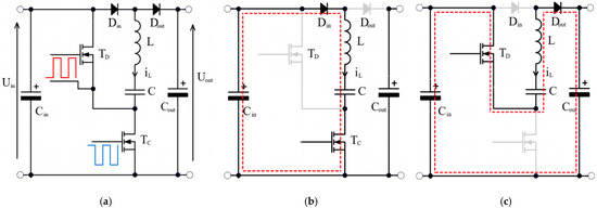
Figure 1.
The power electronic unit: (a) unidirectional SC resonant voltage doubler. Stages of operation of the SCVD: (b) charging and (c) discharging of resonant capacitor.
In a synchronous design, the SCVD can operate bi-directionally or with continuous output voltage control. These concepts of operation of the SCVD are described in detail in [9,10,14]. Basic waveforms which demonstrate the principle of the SCVD operation are presented in Figure 2 [14]. The recharge of the switched capacitor and the oscillatory character of its current are clearly visible.
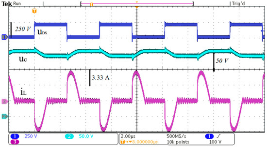
Figure 2.
Experimental steady-state waveforms [14] at Pout = 700 W of the MOSFET drain-source voltage (CH1) and the switched capacitor voltage and current (CH2, CH3).
For Pout = 700 W, the pulsed current of transistors achieves a maximum IDmax ≈ 6 A; in the case of diodes, IDmax = 8 A. The maximum voltage stresses are VSmax ≈ 270 V (with voltage overshoot). To operate in a safe operation area (SOA), the tests were performed to the limit of the case temperature of MOSFET transistors to TCmax = 180 °C.
3. Converter Loss Estimation
The efficiency model of the proposed converter is derived based on conduction losses related to RMS and average currents, which flow through components of the converter as well as through PCB tracks. Switching losses associated with Coss capacitance were also considered.
When analyzing waveforms captured during the simulation research (Figure 3), equal peak current values (Im) can be observed in all considered converter branches. This property allows simplifying further calculations. RMS and average current values can be derived based on the maximal current value, which is bounded to the output power of the converter by the following equation:
where TSW is the switching period and TOSC is the oscillating period dependent on LC component values and can be calculated as follows:
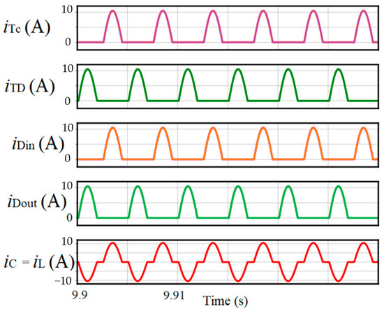
Figure 3.
Current waveforms captured during simulation research performed on the proposed converter.
For further simplifications, it was assumed that the examined converter operates in a steady state with the ideal voltage gain (GU ≈ 2). All fluctuations in the converter’s output voltage were neglected. Once the value Im is derived, the RMS current as well as the average current value of each crucial current path can be calculated using Equations (3)–(6). Those equations were created based on current waveforms captured during the simulation research (recorded waveforms can be seen in Figure 4).
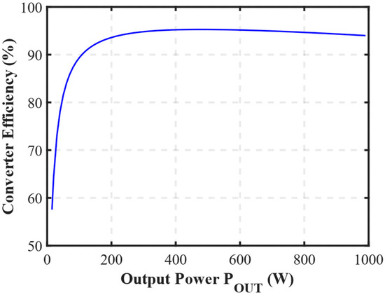
Figure 4.
Efficiency curve of the proposed converter drawn based on the derived analytical model.
Total conduction losses present in the proposed converter are described by the following formula:
The derived efficiency model considers switching losses as well. This type of loss, for this converter, is mainly related to the transistor’s output capacitance (COSS) and remains in direct proportion to the applied switching frequency (fSW):
where is the transistor’s turn-on switching energy.
In this case, switching losses related to transistor turn-off transitions are neglected. This simplification is done assuming that the examined converter operates in a zero current switching mode (Figure 3). A profound analysis of conduction losses in an SC voltage multiplier is presented in [19], and a detailed description of a method utilized for switching loss estimation is provided in [20]. Finally, the converter’s efficiency can be calculated by the following relationship:
The dependency of the converter’s efficiency versus power, based on the derived efficiency model, is presented in Figure 4.
4. Design Concept of the Module
The design assumes the implementation of a 700 W low-volume converter (module) as a base for its further optimization in the FEM simulation environment. Table 1 presents assumptions for the design and concept of an implemented solution. The SCVM converter designed according to the basic concepts and the parameters of the experimental setup are presented in Table 2. The results of efficiency versus the output power measured in the tested design are presented in Figure 5. The converter achieves above 95% peak efficiency, and a very insignificant loss increase for higher output power is observed. Operation at a high temperature changes the efficiency and voltage gain of the converter very insignificantly, which is presented in Figure 6. The tests were performed in a very wide temperature variation (25–180 °C), which proves that the design is appropriate for high-temperature operation. An increase in the temperature affects the resistive loss rise, but conduction losses on diodes fall.

Table 1.
Assumptions and concept of solution of the designed module.
Table 2.
Parameters of the experimental setup and its implementation.
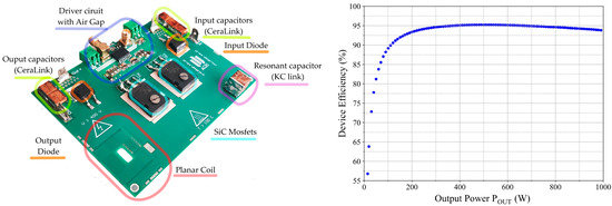
Figure 5.
Power module and experimental results of efficiency versus output power for 50% of duty cycle and fixed frequency fSW.
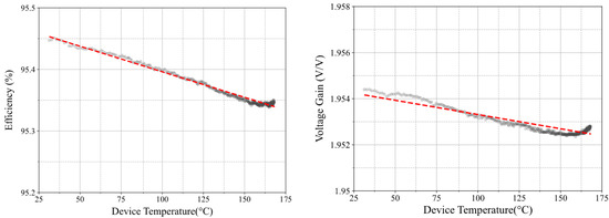
Figure 6.
Experimental results of efficiency and voltage gain vs. temperature (the test performed at Pout = 700 W). The measured data (marked on grey) were approximated with first order polynomial (marked od dashed-red line).
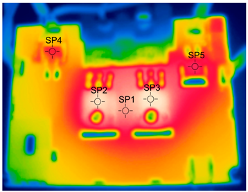
Table 3 presents the board with the selected test points in a steady-state operation with maximum power Pout = 700 W. The power density factor is 4.18 W/cm3. The transistors generate the majority of heat in the system and reach the highest temperature (up to 180.9 °C) whilst diodes and the air choke are not overheated. The design allows collecting the heat from the semiconductor switches to the PCB board.
Table 3.
The temperature of measurement points and results for Pout = 700 W.
The results of temperature in the transient processes (Figure 7) allow the estimation of a thermal impedance curve from the proportion of T(t) and the power of the dissipation process. The temperature of the SP1 test point (Table 3) was taken for the calculation of the heat transfer from the board to the ambient at a given point according to the relationship, assuming that Ploss = 35 W was the total power dissipated in the board:
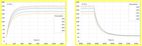
Figure 7.
Experimental results of the temperature measurement in test points SP1–SP5 with the constant load Pout = 700 W. Heating and cooling phases.
For the analysis of energy accumulation, the model of the thermal impedance of the system is important. Figure 8 presents the variation of the thermal impedance versus time, during the heating process, expressed as the Formula (1). From the results, it follows that the heat accumulation (related to thermal capacitance dE/dT) remains approximately in the range of 0.8–0.1 through 10 s.
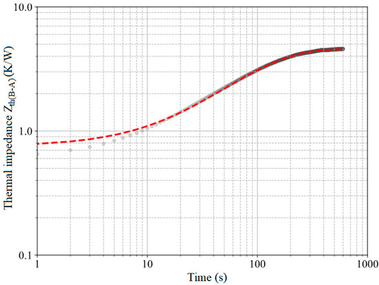
Figure 8.
Experimental results of the thermal impedance ZthB-A at the SP1 test point for Pout = 700 W. The measured data (marked on grey) were approximated with first order polynomial (marked od dashed-red line).
5. Modeling
The simulation model was implemented in the COMSOL Multiphysics software. Two approaches were considered initially. The first, based on the exported geometry from ALTIUM Designer software (Manufacturer: San Diego, CA, USA), failed due to the enormous number of geometrical components which resulted in an enormous mesh size. The second one is based on custom modeling. To minimize the computational effort and open a possibility of custom meshing, the second method was chosen. To obtain the responsible model of the PCB, custom parts were drawn and composed together. Moreover, the parametrized components (such as vias and layers) allowed cloning the parts and modifying their size and locations. The information defining the copper fields in the form of polygon vertex coordinates and a list of vias described by center coordinates, inner and outer diameter, and a list of layers that are connected by individual vias were exported from the PCB package. Finally, a custom PCB generator was realized. For the defined domains, the appropriate material properties were applied and the physics was defined. The basic parameters of the simulation model are described in Table 4. Figure 9 presents the fragment of the developed model with the grid distribution in the cross-section of the board as well as the thermal transient simulation. The thermal measurement points of the PCB during simulation are according to the case presented in Table 3. Since the copper and the dielectric layers are meshed on the inside as well, the thickness of the layers affects the thermal capacity of the board and the heating time-constant.
Table 4.
The material properties used in the simulation model.
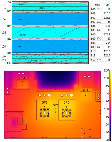
Figure 9.
The developed model with grid distribution—the cross-section view of layers (L) and the thermal transient simulation for Pout = 700 W (a top side view).
Figure 10 presents a comparison of simulation and experimental results of temperature across the converter’s board. The accuracy of heating process simulation at a transient state is the highest for SP1 and equals 6.65%. The accuracy of the model in a steady state is satisfactory. The steady-state relative error for SP1 is 2.75% and for SP2 is 2.61%.
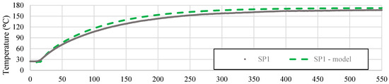
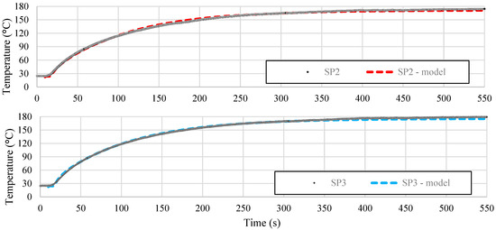
Figure 10.
The simulation results converge to the experimental ones—PCB test points SP1–SP3 for the output power Pout = 700 W.
6. Design Concept Change—The Physical Model Simulation
The physical model of the converter allows performing effective research on redesigned objects under various conditions. In this section, such cases as the temporary overload of the converter, the size of the board, and the thermal design pattern will be investigated.
6.1. Overload of the Converter and the Thermal Effect
Figure 11 presents the temperature rise after the start of the converter with the maximum operating power and under overloaded conditions. The overload allows operating for a limited time interval until the temperature of the device reaches its maximum. For the overload conditions where the power increases to 190% of the rated maximum, the time of safe operation of the device is approximately 67 s. For a short-time (42 s) operation profile, the converter power density can reach a very high value, e.g., 7.964 W/cm3.
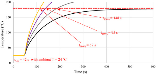
Figure 11.
Power increase vs. time to reach 180 °C in a hot spot of the device. COMSOL Multiphysics simulation results.
6.2. Via Pattern
Heat transfer from the transistors is supported by thermal vias. The pattern of the vias is presented in Figure 12. The original via pattern is composed of 40 open vias with 1.27 mm diameter and 0.71 mm hole size. The vias allow for heat transfer to the bottom side and to all the internal copper layers as well to achieve heat accumulation. Forty thermal vias fill nearly all the available space around the thermal pad, but the number of vias may be optimized. A large mechanical pad is used as a thermal pad as well which supports the vias.
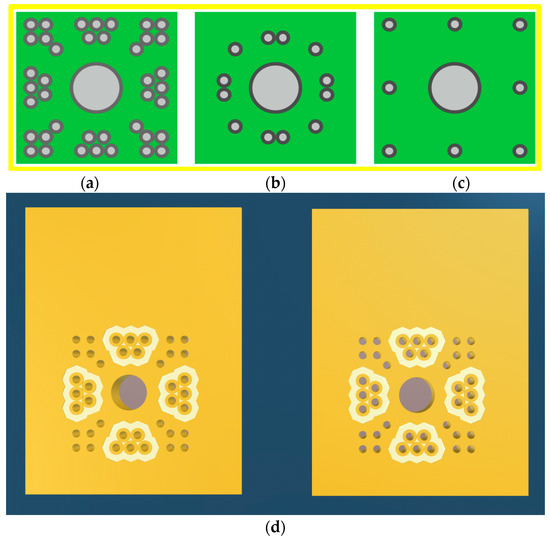
Figure 12.
The transistors’ thermal via pattern in the model of the board PCB: (a) all vias—equivalent to the experimental setup; (b) reduced model with 12 vias; (c) model with 8 vias; (d) design for experimental tests (in ALTIUM Designer software—3D perspective).
The realized model is flexible in the configuration of components, including vias. On the basis of proposed locations, they were distributed below the transistor pad with a specific custom distribution. In the performed simulation tests, the number of vias around a transistor was decreased and a temperature steady-state value was computed (Figure 13). From the results presented in Figure 13, it is seen that the use of 40 vias allows decreasing the steady state temperature by 6 °C when compared to the case where 8 vias were used. This allows achieving cost reduction when such a range of temperature increase is acceptable.
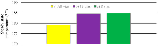
Figure 13.
The temperature change process after the start of the converter with the power of 700 W. Simulation of the cases with 40, 12, and 8 thermal vias.
6.3. Extended Board Size Simulation Analysis of the Board Extending
Numerical simulations allow the effective evaluation of the board geometry change. In the performed tests, the analyzed PCB was extended in one direction (Figure 14) to increase all the copper layers and improve the board’s cooling and heat accumulation. From the results presented in Figure 14 and Figure 15, it is seen that an increase in the PCB area by 5600 mm2 allows a reduction in the steady state temperature by approximately 5 degrees.
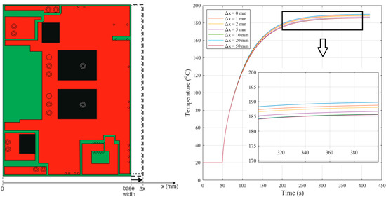
Figure 14.
The regular PCB geometry with marked extension. Temperature transient of the hotspot (SP3) for different board sizes.
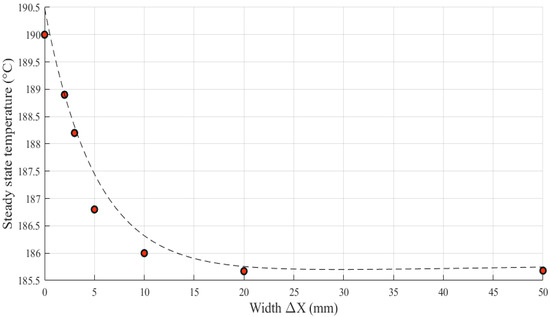
Figure 15.
The regular PCB geometry with marked extension. Temperature transient of the hotspot (SP3) for different board sizes.
The converter with an increased board size may be designed to operate with a higher power. An insignificant impact on the time constant of the heating process is observed. The time constant value changes are below 1 s. Furthermore, no significant impact of maximal temperature after 20 mm of extension is visible.
7. Conclusions
The problems of the power electronic converter design optimization supported by multiphysics simulations are presented. Starting from the base, the parameters of the converter can be optimized in the simulation model. The experimental results of the 700 W SC DC–DC step-up converter and its equivalent simulation model were presented. The experimental results show the power losses, the efficiency of the converter, the design concept, and the heat distribution over the components. The efficiency of the analyzed converter in the tested design decreased insignificantly in a wide range of power and temperature changes. The presented design is heatsinkless. Heat is spread from the PCB surfaces. Despite its very low weight, the converter has the ability of heat accumulation and can work overloaded for a limited time interval. The design verification was performed by custom model and numerical simulation which allows the demonstration of such problems as the overload of the converter and the optimization of the thermal via count and the PCB cooling ability. Heat accumulation was also observed in the simulation results. The converter can remain operating with nearly 200% overload for approximately one minute until the maximal temperature is achieved. Simulation results also show that an adequate increase in thermal via number allows limiting the transistor’s solder point temperature significantly. An increase in the PCB dimensions brings a temperature decrease in a limited range. The relationship is nonlinear and shows the initial positive effect only. The presented results can be further enhanced for converter design and optimization of the parameters.
Author Contributions
Conceptualization, R.S., M.C., A.P. and M.S.; Data curation, R.S., A.P., M.S. and S.F.; Formal analysis, R.S. and M.C.; Funding acquisition, R.S.; Investigation, M.S., A.P., M.C. and S.F.; Methodology, R.S., A.P., M.C. and M.S.; Project administration, R.S. and A.P.; Resources, R.S., M.C. and A.P.; Software, A.P., M.S. and M.C.; Supervision, R.S., A.P. and M.S.; Visualization, A.P., M.C., R.S. and S.F.; Writing—original draft, R.S., M.C. and S.F.; Writing—review & editing, R.S., M.C. and A.P. All authors have read and agreed to the published version of the manuscript.
Funding
This research received no external funding.
Institutional Review Board Statement
Not applicable.
Informed Consent Statement
Not applicable.
Data Availability Statement
Not applicable.
Conflicts of Interest
The authors declare no conflict of interest.
References
- De Souza, A.F.; Tofoli, F.L.; Ribeiro, E.R. Switched Capacitor DC-DC Converters: A Survey on the Main Topologies, Design Characteristics, and Applications. Energies 2021, 14, 2231. [Google Scholar] [CrossRef]
- Forouzesh, M.; Siwakoti, Y.P.; Gorji, S.A.; Blaabjerg, F.; Lehman, B. Step-Up DC–DC Converters: A Comprehensive Review of Voltage-Boosting Techniques, Topologies, and Applications. IEEE Trans. Power Electron. 2017, 32, 9143–9178. [Google Scholar] [CrossRef]
- Cheong, S.V.; Chung, H.; Ioinovici, A. Inductorless DC-to-DC converter with high power density. IEEE Trans. Ind. Electron. 1994, 41, 208–215. [Google Scholar] [CrossRef]
- Lyu, X.; Li, Y.; Ren, N.; Jiang, S.; Cao, D. A Comparative Study of Switched-Tank Converter and Cascaded Voltage Divider for 48-V Data Center Application. IEEE J. Emerg. Sel. Top. Power Electron. 2020, 8, 1547–1559. [Google Scholar] [CrossRef]
- Li, Y.; Lyu, X.; Cao, D.; Jiang, S.; Nan, C. A 98.55% Efficiency Switched-Tank Converter for Data Center Application. IEEE Trans. Ind. Appl. 2018, 54, 6205–6222. [Google Scholar] [CrossRef]
- Tahir, R. Novel Switched-Capacitor Converter Supports 48-V Power Architecture In Data Centers, 2019 How2Power. Available online: https://www.infineon.com/dgdl/Infineon-DCDC_48V_Power_Architecture_H2PToday-Article-v01_00-EN.pdf?fileId=5546d4626d66c2b1016d6af0758558cb (accessed on 12 July 2022).
- Ye, Z.; Lei, Y.; Pilawa-Podgurski, R.C.N. The Cascaded Resonant Converter: A Hybrid Switched-Capacitor Topology With High Power Density and Efficiency. IEEE Trans. Power Electron. 2020, 35, 4946–4958. [Google Scholar] [CrossRef]
- Ye, Z.; Sanders, S.R.; Pilawa-Podgurski, R.C.N. Modeling and Comparison of Passive Component Volume of Hybrid Resonant Switched-Capacitor Converters. IEEE Trans. Power Electron. 2022, 37, 10903–10919. [Google Scholar] [CrossRef]
- Vasić, M.; Serrano, D.; Toral, V.; Alou, P.; Oliver, J.A.; Cobos, J.A. Ultraefficient Voltage Doubler Based on a GaN Resonant Switched-Capacitor Converter. IEEE J. Emerg. Sel. Top. Power Electron. 2019, 7, 622–635. [Google Scholar] [CrossRef]
- Waradzyn, Z.; Stala, R.; Mondzik, A.; Skała, A.; Penczek, A. GaN-Based DC-DC Resonant Boost Converter with Very High Efficiency and Voltage Gain Control. Energies 2020, 13, 6403. [Google Scholar] [CrossRef]
- Piróg, S.; Stala, R. DC–DC boost converter with high voltage gain and a low number of switches in multisection switched capacitor topology. Arch. Electr. Eng. 2018, 67, 617–627. [Google Scholar] [CrossRef]
- Buttay, C.; Planson, D.; Allard, B.; Bergogne, D.; Bevilacqua, P.; Joubert, C.; Lazar, M.; Martin, C.; Morel, H.; Tournier, D.; et al. State of the art of high temperature power electronics. Mater. Sci. Eng. B 2011, 176, 283–288, ISSN 0921-5107. [Google Scholar] [CrossRef]
- Zhong, X.; Wu, X.; Zhou, W.; Sheng, K. An All-SiC High-Frequency Boost DC–DC Converter Operating at 320 °C Junction Temperature. IEEE Trans. Power Electron. 2014, 29, 5091–5096. [Google Scholar] [CrossRef]
- Chojowski, M.; Stala, R.; Piłat, A.; Skowron, M.; Folmer, S. The Design Concept Of Low Cost And Volume Switched-capacitor DC-DC Resonant Converter. In Proceedings of the 2021 IEEE 19th International Power Electronics and Motion Control Conference (PEMC), Gliwice, Poland, 25–29 April 2021; pp. 200–206. [Google Scholar] [CrossRef]
- Cui, M.; Sun, R.; Bu, Q.; Liu, W.; Wen, H.; Li, A.; Liang, Y.C.; Zhao, C. Monolithic GaN Half-Bridge Stages With Integrated Gate Drivers for High Temperature DC-DC Buck Converters. IEEE Access 2019, 7, 184375–184384. [Google Scholar] [CrossRef]
- de Jong, E.C.W.; Ferreira, J.A.; Bauer, P. Thermal design based on surface temperature mapping. IEEE Power Electron. Lett. 2005, 3, 125–129. [Google Scholar] [CrossRef]
- Lee, S.-Y.; Pfaelzer, A.G.; van Wyk, J.D. Comparison of Different Designs of a 42-V/14-V DC/DC Converter Regarding Losses and Thermal Aspects. IEEE Trans. Ind. Appl. 2007, 43, 520–530. [Google Scholar] [CrossRef]
- Kim, N.; Han, C. Thermal analysis and design of a 75-W hybrid-type DC–DC converter for space applications. Microelectron. Reliab. 2014, 54, 1555–1561. [Google Scholar] [CrossRef]
- Waradzyn, Z.; Stala, R.; Mondzik, A.; Penczek, A.; Skala, A.; Pirog, S. Efficiency analysis of MOSFET-based air-choke resonant DC–DC step-up switched-capacitor voltage multipliers. IEEE Trans. Ind. Electron. 2017, 64, 8728–8738. [Google Scholar] [CrossRef]
- Kazimierczuk, M.K.; Czarkowski, D. Resonant Power Converters, 2nd ed.; Wiley: Hoboken, NJ, USA, 2011. [Google Scholar]
Publisher’s Note: MDPI stays neutral with regard to jurisdictional claims in published maps and institutional affiliations. |
© 2022 by the authors. Licensee MDPI, Basel, Switzerland. This article is an open access article distributed under the terms and conditions of the Creative Commons Attribution (CC BY) license (https://creativecommons.org/licenses/by/4.0/).