
A Novel Overlap-Time Effect Suppression for Current Source Converter


Abstract
:1. Introduction
- (1)
- The effect of overlap time on grid current under the non-nearest three-vector synthesis reference vector scheme is analyzed, and the relationship is derived between the overlap time and the introduced harmonics in grid current.
- (2)
- A novel overlap-time suppression method is proposed, that is, constructing a freewheeling channel by controlling specific switch (Freewheeling switch) to maintain conduction, thus ensuring the continuity of the DC-side inductor current, so that the proposed scheme does not need to incorporate overlap time.
- (3)
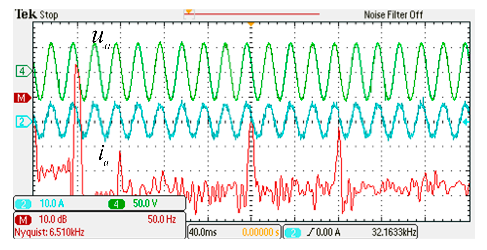
- The experimental results obtained when the laboratory demonstrator uses a power of 200 W and the simulation results verify the correctness of the theoretical analysis and the effectiveness of the proposed overlap-time effect mitigation scheme.
2. Related Work
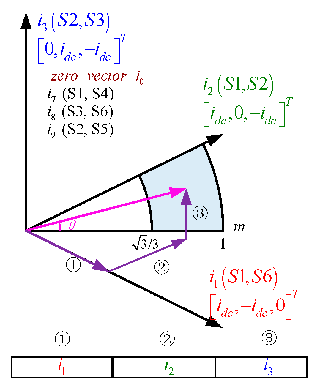
2.1. Operation Mechanism for Non-Nearest Three Vectors Scheme
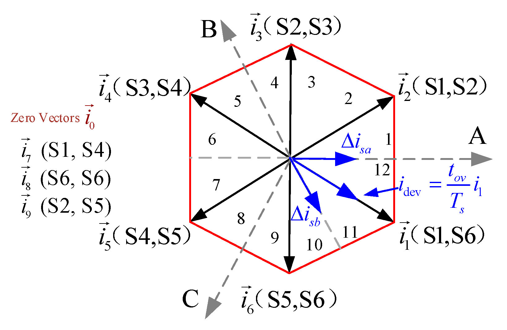
2.2. Effect of Overlap Time with Non-Nearest Three Vectors Modulation Scheme
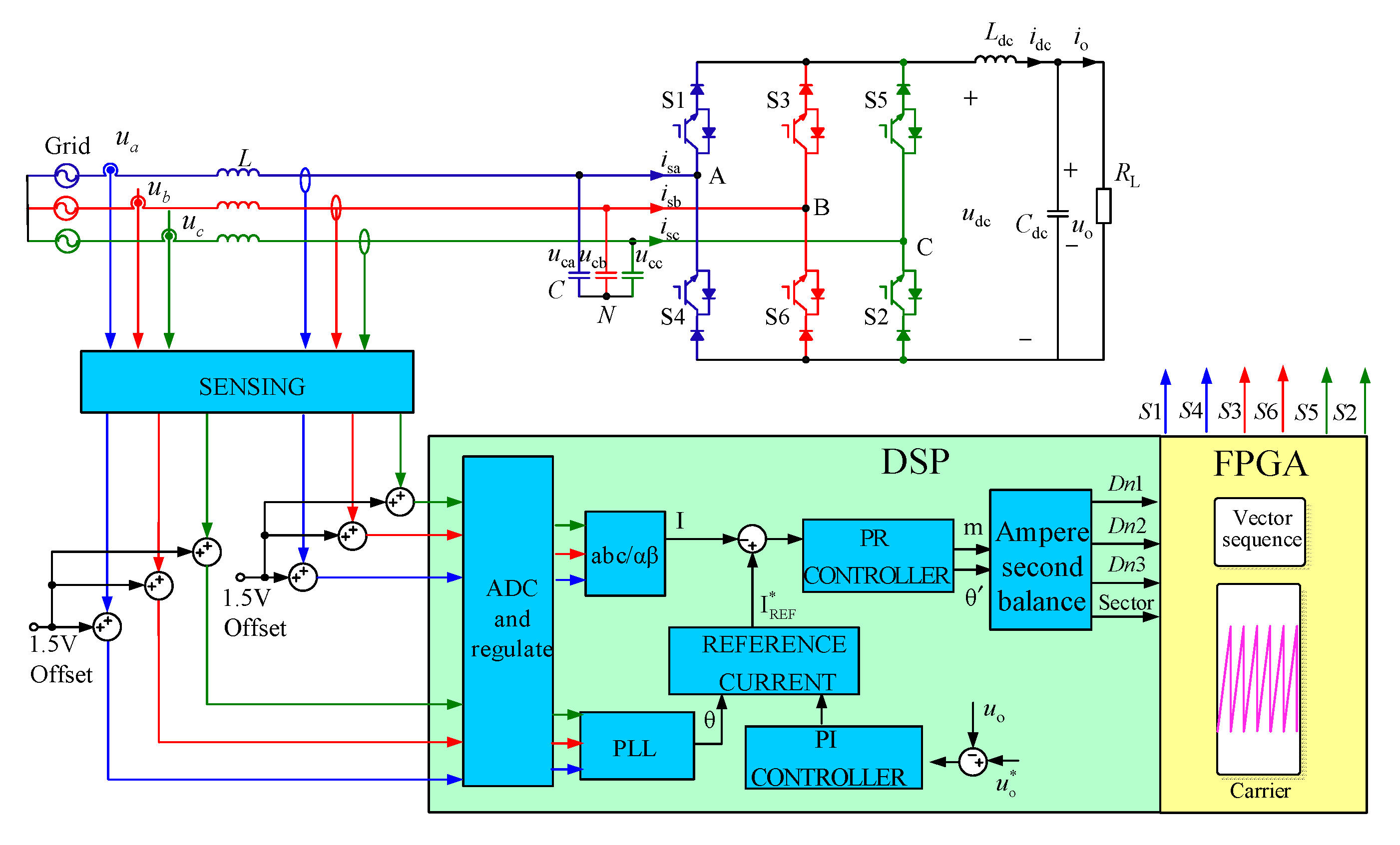
3. Materials and Methods
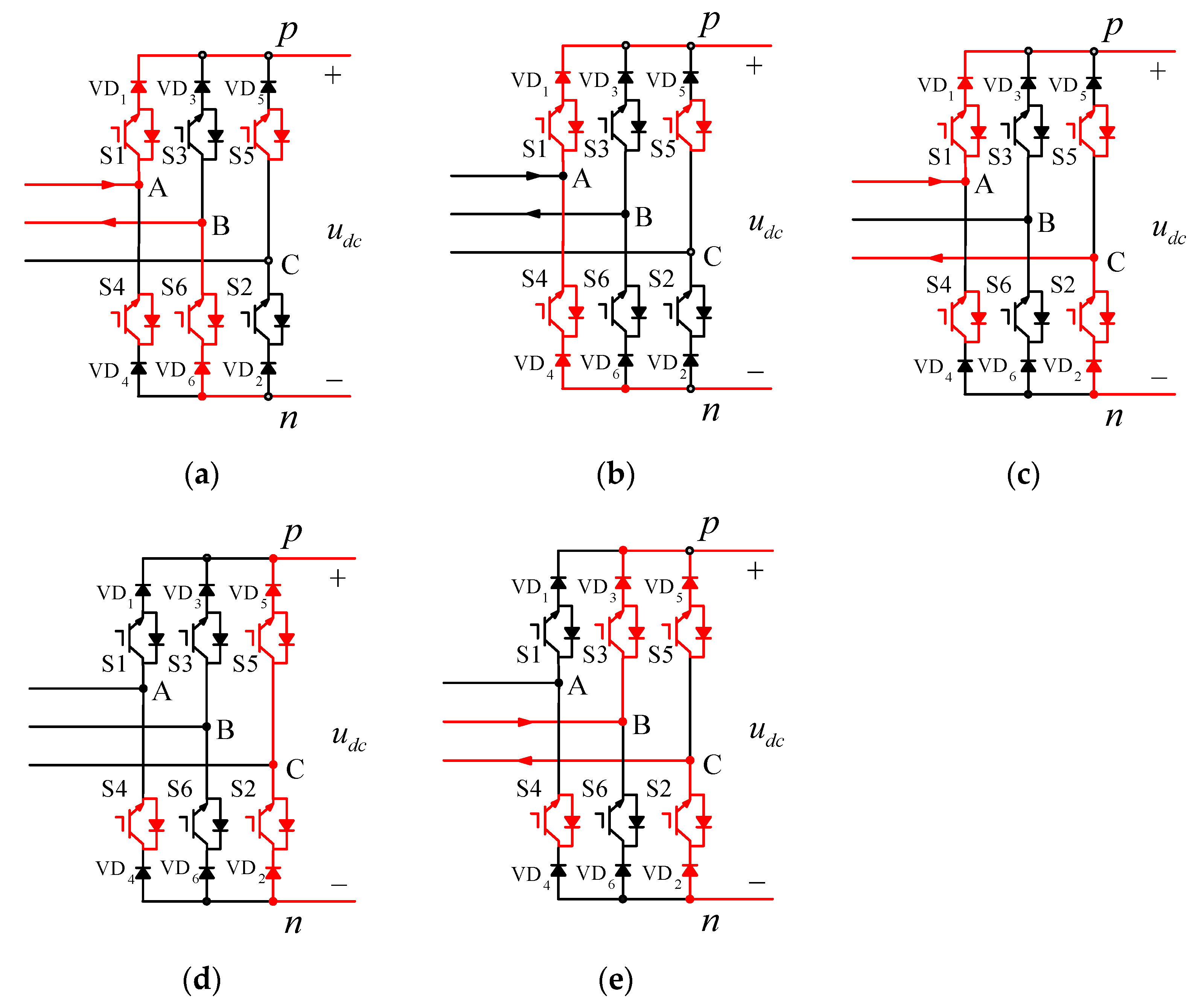
- (1)
- As shown in Figure 7a, the switches S1, S6, S4, S5 receive the turn-on signal and are turned on, but the current can only flow from high voltage to low voltage. In other words, the diodes VD4 and VD5 are subject to reverse voltage because ua > ub > uc, there the inductor current only flows through S1 and S6 at this time.
- (2)
- As shown in Figure 7b, when S6 switches to S2, if the switch S6 to be turned off has been turned off and the switch S2 to be turned on has not been turned on due to the switching characteristics, the current will flow through the freewheeling switch S4, which will avoid discontinuity in the inductor current, and the inductor current flows through S1 and S4 at this time.
- (3)
- As shown in Figure 7c, when the switch S2 is turned on, VD4 is subjected to a reverse voltage at this time, so the inductor current cannot flow through S4, and the inductor current flows through S1 and S2 at this time.
- (4)
- As shown in Figure 7d, when the S1 switches to S3, if the S1 to be turned off has been turned off and the S3 to be turned on has not yet been turned on due to the switching characteristics, the current will flow through the freewheeling switch S5, thus avoiding discontinuity in the inductor current, and the inductor current flows through S2 and S5 at this time.
- (5)
- As shown in Figure 7e, when the switch S3 is turned on, VD5 is subjected to a reverse voltage at this time, so the inductor current cannot flow through S5, and the inductor current flows through S3 and S2 at this time.
4. Main Results
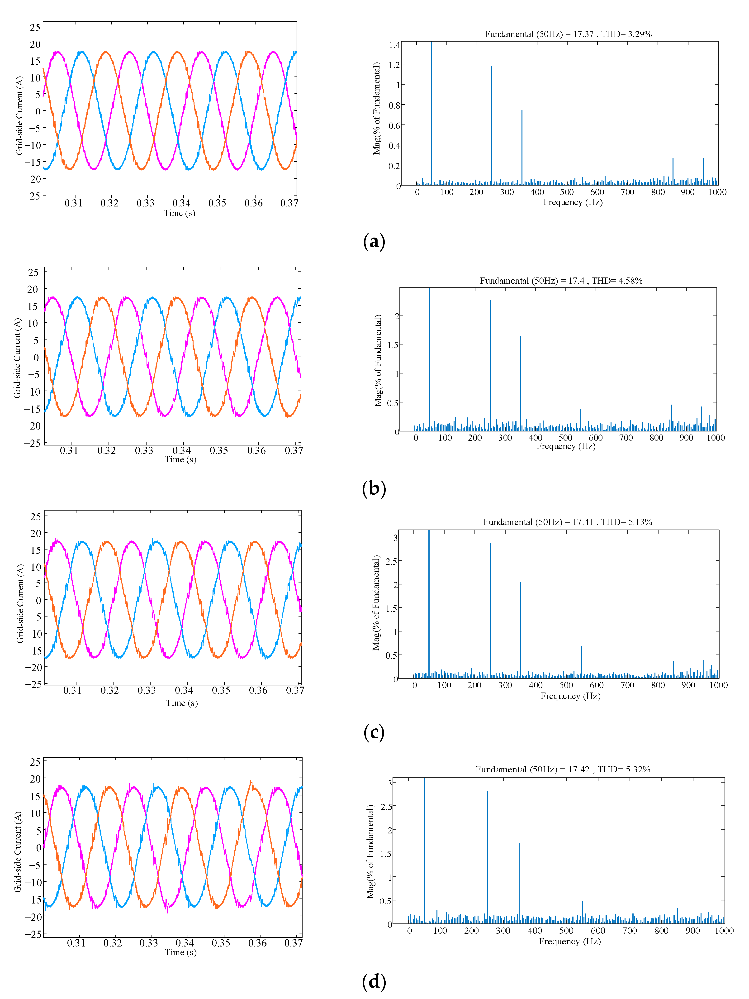
4.1. Results Analysis of Overlap-Time Variation
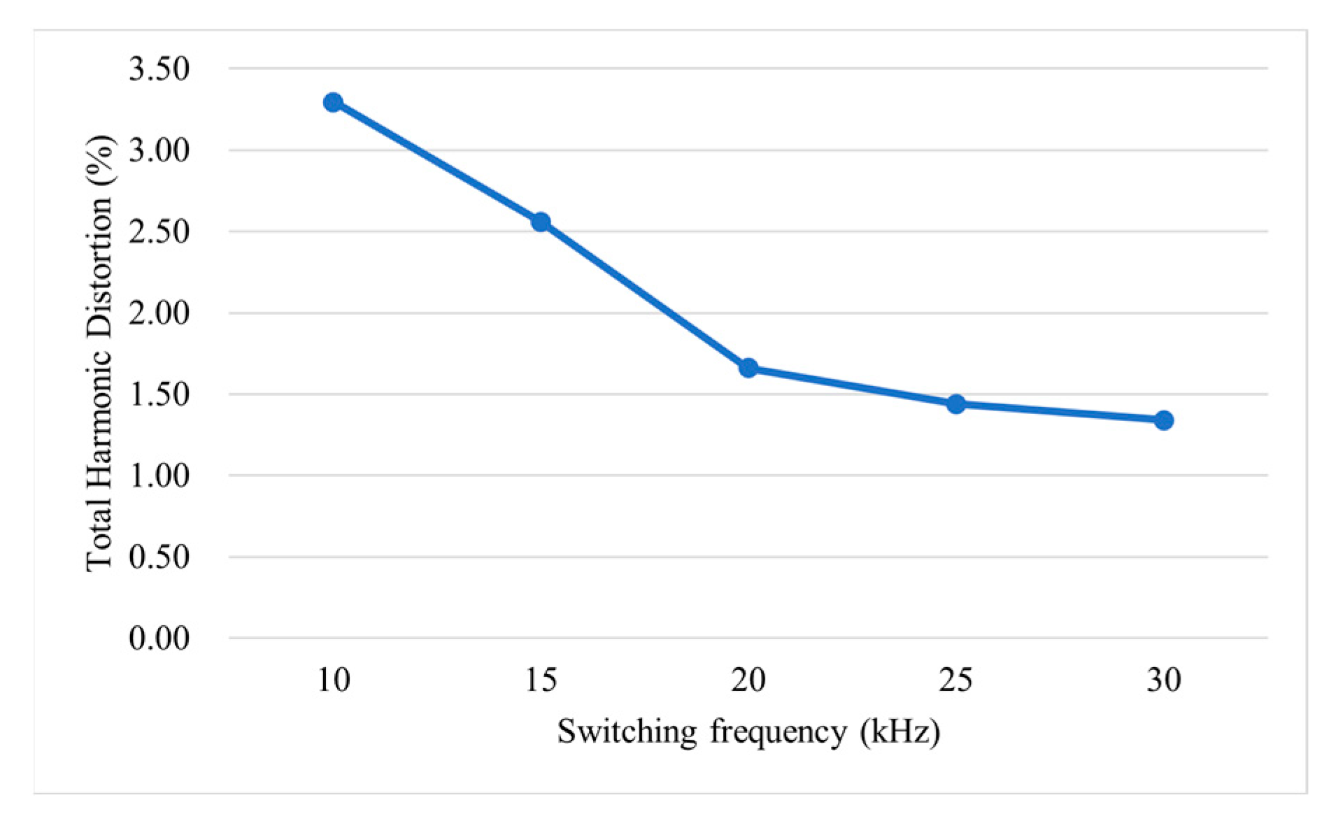
4.2. Results Analysis of Switching Frequency Variation
4.3. Result Analysis of The Proposed Scheme
5. Discussion
6. Conclusions
- (1)
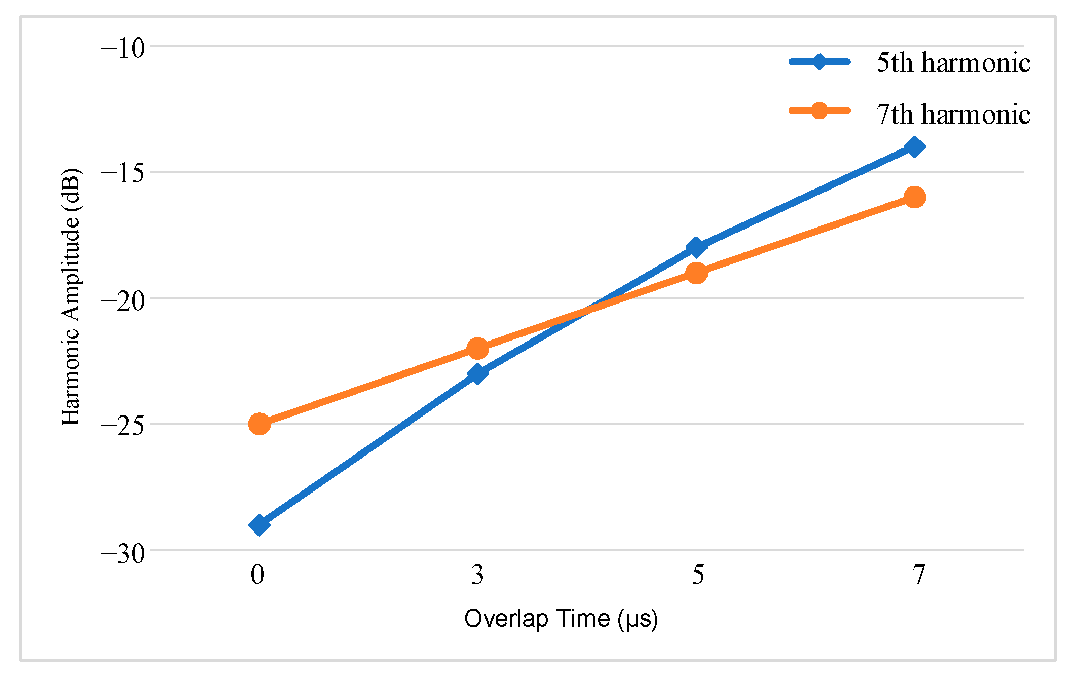
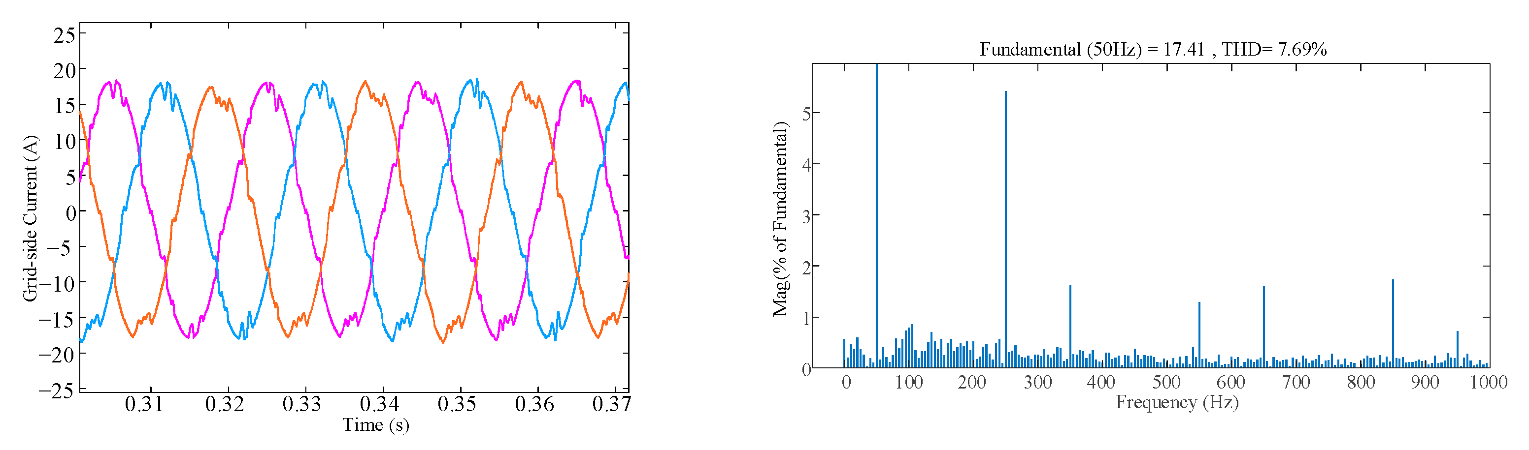
- The overlap time introduces the 6k + 1(k = 1, 2, 3, …) harmonics in the grid current, and these harmonic components increase with the switching frequency and the overlap time.
- (2)
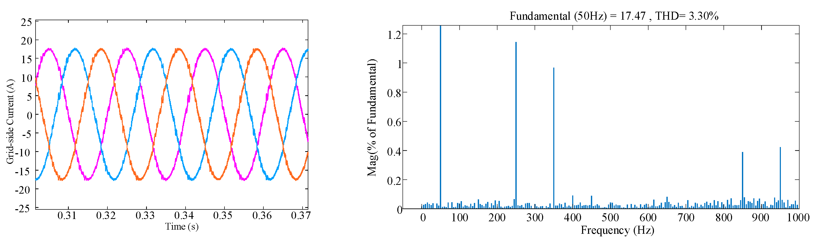
- The proposed method of constructing a freewheeling channel by controlling a specific switch (Freewheeling switch) to maintain conduction can eliminate the low-order harmonics introduced in the grid current by overlap time.
- (3)
- Simulation and experimental results verify the correctness of the theoretical analysis and the validity of the proposed scheme. Moreover, it is worth noting that the overlap-time suppression effect of the proposed scheme is about 100%.
Author Contributions
Funding
Institutional Review Board Statement
Informed Consent Statement
Data Availability Statement
Conflicts of Interest
Abbreviations
| CSC | Current-source converter |
| VSC | Voltage-source converter |
| DC | Direct current |
| AC | Alternating current |
| THD | Total harmonic distortion |
| IGBT | Insulated gate bipolar transistors |
| RC-IGBT | Reverse conducting insulated gate bipolar transistors |
| MOSFET | Metal oxide semiconductor field effect transistor |
| tov | Overlap time |
| FFT | Fast Fourier transform |
References
- Li, P.; Xiong, L.; Wu, F.; Ma, M.; Wang, J. Sliding mode controller based on feedback linearization for damping of sub-synchronous control interaction in DFIG-based wind power plants. Int. J. Electr. Power Energy Syst. 2019, 107, 239–250. [Google Scholar] [CrossRef]
- Li, P.; Wang, J.; Xiong, L.; Wang, Z. Energy-Shaping Controller for DFIG-Based Wind Farm to Mitigate Subsynchronous Control Interaction. IEEE Trans. Power Syst. 2020, 36, 2975–2991. [Google Scholar] [CrossRef]
- Aouichak, I.; Jacques, S.; Bissey, S.; Reymond, C.; Besson, T.; Le Bunetel, J.-C. A Bidirectional Grid-Connected DC–AC Converter for Autonomous and Intelligent Electricity Storage in the Residential Sector. Energies 2022, 15, 1194. [Google Scholar] [CrossRef]
- Wang, H.; Wang, S.; Ding, H.; Shi, C.; Jia, D.; Chen, C.; Guerrero, J.M. An Novel Six-Segment Modulation Strategy for Three-Phase Isolated PFC Converter. Energies 2022, 15, 2598. [Google Scholar] [CrossRef]
- Fu, X.; Wang, H.; Guo, X.; Shi, C.; Jia, D.; Chen, C.; Guerrero, J.M. A Novel Circulating Current Suppression for Paralleled Current Source Converter Based on Virtual Impedance Concept. Energies 2022, 15, 1952. [Google Scholar] [CrossRef]
- Sun, Y.; Liu, Y.; Su, M.; Han, H.; Li, X.; Li, X. Topology and control of a split-capacitor four-wire current source inverter with leakage current suppression capability. IEEE Trans. Power Electron. 2018, 12, 10803–10814. [Google Scholar] [CrossRef]
- Wei, Q.; Wu, B.; Xu, D.; Zargari, N.R. Further study on a PWM current-source-converter-based wind energy conversion system considering the DC-link voltage. IEEE Trans. Power Electron. 2019, 6, 5378–5387. [Google Scholar] [CrossRef]
- Wei, Q.; Wu, B.; Xu, D.; Zargari, N.R. An Optimized Strategy for PWM Current Source Converter Based Wind Conversion Systems with Reduced Cost and Improved Efficiency. IEEE Trans. Power Electron. 2018, 2, 1202–1210. [Google Scholar] [CrossRef]
- Dai, H.; Jahns, T.M.; Torres, R.A. Comparative Evaluation of Conducted Common-Mode EMI in Voltage-Source and Current-Source Inverters using Wide-Bandgap Switches. In Proceedings of the 2018 IEEE Transportation Electrification Conference and Expo (ITEC), Long Beach, CA, USA, 13–15 June 2018; pp. 788–794. [Google Scholar]
- Dai, H.; Jahns, T.M. Comparative investigation of PWM current source inverters for future machine drives using high-frequency wide band gap power switches. In Proceedings of the 2018 IEEE Applied Power Electronics Conference and Exposition (APEC), San Antonio, TX, USA, 4–8 March 2018; pp. 2601–2608. [Google Scholar]
- Dai, H.; Jahns, T.M.; Torres, R.A. Development of High-Frequency WBG Power Modules with Reverse-Voltage-Blocking Capability for an Integrated Motor Drive using a Current-Source Inverter. In Proceedings of the 2018 IEEE Energy Conversion Congress and Exposition (ECCE), Portland, OR, USA, 23–27 September 2018; pp. 1808–1815. [Google Scholar]
- Chen, W.; Li, B.; Xu, D.; Cai, L. A Dead-Time Compensation Method for Voltage Source Inverters. In Proceedings of the 2019 22nd International Conference on Electrical Machines and Systems (ICEMS), Harbin, China, 11–14 August 2019; pp. 1–6. [Google Scholar]
- Gaber, M.; Abdel-Rahim, O.; Orabi, M. Novel Overlap Method to Eliminate Vector Deviation Error in SVM of Current Source Inverters. IEEE Trans. Power Electron. 2021, 2, 2320–2333. [Google Scholar] [CrossRef]
- Jiang, S.; Arraño-Vargas, F.; Shen, Z.; Konstantinou, G. The Impact of Overlap Period on the Stability of Current-Controlled Alternate Arm Converter Based on dq Frame Impedance Analysis. Electronics 2022, 11, 301. [Google Scholar] [CrossRef]
- Rodríguez-Benítez, O.M.; Ponce-Silva, M.; Aquí-Tapia, J.A.; Claudio-Sánchez, A.; Vela-Váldes, L.G.; Lozoya-Ponce, R.E.; Cortés-García, C. Comparative Performance and Assessment Study of a Current-Fed DC-DC Resonant Converter Combining Si, SiC, and GaN-Based Power Semiconductor Devices. Electronics 2020, 9, 1982. [Google Scholar] [CrossRef]
- Bai, Z.; Zhang, Z.; Ruan, X. A natural soft-commutation PWM scheme for current source converter and its logic implementation. IEEE Trans. Ind. Electron. 2011, 7, 2772–2779. [Google Scholar] [CrossRef]
- Sayed, M.G.; Abdel-Rahim, O.; Orabi, M. Comparative Study to Investigate the Effect of Five VS Seven Segment Modulation Sequence on the Waveform Distortion Resulted by the Overlap Time in Current Source Inverter. In Proceedings of the 2019 International Conference on Innovative Trends in Computer Engineering (ITCE), Aswan, Egypt, 2–4 February 2019; pp. 576–580. [Google Scholar]
- Qin, H.; Zhang, X.; Zhu, Z.; Ma, C.; Xu, H. Influence of overlap time on the AC grid current of current source PWM rectifier and restraining method. Trans. China Electrotech. Society. 2016, 12, 142–152. [Google Scholar]
- Liu, P.; Wang, Z.; Xu, Y.; Xiao, H.; Li, Y.W. Optimal Overlap-Time Distribution of Space Vector Modulation for Current-Source Rectifier. IEEE Trans. Ind. Electron. 2021, 6, 4586–4597. [Google Scholar] [CrossRef]
- Geng, Y.; Deng, R.; Dong, W.; Wang, K.; Liu, H.; Wu, X. An Overlap-Time Compensation Method for Current-Source Space-Vector PWM Inverters. IEEE Trans. Power Electron. 2018, 4, 3192–3203. [Google Scholar] [CrossRef]
- Guo, X.; Yang, Y.; Wang, X. Optimal space vector modulation of current-source converter for DC-link current ripple reduction. IEEE Trans. Ind. Electron. 2019, 3, 1671–1680. [Google Scholar] [CrossRef]
- Jacques, S.; Reymond, C.; Le Bunetel, J.-C.; Benabdelaziz, G. Comparison of the power balance in a Totem-Pole Bridgeless PFC Topology with several inrush current strategies. J. Electr. Eng. 2021, 72, 12–19. [Google Scholar] [CrossRef]


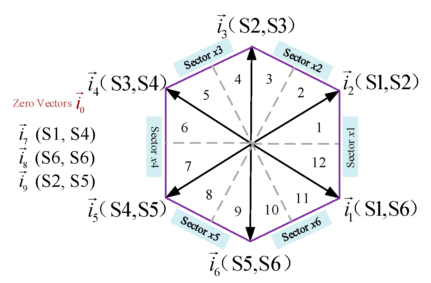
| Type | Space Vector | Switching States |
|---|---|---|
| Active Vectors | i1 | S1, S6 |
| i2 | S1, S2 | |
| i3 | S2, S3 | |
| i4 | S3, S4 | |
| i5 | S4, S5 | |
| i6 | S5, S6 | |
| Zero Vectors | i7 | S1, S4 |
| i8 | S3, S6 | |
| i9 | S2, S5 |
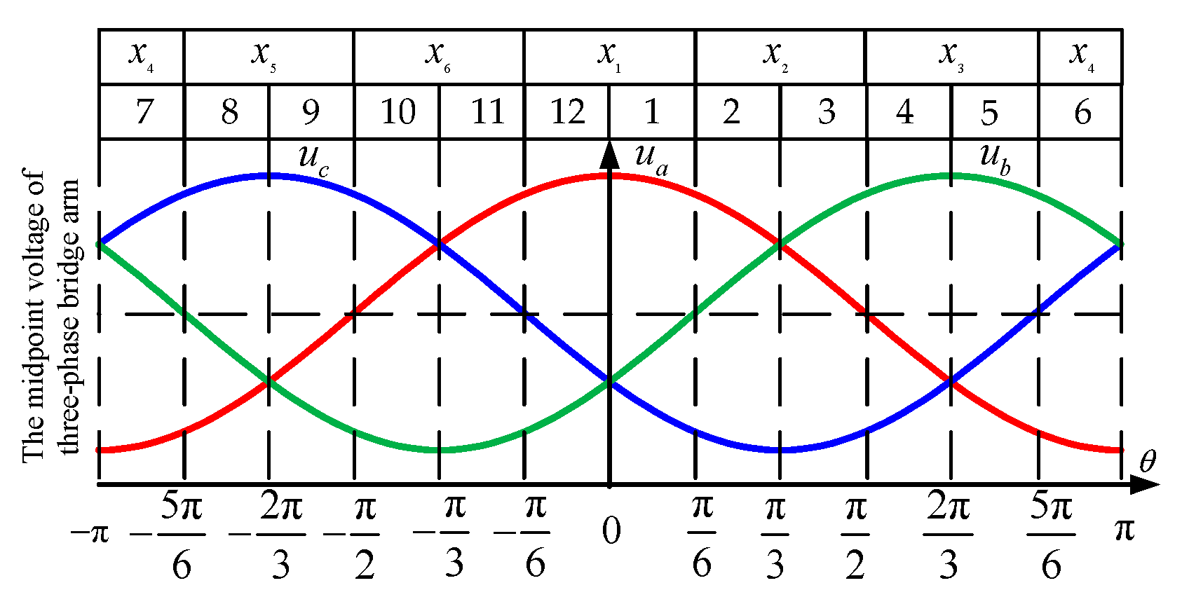
| Sector | Terminal Voltage | |||
|---|---|---|---|---|
| 1 | ua > ub > uc | 0 | ||
| 2 | ua > ub > uc | 0 | ||
| 3 | ub > ua > uc | 0 | ||
| 4 | ub > ua > uc | 0 | ||
| 5 | ub > uc > ua | 0 | ||
| 6 | ub > uc > ua | 0 | ||
| 7 | uc > ub > ua | 0 | ||
| 8 | uc > ub > ua | 0 | ||
| 9 | uc > ua > ub | 0 | ||
| 10 | uc > ua > ub | 0 | ||
| 11 | ua > uc > ub | 0 | ||
| 12 | ua > uc > ub | 0 |
| Sector | Terminal Voltages | Freewheeling Switch |
|---|---|---|
| 1 | ua > ub > uc | S4, S5 |
| 2 | ua > ub > uc | S4, S5 |
| 3 | ub > ua > uc | S5, S6 |
| 4 | ub > ua > uc | S5, S6 |
| 5 | ub > uc > ua | S1, S6 |
| 6 | ub > uc > ua | S1, S6 |
| 7 | uc > ub > ua | S1, S2 |
| 8 | uc > ub > ua | S1, S2 |
| 9 | uc > ua > ub | S2, S3 |
| 10 | uc > ua > ub | S2, S3 |
| 11 | ua > uc > ub | S3, S4 |
| 12 | ua > uc > ub | S3, S4 |
| Parameter | Symbol | Simulation | Experiment |
|---|---|---|---|
| Phase Voltage | Vi | 220 V | 40 V |
| DC Inductance | Lp | 5 mH | 5 mH |
| DC Capacitor | Cdc | 940 μF | 940 μF |
| Filter Inductance | L | 2.5 mH | 4 mH |
| Filter Capacitor | C | 20 μF | 9.4 μF |
| Load | R | 20 Ω | 30 Ω |
Publisher’s Note: MDPI stays neutral with regard to jurisdictional claims in published maps and institutional affiliations. |
© 2022 by the authors. Licensee MDPI, Basel, Switzerland. This article is an open access article distributed under the terms and conditions of the Creative Commons Attribution (CC BY) license (https://creativecommons.org/licenses/by/4.0/).
Share and Cite
Ding, H.; Li, Q.; Yuan, J.; Wang, W.; Li, M.; Guerrero, J.M. A Novel Overlap-Time Effect Suppression for Current Source Converter. Energies 2022, 15, 6035. https://doi.org/10.3390/en15166035
Ding H, Li Q, Yuan J, Wang W, Li M, Guerrero JM. A Novel Overlap-Time Effect Suppression for Current Source Converter. Energies. 2022; 15(16):6035. https://doi.org/10.3390/en15166035
Chicago/Turabian StyleDing, Hao, Quanjie Li, Jing Yuan, Wei Wang, Mingming Li, and Josep M. Guerrero. 2022. "A Novel Overlap-Time Effect Suppression for Current Source Converter" Energies 15, no. 16: 6035. https://doi.org/10.3390/en15166035
APA StyleDing, H., Li, Q., Yuan, J., Wang, W., Li, M., & Guerrero, J. M. (2022). A Novel Overlap-Time Effect Suppression for Current Source Converter. Energies, 15(16), 6035. https://doi.org/10.3390/en15166035