Abstract
A novel modular Transformerless, Self-balanced, Static Synchronous Series Compensator (TSB-SSSC) capable of delivering ultra-high current, with the objective of dynamically balancing the impedance of the transmission power grid, is proposed. Balancing transmission lines is crucial in power optimization and delivery because it increases the power transfer capability without building new power lines. The transformerless SSSC needs to support and control the line current from a few hundred to several thousand amperes. This paper presents how the ultra-high current architecture of the TSB-SSSC is achieved by operating multiple converters with self-balancing capabilities in parallel. The mechanism of self-balancing is based on the intrinsic physics of the capacitor and is enabled by a passive network of capacitor equalizers that keep the capacitor voltage equal during switching disconnection. The second self-balancing system consists of an inductive component that balances possible differences among delay switching caused by the aging of the multiple IGBTs from the different converters that form the SSSC. This work presents the analytical set of equations that describes the system and a complete set of simulations where the effectiveness of self-balancing paralleling topology is shown.
1. Introduction
The traditional power system was centralized, well-planned, and with firm control at the generation center and reasonable control on the centers of consumption. Under these conditions, utility companies could plan the expansion and tie tune of the power system infrastructure. In other words, power lines on the power system could be passively tuned to be able to carry power at close to their potential limits, thereby maximizing installed assets, especially related to transmission power lines.
The arrival of solar and wind power produced a fundamental transformation in the power system’s morphology and control, shifting it from a centralized generation of power to a distributed generation, reducing the controllability of the power system, and adding significant degrees of randomness. Nowadays, there are no specific generation centers anymore, but instead a steadily growing, diversified generation of all the parts of the power system, including what used to be the traditional loads. The modern, distributed power system has dynamics that shift within minutes, depending on solar radiation and wind intensity.
Unbalanced power lines limit the total power transfer from one point to another. The use of passive compensation such as capacitors and inductors to balance the lines is less effective because of the fast changes—within minutes—in power generation. Consequently, the current distribution in power transmission lines has drifted from a design condition to a sub-utilized system, with some power transmission lines carrying more current than others. When a power line reaches its maximum current limit, the overall power transmission is limited as well. Then, power transmission reaches its ceiling regardless of whether other power lines are carrying lower than nominal current.
To solve this problem, there are two effective solutions. The traditional solution consists of constructing more power transmission lines in the congested areas of the power system. Construction of power lines is a complicated and expensive proposition that requires obtaining pass-through permits, buying private land, and usually facing significant political opposition from people objecting to power lines near their homes (see Figure 1). The second solution discussed in this work is using a flexible alternating current transmission system (FACTS) to balance the power lines. FACTS, in general, are power electronics converters to control and enhance the power system’s capabilities. Traditional FACTS are based on shunt structures such as Static synchronous compensator (STATCOM) and static var compensator (SVC). The best representative of a series structure is the SSSC. This work is concentrated in an SSSC that dynamically changes the impedance of the power line to balance the current and allow the system to reach levels near the respective nominal power. Any compensators can be applied to balance power lines. The successful device needs to provide the best cost-benefit possible. Devices in series intrinsically deal with significantly lower voltages, therefore they have a better chance to be successful if a low-cost high-current architecture is achieved as proposed in this work. Consequently, to be practical SSSCs l require an active device with reliable device-manufacturability and self-balance mechanisms at a relatively low cost. A transformerless self-balanced SSSC (TSB-SSSC) is discussed in this work as the solution to this problem because it can shift from an inductive to a capacitive function, balancing the transmission of the power system in either case. As an example, the top diagram of Figure 2 shows how unbalanced power lines limit the transfer of power. Once one line reaches 100% of its nominal power (in this case, the line is indicated as a red arrow), the parallel lines (blue arrow) cannot increase their power; in this example, the parallel line cannot go above 40% of its line nominal power. The maximum power the system can transfer is limited to 70% for the top diagram (power of each line/number of lines); however, the bottom diagram of Figure 2 shows an example in which a TSB-SSSC balances the current, allowing the system to regain the possibility of increasing the power to 100% on each parallel line, thus regaining 30% of the nominal power compared to the unbalanced case.
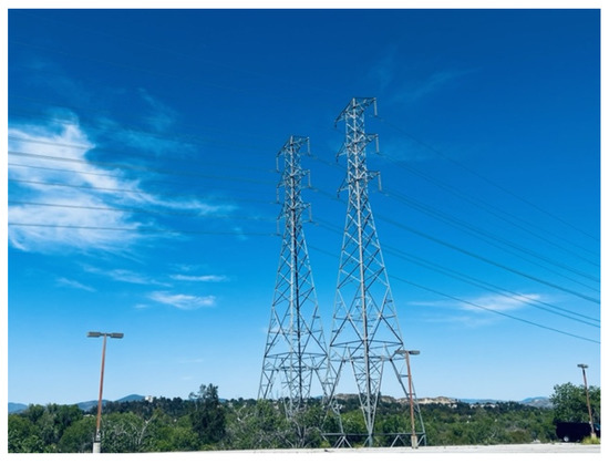
Figure 1.
Parallel transmission power lines in a suburban area in Santa Clarita, CA, USA.
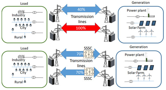
Figure 2.
The unbalance in the transmission power lines can be compensated with TSB-SSSC.
2. Background: Static Synchronous Series Compensator (SSSC)
The SSSC is an inverter connected in series with an AC transmission line. The SSSC does not have a source of real power connected to its DC capacitor. The inverter can be connected directly to a transmission line, or it can be connected through a transformer. The traditional configuration uses a transformer that reduces the current that the semiconductors receive by the turn ratio of the transformer [1].
The SSSC can control the flow of real power on the transmission line when it is connected in series with that line. Figure 3 shows how the power flows along any AC transmission line between bus 1 and bus 2, and it is given by,
where and are the voltage phasors for bus 1 and bus 2, respectively, . is the inductive reactance of the transmission line, and is the real power flowing along the transmission line. Transmission line voltages are generally regulated very tightly, so it is fair to assume that Power flow on AC transmission lines is mostly uncontrollable: the only level of control that transmission line operators have on the network is through modifying its topology, i.e., they can have a line connected to or disconnected from the AC network. The SSSC can dynamically modify the power flow along the AC transmission line as,
where is the AC voltage injected by the SSSC in series with the transmission line. The above equation shows that the SSSC can modify the power flow along a transmission line by either increasing or decreasing it, depending on the phase angle between and the transmission line current . The amount of real power that can be changed on the transmission line also has a linear relationship with . This gives SSSC a great advantage over other types of series compensators, most of which typically have an inverse relationship between the power flow and the control variable.
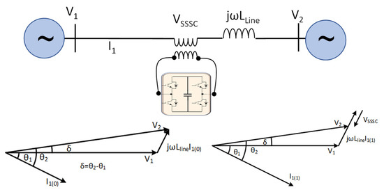
Figure 3.
Basic operation of SSSC with phasor diagram.
This linear control of the power flow along a transmission line makes the SSSC a great tool for transmission line operators and provides them with a lot of flexibility with the changing generation and load profiles in modern power networks. SSSCs are a good option for utilities that generally do not have the flexibility to install additional transmission lines to meet the changes in generation centers resulting from renewables such as offshore wind and distributed solar.
3. Modular SSSC Converter
To balance power system transmission lines, an effective SSSC needs to be capable of injecting from a few to several hundred MWs of reactive power. To inject this amount of reactive power in power lines of several thousand amperes, the SSSC needs to withstand tens of kilovolts. Under these circumstances, the best way to produce a high-power converter is with a modular design such as the one used by Modular Multilevel Converter (MMC) [2,3,4], but with the difference that the SSSC is a series converter that needs to carry the total current of the line at a fraction of the hundreds of kilovolts of the transmission power lines. On the other hand, the MMC is typically used for transmission power systems that sustain the total voltage, usually tens of kilovolts, but only at a fraction of the line current, such as in HVDC or STATCOM applications.
Designing a viable SSSC product must rely on using large-scale manufactured power semiconductors currently on the market. Lower cost and reliable power semiconductors nowadays are centered on silicon IGBTs with a nominal voltage of 1200–1700 V and a current of about a thousand amperes. The operational frequency should be limited to a single pulse or a PWM of a few hundred hertz to avoid significant switching losses. The proposed architecture uses the paralleling converters to carry large line currents in the order of thousands of amperes, and series converters to inject larger voltages in tens of kilovolts [5]. Figure 4 presents a modular arrangement capable of meeting the requirements necessary to develop the transformerless SSSC present in this work.
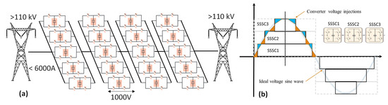
Figure 4.
Modular SSSC scheme (a) diagram (b) 3-seres SCCC single pulse.
The limitation of having a single pulse or a low-frequency wide pulse modulation is that these produce a larger harmonics content compared to a high-frequency PWM. Low harmonics content is addressed with the arrangement of a series converter. Figure 4b shows the scheme for three single pulse converters in series [6]. The concept can be extended to many converters in series that, in combination, produce relatively a very low harmonics content. The analysis of this system for MCC shows the effectiveness of this technique, even with only a small number of converters in series [7].
Strategies to Achieve Large Current in Power Converters
Power converters with large current requirements rely primarily on paralleling modules with self-balancing capabilities before taking advantages of paralleling power converters. Standard power converters require active current balancing [8]. Self-balancing at dies or module levels requires a positive thermal coefficient that intrinsically increases the effective resistance while its temperature increases. As a result of the phenomena, the hotter element pushes the current to the less hot dies, generating an equilibrium when the junction temperature of the different parallel elements is similar. The power semiconductor is based on two fundamental structural components, MOSFETs and IGBTs. The Field Electric Transistor (FET) family is naturally easy to parallel because its conduction is based on the resistive channel with a positive thermal resistance. Based on bipolar technology, IGBT has an intrinsically negative thermal coefficient because higher temperature helps increase the minority carriers’ capacity, effectively increasing the conduction. The modern manufacturers of the power IGBT and diodes add a resistive thermal positive channel to create a net effect of positive thermal coefficient, allowing paralleling of IGBT dies with diodes [9].
Nowadays, large power modules (Figure 5) are the designer’s first tool for producing a sizeable current converter. A large module can be built with up to five or six dies per device. The next step for low-frequency PWM converters is the arrangement of power modules in parallel. A good self-balanced design allows up to four or five power modules; larger quantities of modules require active gating. The unbalanced currents happen during conduction and switching. Logically, balancing control is more difficult during switching. Some authors [10,11,12,13,14,15] propose active balancing control as a solution, especially for converters with high-frequency PWM where switching power losses become dominant. To achieve higher currents with a good performance after the number of modules in parallel is maxed out, the next step of the solution is to connect in parallel active control bridges or converters. SSSCs have particular advantages that can be exploited to connect a large number of converters in parallel, and this is the central contribution of this work.
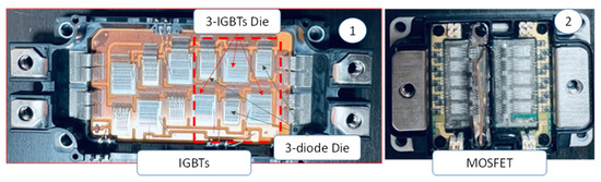
Figure 5.
Modules as single dies paralleling. Panel 1 on the left are the IGBTs and Module. Panel 2 on the right are the MOSFETs.
4. Single Pulse Analysis of SSSC
Another way that the SSSC can be understood is as a variable impedance that behaves as capacitive or inductive, depending on whether the voltage applied to the line is leading or lagging the current. To simplify the explanation, we will use a single pulse injection that presents harmonics related to the pulse’s width, defined by the firing angle α. A simple way to reduce harmonics is to find α that provides the same area below and above the sinusoidal wave. This concept is illustrated in Figure 6.
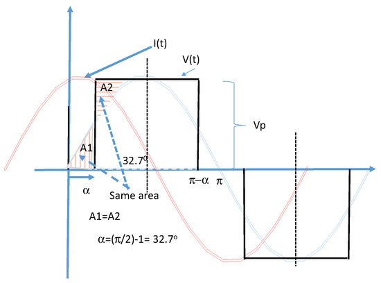
Figure 6.
Square voltage injection and equalized area for harmonics content minimization.
For a given firing angle (α), the first harmonics of the fundamental voltage injection can be calculated as:
By the same area criteria, angle α is calculated to be 32.7°, generating a first harmonic of 1.07 VP, yielding 7% of overmodulation and total harmonic content of less than one-third, which is a relatively small THD (Total Harmonic Distortion), with very low zero-sequence harmonics such as 3rd and 9th harmonics. The maximum injection possible of the first harmonic with α equal to zero produces an overmodulation of 4/π (1.27) with respect to the capacitor voltage, but with one-third of the 3rd harmonic.
The SSSC energy storage is a capacitor limited to a few millifarads; consequently, the voltage of the capacitor does not remain constant. It decreases if the current is leaving or increases if the current fills the capacitor. The depletion of the voltage happens when the inverter is behaving as an inductor; the voltage increase happens when it is behaving as a capacitor. Regardless of behavior, capacitive or inductive, the initial and final capacitor voltage needs to be the same to maintain steady-state operation. Figure 7 shows the “bumping” of the injected AC voltage that can be concave for capacitive injection and convex for inductive injection. The concave or convex shape generates different harmonics content, with the capacitive injection producing less harmonic content. The first harmonics in the two conditions are shown in Figure 7.
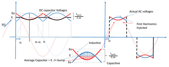
Figure 7.
Concave or convex shape of the voltage depending on inductive or capacitive mode.
A set of Equations (4)–(7) is derived for sizing purposes to compute the first harmonics and the relation with the average capacitor voltages. The equation below shows VAC1 (first harmonic) the relation of line current (IL), firing angle (α), and the initial and final voltage of the capacitor (E). E is defined as open capacitor voltage.
For capacitive mode.
The average voltage on the capacitor is shown in the equation,
For inductive mode,
5. Static Series Synchronous Compensator (SSSC) Principle
The fundamental principle of the proposed topology is based on the capacitor as the only energy source. Capacitors connected in parallel share the same voltage. For this reason, the only factor that determines their current is the value of their capacitances. Therefore, SSSC converters in parallel in the architecture presented in Figure 4a, are naturally self-balanced (see Equation (8) below). For standard converters, the power is fed by a voltage source that does not have intrinsic regulation of the current that takes different paths based on each path’s impedance. For this reason, a voltage source converter needs active compensation to balance the current for each converter in parallel. Details of the self-balancing SSSC are explained in Figure 8.
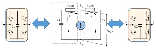
Figure 8.
Self-balancing Principle.
In Figure 8, the power line is represented as a current source (IL), and the two converters (inverters) at any given moment can be represented as a capacitor (C1 and/or C2) connected through a small impedance, representing the power semiconductor switches’ impedance during conduction (RDSON) plus the bus bar and its connections, which is the lumped impedance defined as ZIGBT at each converter. It is clear these equivalent impedances are not linear and have a high dependency on temperature, and may significantly differ from one to another. However, the voltage drops across them are quite small as compared to the capacitor voltage at line frequencies, so the capacitor voltage tends to dominate the current sharing as seen below.
For any capacitor:
Per Kirchhoff’s law:
Since the IGBT impedances during conduction are very small:
and for f < 100 Hz
Then,
The self-balancing methodology consists of simply ensuring the same voltage in the capacitor banks, mainly by utilizing the same capacitance value C1 = C2 for each converter. Consequently, the current IC1 and IC2 will be the same, and, therefore, half of the line current. This principle is extensible to many inverters in parallel (Figure 4a), and as long the capacitors are the same, the current will be distributed equally among the converters. Any slight difference in the capacitor banks will be reflected in current differences, which is the only practical limitation of this application.
6. SSSC Self-Current Balancing Network Equalizer
When the capacitors are in parallel, the value of the capacitances defines the current, as was discussed before. However, the capacitors are connected and disconnected at the PWM frequency by the inverter. After the capacitors are disconnected, they may not have the same voltage anymore. In addition, when reconnected, they may not connect at precisely the same time, allowing a discharge of the first capacitor that is connected, changing its voltage. This condition generates two problems that are analyzed here.
- When the capacitors are disconnected: The voltages of independent capacitor banks can drift differently because of different internal losses and, more critically, if the disconnection did not happen precisely at the same time (a small difference in turn-off time), then the last converter capacitor bank to be disconnected loses or gains additional charge, leading to different voltage among the now-disconnected capacitor banks from each converter.
- When capacitors are reconnected: Even if the disconnected capacitor banks have the same voltage, when they are reconnected, different delays in switching to connection (a small difference in turn-on time) will cause the first converter capacitor bank connected to charge or discharge to a voltage different than the second converter capacitor bank connected.
In both cases, it produces different voltages in the capacitor banks during reconnection, which will create ultra-high circulating currents on the order of tens to hundreds of thousands of amperes between the capacitors. This is because the busbars and the power modules only offer a few nanohenries of inductance to limit the di/dt between the capacitors. This destroys the converter or ages it very quickly. To avoid the described problems, the following two equalizer circuits are designed:
The resistive network equalizer whose role is to ensure very similar voltages when the capacitors are disconnected. The resistance of the network equalizer needs to be large enough compared to the Ron of the semiconductors but low enough to equalize the voltage of the capacitors.
The criterion is,
R equalizer > 100 Ron semiconductor
The differential-mode chokes are inductors (L) that function to limit the current that can occur due to the differences in the turn-on and turn-off among the semiconductors within each converter.
Differences in semiconductors’ turn-on and turn-off times are due to slight differences during the manufacturing process and are accentuated as semiconductors’ aging takes place. Different usages, such as in the example in Figure 4b, where each of the SSSCs in series has different conduction times, imply that the IGBTs will not age at the same rate over time [16,17].
These inductors are small, on the order of several of microhenries, and the criterion for how to dimension them is explained below.
The criterion is:
where:
VL = Module nominal voltage;
ΔI = Line current;
Δt = 50% of the semiconductor turn-off time.
The general goal of the power systems industry is to connect multiple IGBTs in parallel (Figure 9a) to achieve higher continuous current conduction ratings. As discussed in the previous section, paralleling of H-bridges (Figure 4a) in addition to IGBTs, gives extra advantages over only paralleling IGBTs directly, but presents some challenges previously introduced and further reviewed below.
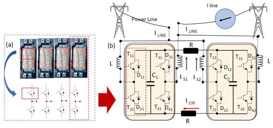
Figure 9.
Embedding paralleling strategy from dices to modules to converters with inductive and resistive balancing network (R and L). (a) Four parallel modules form one IGBT; (b) One converter leg (red dotted line on panel (b)) is formed by four modules as indicated in top portion of panel (a), or bottom circuit diagram of panel (a).
In the ideal case, two inverters are directly connected at their AC terminals, whereas their capacitor terminals are connected in parallel. In real circuits the capacitor voltages could be different, generating a large current; to limit this current, both converters are connected through resistances R (see Figure 9b). The purpose of having R in the circuit is to equalize the DC voltage that develops across the capacitors C1 and C2 before and after voltage injection. Adding resistor R, as in Figure 9b, mitigates the effect resulting when all the IGBTs in parallel inverters perform differently during transient; i.e., they turn on and off at different times. The selection of the value of R is described in Equation (9).
The second problem introduced in the previous section occurs when there are different turn-on and turn-off times across the IGBTs, which can create a shoot-through. To explain this further, let’s consider the example where the positive and negative rails of the DC bus are connected in transients when T11 and T42 (from Figure 9b) are either completely or partially on. This situation can lead to a shoot-through wherein the di/dt is only being controlled by the bus bars’ small inductance. To prevent a rapid current increase, an alternate inductor L is added to the topology, enabling di/dt control.
Figure 9b shows four inductors L between the two inverters. Generally, all inductors have the same value. The selection of L can be carried out based on:
(a) the DC bus voltage level,
(b) the time when the two switches are inappropriately connected (typical worst-case switching transient overlap between the top and bottom switches), and
(c) the transient current handling capability of the IGBTs selected.
The inductors can be split into two to make the design of both inverter units identical to each other. The specification of L is denoted in Equation (10).
The equalizer networks can be extended to more than two converters. In contrast, the two inductors L and the terminals of the converter can be generalized in the same fashion for multiple converters in parallel, but in the case of the resistors R, the network needs a special geometrical arrangement. Figure 10 shows how the network equalizer is extended to three and five converters in parallel.
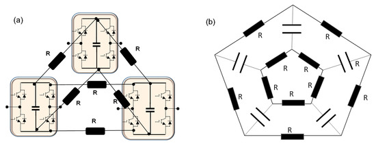
Figure 10.
Resistive equalizer networks for three and five inverter networks. (a) Detailed three converters in paralleling; (b) Simplified view of five converters in paralleling.
7. Results from Analyses and Simulations
The analysis performed for the SSSC is validated by the simulation with PSIM, according to the diagram in Figure 11. The IGBTs assume 1200 V nominal, setting the design limit to the capacitor’s (DC) voltages at 800 V; consequently, the maximum nominal voltage without overmodulation is 560 Vrms. The two converters (S1 and S2) carry half of the line current set at 2000 A rms. The network equalizer parameters are defined as R and L. The parameters are set and defined in Table 1.
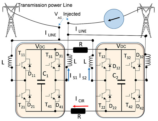
Figure 11.
Two SSSC converters diagram.

Table 1.
Parameter.
7.1. Single-Pulse Validation Analysis
The single pulse of the voltage injected for capacitive and inductive modes with a firing angle of 32.7° is shown in Figure 12a,b, respectively. The maximum operating voltage of the capacitors is set at 800 V as a requirement for protecting the power semiconductors (1200 V). Due to its convex form, the capacitor voltage has an “open” voltage (E) set below the maximum capacitor voltage allowed (800 V), giving space to grow inside a safe area of operation. In contrast, the inductive mode depletes the capacitor that exhibits the convex form and defines the open or not connected voltage (E) as the maximum voltage of the system. This process is expected because “electrical energy” accumulated in the capacitor must be transformed or mimic a “magnetic energy” to behave as an inductor. In Figure 12, the capacitive wave is closer to the sinusoidal shape than the inductive injection for a similar reason to the explanation above.
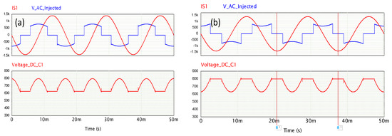
Figure 12.
PSIM output voltage and current for (a) capacitive; (b) inductive injection mode.
The voltage injected for the first harmonic approximation and presented in Equations (4) and (6) is compared using several open voltages (E). The open voltages are varied from 300 to 800 V, and three conditions are calculated for injection capacitive (CAP) and inductive (IND) modes. The first condition consists of computing the first harmonic of the injected RMS voltage by using Equations (4) and (6), which is denoted as IND-F and CAP-F for inductive and capacitive first harmonic voltage, respectively. The second condition consists of determining the same first harmonic but computed by simulation (S1), where the capacitive and inductive first harmonic voltages are denoted CAP-S1 and IND-S1, respectively. The last condition uses PSIM as well, to compute the total RMS of the injected wave that includes all the harmonics generated for the no sinusoidal shape and is defined as CAP-RMS and IND-RMS as total harmonics capacitive or inductive voltage, respectively.
Figure 13 compares the formula results with the simulation. As can be seen, both results are nearly the same, mainly because the simulation does not have an ideal capacitor, bus bar, and IGBTs with an RDSon of 1 ohm, but it includes its parasitic component. These results validate the derivation of the relationship between E and the injected AC voltage. They provide an important tool for setpoint in open-loop control and design in general.
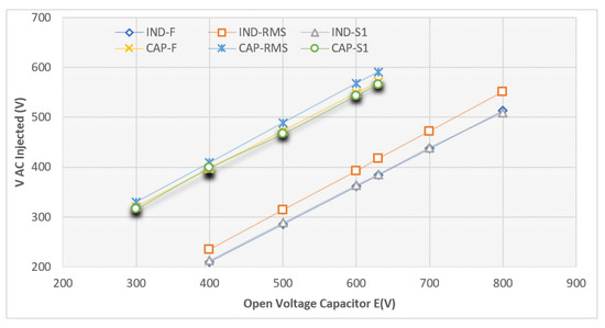
Figure 13.
Comparison of the first harmonics and total Vrms by simulation and theoretical calculation in capacitive and inductive mode.
Another critical aspect of these results is that the RMS value is very similar to the first harmonics, denoting a low harmonic content; it is very low for the capacitor, reaching only 3%, while for inductive mode, it is slightly higher, reaching 10% on average. The capacitor mode can inject about 12% more reactive power than the inductive injection can.
7.2. Self-Balancing and Network Equalizer under Time Delay in Semiconductor
The proposed self-balanced system is tested at a low PWM switching frequency of 360 Hz, and its simulation is shown Figure 14a. Top plots of this figure show the inductive voltage injected and half of line current in order to provide a better scale for voltage comparison. The middle plot shows that the two currents of the converters IS1 and IS2 are identical. For illustration purposes, the Converter 2 current is shifted 180o to avoid superposition with the Converter 1 current. The bottom panel displays the circulating current (ICIR) as zero, confirming full balance operation.
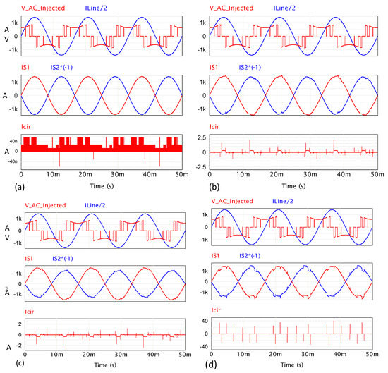
Figure 14.
Outputs of the system with: (a) two identical converters; (b) Converter 2 with 20% higher impedance than converter 1; (c) 20% different capacitors’ banks; (d) 10% different capacitors’ bank and 1 us IGBTs’ time delay.
To verify the effectiveness of the self-balance mechanisms, Converter 2 (S2) is assigned with 20% more impedance across all its components, including RDSON from all IGBTs, the bus bar, and the capacitors’ internal parasitic impedances. Figure 14b shows that even after increasing all Converter 2 parameters by 20%, the dominant effect of the capacitor bank is that it creates a very similar current in both converters, with a difference of less than 2%, showing the effectiveness of the proposed technology, independent of natural differences in converters due to manufacturing and aging. Note that the circuit current (ICIR) is less than 200 mA. Figure 14c shows the unbalances in the capacitor banks when they are 20% different, with C1 = 10 mF and C2 = 8 mF. The capacitors’ proportional difference is transferred to the current, but the parallel converters work in a stable fashion. The current IS1 increases by 10%, and IS2 reduces by the same amount, accounting for a total of 20% variation between the capacitances. The circulating current (ICIR) grows to 1.5 A, demonstrating a stable system. The three previous examples indicate how the circulating current can be used as feature indicator of premature aging of the capacitor banks.
A more demanding test is combining two major unbalanced conditions. The first is a 10% difference in the capacitor banks, setting C1 = 10 mF and C2 = 9 mF, and, more critically, the second is a forced 1 us delay in the turn-on command of IGBTs T11 and T21 in Converter 1. Figure 14d shows that the current of each converter becomes distorted, but in a nearly balanced and complementary fashion. The only unbalance is in proportion to the corresponding differences in the capacitors’ bank and the transient unbalance due to the switching delay that is reduced by the equalizer network. The circulating current, ICIR, shows a fast peak of 40 A. and an RMS value less than 8 A.
The simulation in Figure 15 is a repetition of Case (d) from Figure 14 without R and L, which means R is infinite (open circuit), and L is zero (short circuit) to show the effectiveness of the proposed balancing network. The results shown in Figure 15 demonstrates that the current in each converter grows over 25 kA, and the IGBTs are subject to over voltages close to 2 kV; thus, both conditions will destroy the IGBTs.
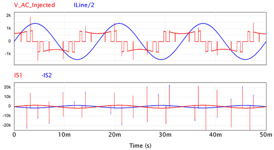
Figure 15.
Repetition of case (d) from Figure 14 without balancing network.
7.3. Network Equalizer Components Tolerance Evaluation
The network equalizer tolerance to variation in its components is evaluated under changes of 50% of its set of resistances (R) and inductances (L) values. Four unbalanced SSSC converters with the corresponding network equalizers were simulated (doubling the system in Figure 11). For two of the SSSC converters as illustrated in Figure 11, the simulated network equalizer consisted of a perfect equalizer with two resistors of 10 ohms and four inductances of 1 uH. For the other two unbalanced SSSC converters the network equalizer was unbalanced by varying its resistances by 50%, which was achieved by leaving the top resistor R1 = 10 ohm and increasing the bottom to R2 = 15 ohms. Similar variation was applied to the inductances of the second pair of SSSC converters, augmenting their value from 1 to 1.5 uH. The top plot in Figure 16 shows the difference in circulating current between the two pair of SSSC converter, which is very small. The RMS value of the difference is less than 1.25 A under currents of 1000 A rms. These results verify the effectiveness and robustness of the equalizing system, and its high tolerance for network resistance and inductance variations.
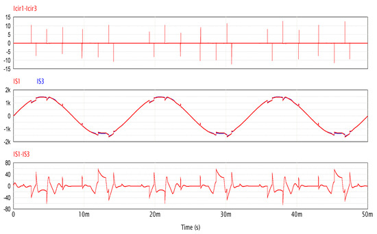
Figure 16.
Evaluation of the network equalizer tolerance to variation.
8. Conclusions
The viability of the scalable architecture to alleviate and improve congested power transmission lines based on a modular transformerless self-balanced SSSC (TSB-SSSC) is proposed and validated by simulation. An inductive and resistive equalizer network compensates for the unsymmetric operation of each converter caused by manufacturing process, aging, and/or semiconductor gating delays. The network equalizer’s fundamental operation principles are described, and criteria for resistive and inductive components’ selection and arrangement are established. The mathematical analysis for one pulse voltage injection for inductive and capacitive mode was demonstrated and verified in simulations.
Funding
This research received no external funding.
Institutional Review Board Statement
Not applicable.
Informed Consent Statement
Not applicable.
Data Availability Statement
Not applicable.
Acknowledgments
The author thanks Govind Chavan for his contribution on the symmetrical arrangement of the inductor equalizer network, and him and Shreesha Adiga Manoor for their time discussing the presented architecture. Thanks to Haroon Inam for his vision, leadership, and support in this project, and lastly, many thanks to technical writer Bridget Heneghan for her excellent editing of this work.
Conflicts of Interest
The author declares no conflict of interest.
References
- Chavan, G.; Bhattacharya, S. A novel control algorithm for a static series synchronous compensator using a Cascaded H-bridge converter. In Proceedings of the 2016 IEEE Industry Applications Society Annual Meeting, Portland, OR, USA, 2–6 October 2016; pp. 1–6. [Google Scholar] [CrossRef]
- Gontijo, G.; Wang, S.; Kerekes, T.; Teodorescu, R. New AC-AC Modular Multilevel Converter Solution for Medium-Voltage Machine-Drive Applications: Modular Multilevel Series Converter. Energies 2020, 13, 3664. [Google Scholar] [CrossRef]
- Sharifabadi, K.; Harnefors, L.; Nee, H.P.; Norrga, S.; Teodorescu, R. Introduction to Modular Multilevel Converters. In Design, Control, and Application of Modular Multilevel Converters for HVDC Transmission Systems; IEEE: Piscataway, NJ, USA, 2016; pp. 7–59. [Google Scholar] [CrossRef]
- Vechalapu, K.; Bhattacharya, S. Modular multilevel converter based medium voltage DC amplifier for ship board power system. In Proceedings of the 2015 IEEE 6th International Symposium on Power Electronics for Distributed Generation Systems (PEDG), Aachen, Germany, 22–25 June 2015; pp. 1–8. [Google Scholar] [CrossRef]
- Moodie, A.; Taheri-Nassaj, N.; Farahani, A.; Ginart, A. Integration of a Power Flow Control Unit. U.S. Patent 11,342,749, 24 May 2022. [Google Scholar]
- Ginart, A.; Stuber, M.T.G.; Inam, H.; Manoor, S.A. Modular Time Synchronized Injection Modules. U.S. Patent 11,121,551, 14 September 2021. [Google Scholar]
- Raman, S.R.; Cheng, K.W.E.; Ye, Y. Multi-Input Switched-Capacitor Multilevel Inverter for High-Frequency AC Power Distribution. IEEE Trans. Power Electron. 2018, 33, 5937–5948. [Google Scholar] [CrossRef]
- Keller, C.; Tadros, Y. Are paralleled IGBT modules or paralleled IGBT inverters the better choice? In Proceedings of the 1993 Fifth European Conference on Power Electronics and Applications, Brighton, UK, 13–16 September 1993; pp. 1–6. [Google Scholar]
- Ginart, A. (Ed.) Fault Diagnosis for Robust Inverter Power Drives; Energy Engineering; IET: London, UK, 2019; Volume 120. [Google Scholar]
- Schlapbach, U. Dynamic paralleling problems in IGBT module construction and application. In Proceedings of the 2010 6th International Conference on Integrated Power Electronics Systems, Nuremberg, Germany, 16–18 March 2010; pp. 1–7. [Google Scholar]
- Tang, Y.; Ma, H. Dynamic electrothermal model of paralleled IGBT modules with unbalanced stray parameters. IEEE Trans. Power Electron. 2016, 32, 1385–1399. [Google Scholar] [CrossRef]
- Xing, K.; Lee, F.C.; Boroyevich, D. Extraction of parasitic within wire-bond IGBT modules. In Proceedings of the APEC’98 Thirteenth Annual Applied Power Electronics Conference and Exposition, Anaheim, CA, USA, 15–19 February 1998; Volume 1, pp. 497–503. [Google Scholar]
- Schnell, R.; Hartmann, S.; Truessel, D.; Fischer, F.; Baschnagel, A.; Rahimo, M. LinPak, a new low inductive phase-leg IGBT module with easy paralleling for high power density converter designs. In Proceedings of the PCIM Europe 2015, International Exhibition and Conference for Power Electronics, Intelligent Motion, Renewable Energy and Energy Management, Nuremberg, Germany, 19–20 May 2015; pp. 1–8. [Google Scholar]
- Bortis, D.; Biela, J.; Kolar, J.W. Active gate control for current balancing of parallel-connected IGBT modules in solid-state modulators. IEEE Trans. Plasma Sci. 2008, 36, 2632–2637. [Google Scholar] [CrossRef]
- Regnat, G.; Jeannin, P.-O.; Frey, D.; Ewanchuk, J.; Mollov, S.V.; Ferrieux, J. Optimized power modules for silicon carbide MOSFET. IEEE Trans. Ind. Appl. 2017, 54, 1634–1644. [Google Scholar] [CrossRef]
- Brown, D.W.; Abbas, M.; Ginart, A.; Ali, I.N.; Kalgren, P.W.; Vachtsevanos, G.J. Turn-off time as an early indicator of insulated gate bipolar transistor latch-up. IEEE Trans. Power Electron. 2011, 27, 479–489. [Google Scholar] [CrossRef]
- Malik, A.; Haque, A.; Kurukuru, V.S.B.; Khan, M.A.; Blaabjerg, F. Overview of Fault Detection Approaches for Grid Connected Photovoltaic Inverters. e-Prime-Adv. Electr. Eng. Electron. Energy 2022, 2, 100035. [Google Scholar]
Publisher’s Note: MDPI stays neutral with regard to jurisdictional claims in published maps and institutional affiliations. |
© 2022 by the author. Licensee MDPI, Basel, Switzerland. This article is an open access article distributed under the terms and conditions of the Creative Commons Attribution (CC BY) license (https://creativecommons.org/licenses/by/4.0/).