
Development of a Bidirectional DC–DC Converter with Rapid Energy Bidirectional Transition Technology


Abstract
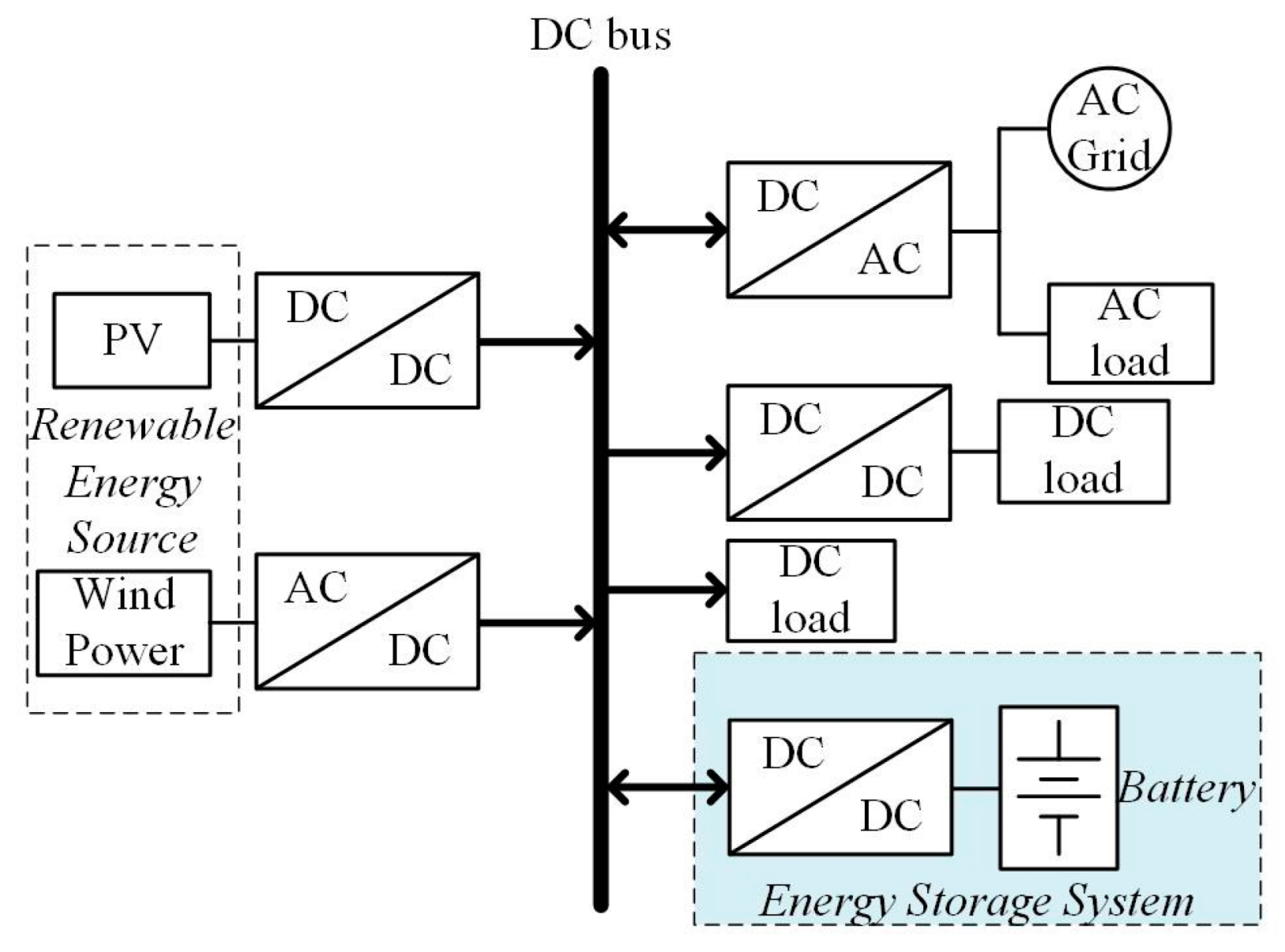
:1. Introduction
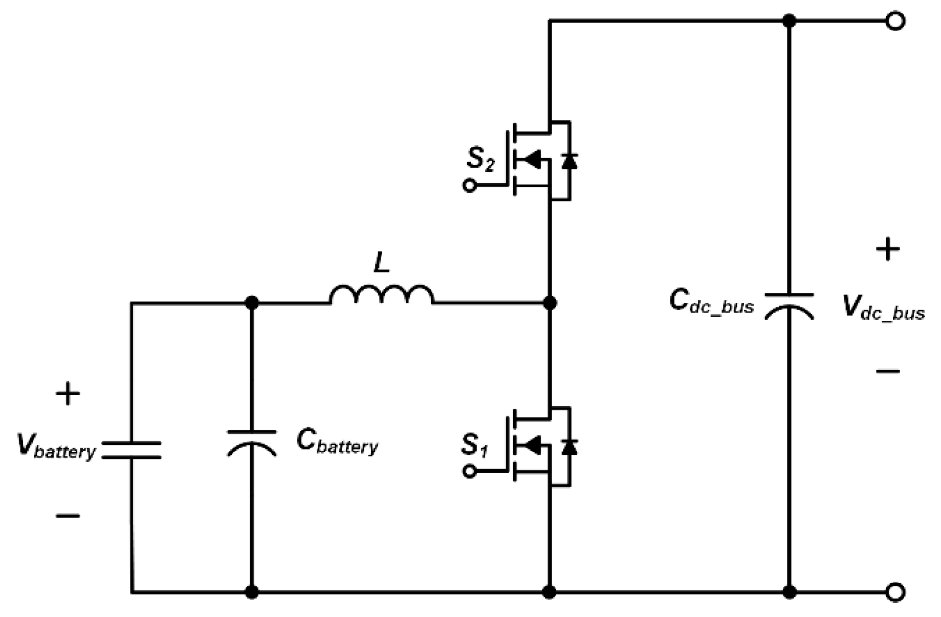
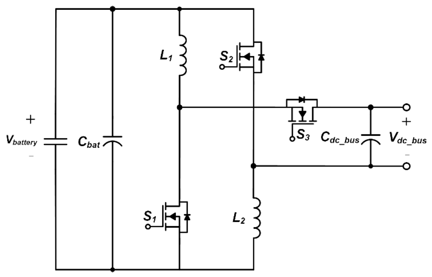
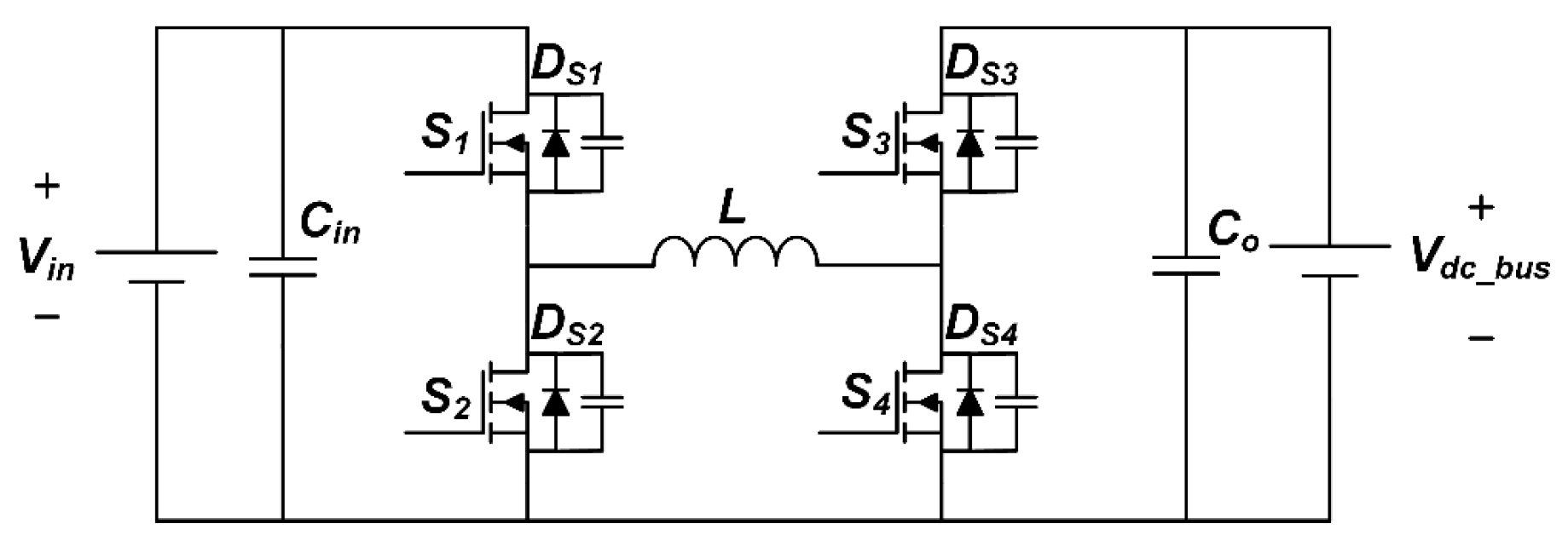
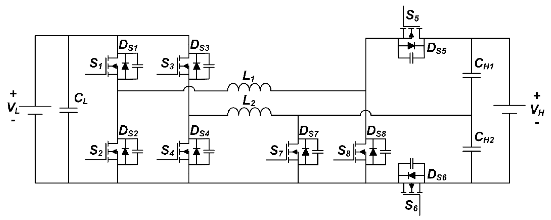
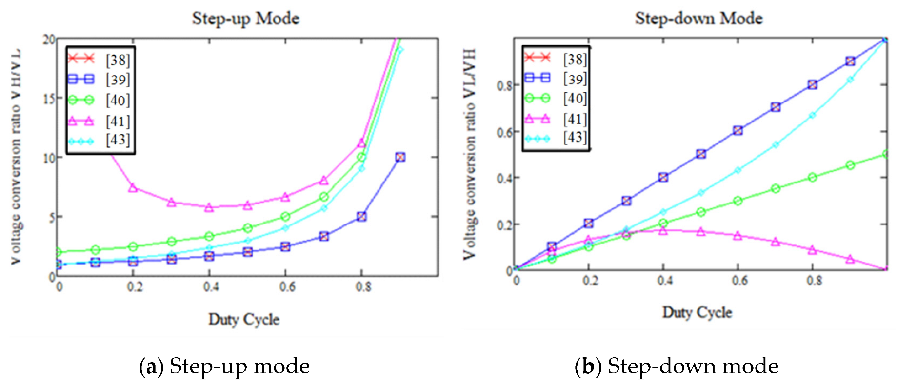
2. Reviews of Bidirectional DC–DC Topologies
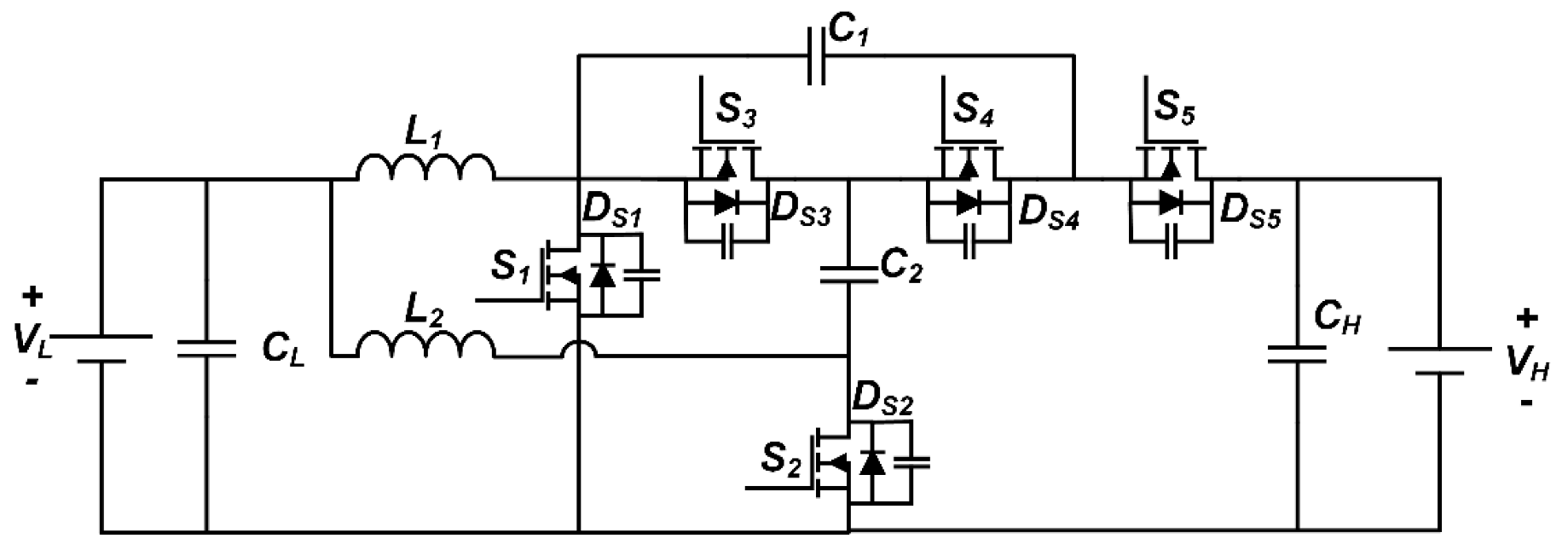
3. Technique and Control Strategy of Rapid Energy Conversion
3.1. Transition Operation Mode Analysis
- (a)
- The capacitance of Clow and Chigh were large enough to make the voltage across the capacitor constant.
- (b)
- The body diodes of all power switches were considered.
- (c)
- All components were ideal, and the impact of the dead time of the driving signal was ignored.
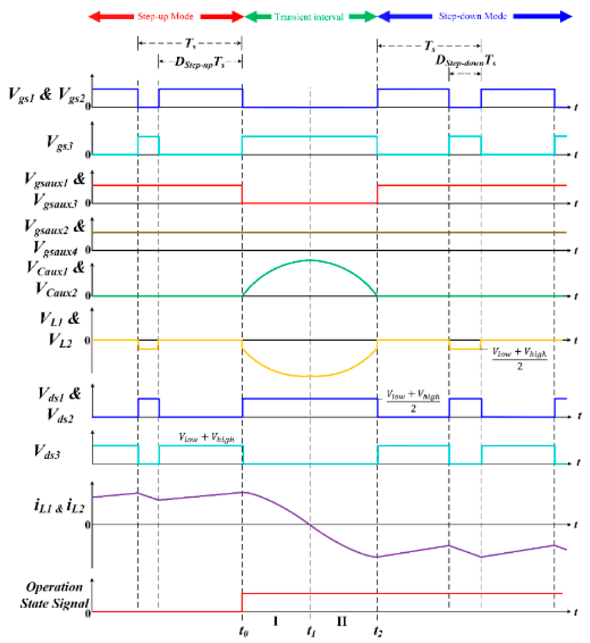
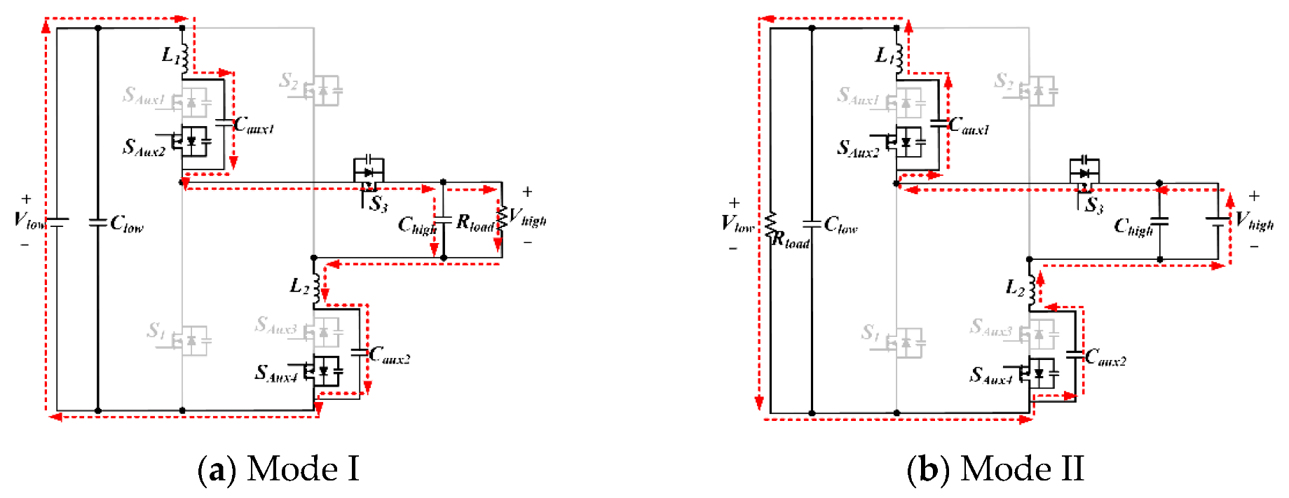
3.1.1. Transition from Step-Up Mode to Step-Down Mode
Step-Up Mode to Step-Down Mode I (t0–t1)
Step-Up Mode to Step-Down Mode II (t1–t2)
3.1.2. Transition from Step-Down Mode to Step-Up Mode
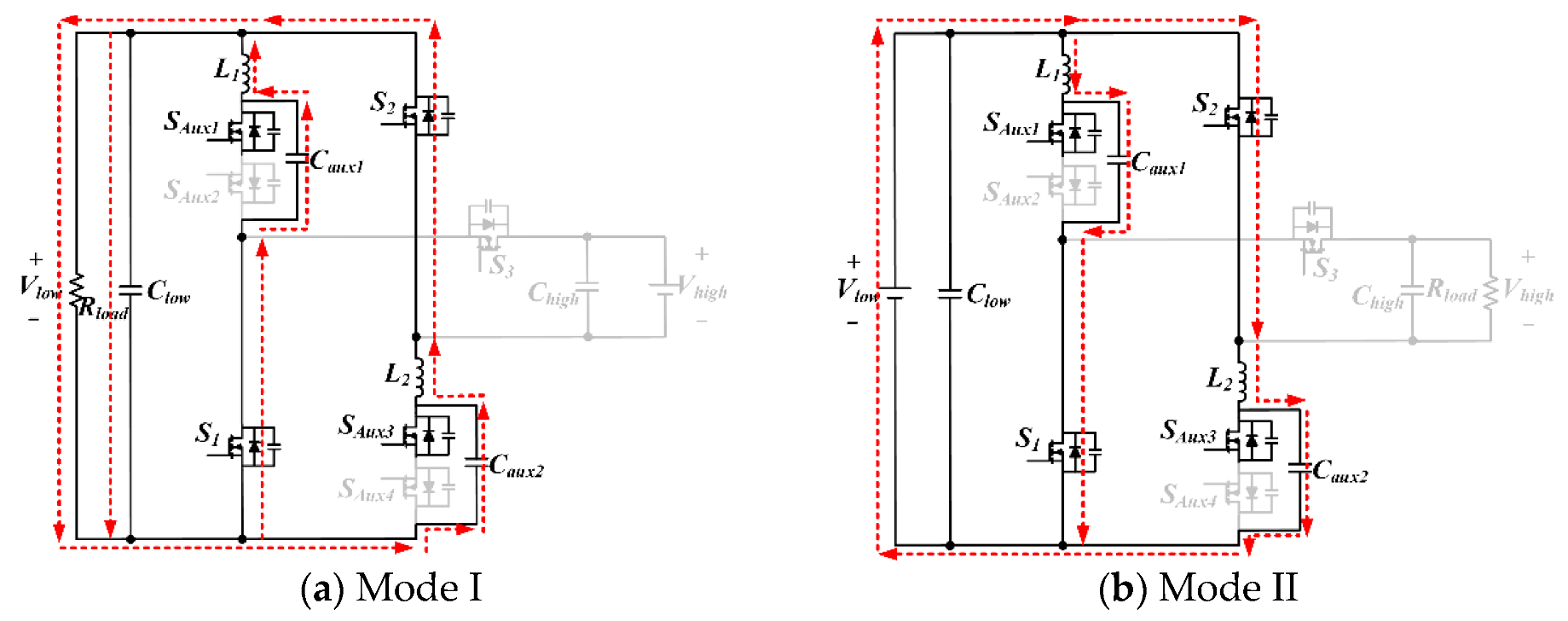
Step-Down to Step-Up Mode I (t0–t1)
Step-Down to Step-Up Mode II (t1–t2)
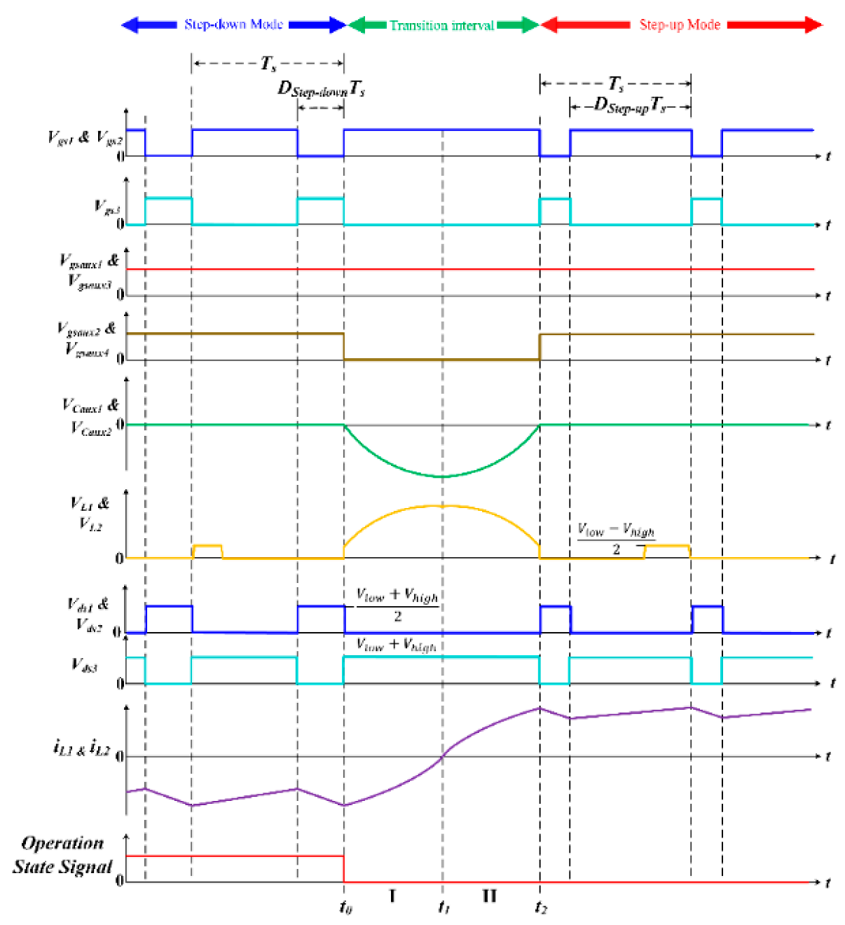
3.2. Transition Control Strategy
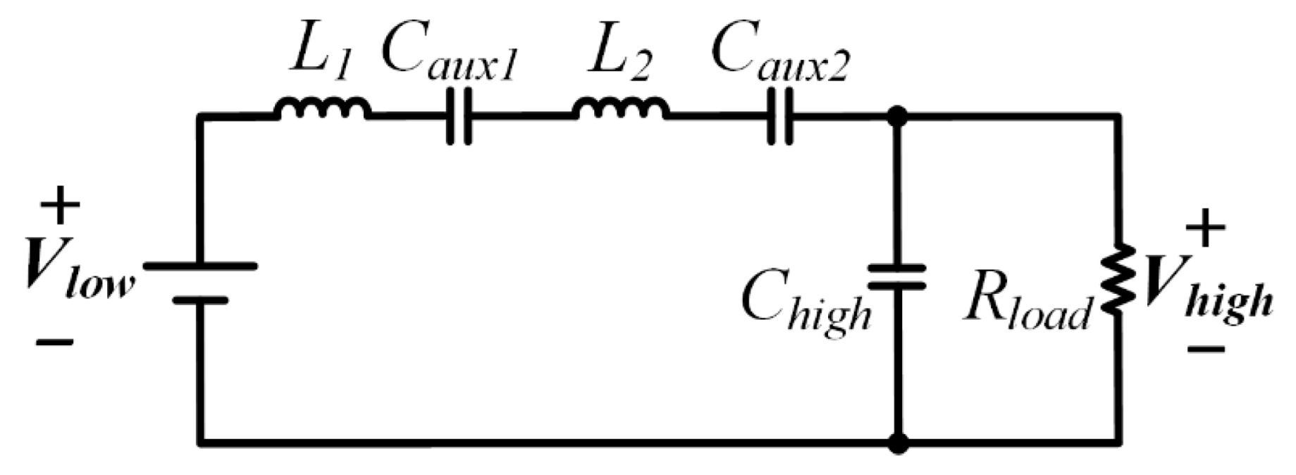
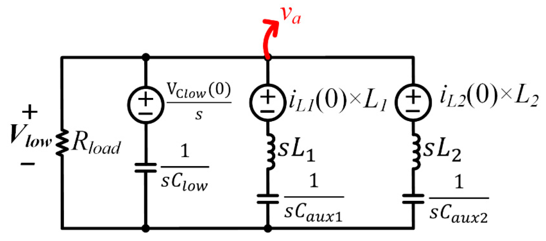
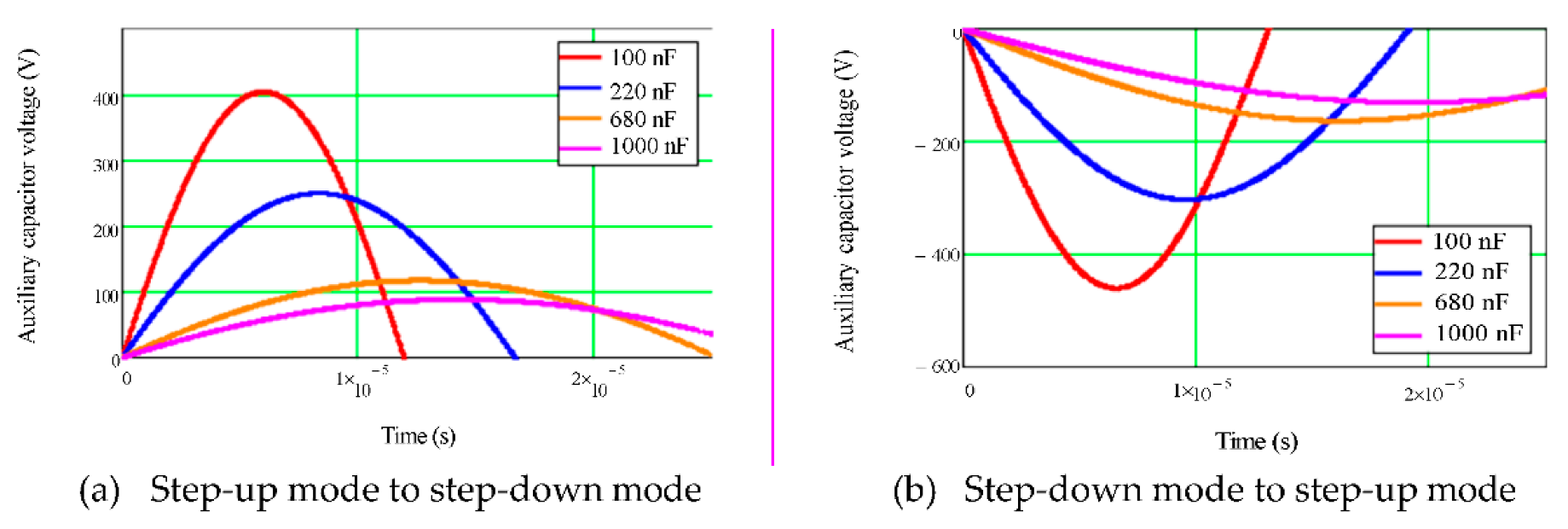
3.3. Component Parameter Design on Transient Interval
3.4. Component Design of Transition Technology
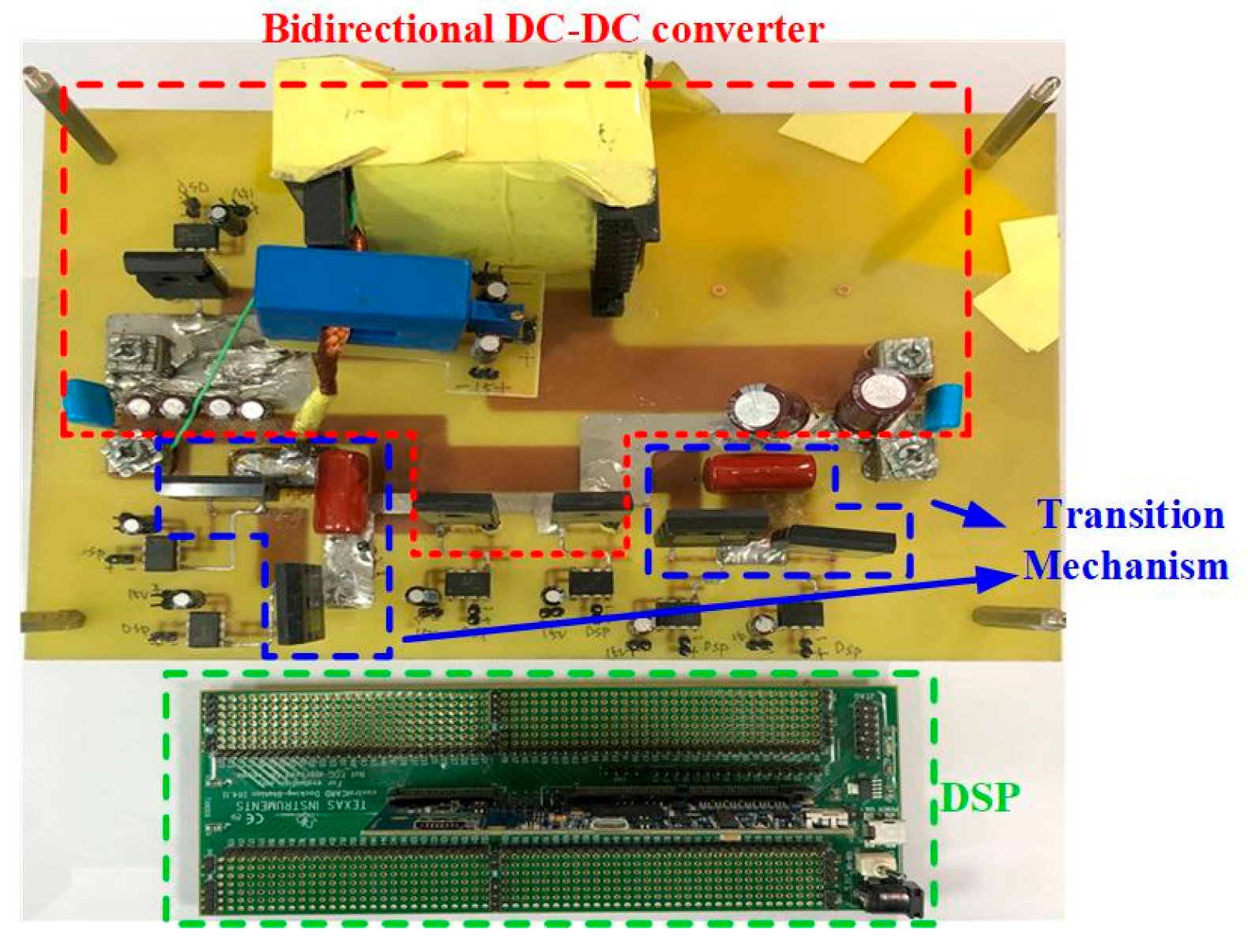
4. Experimental Results
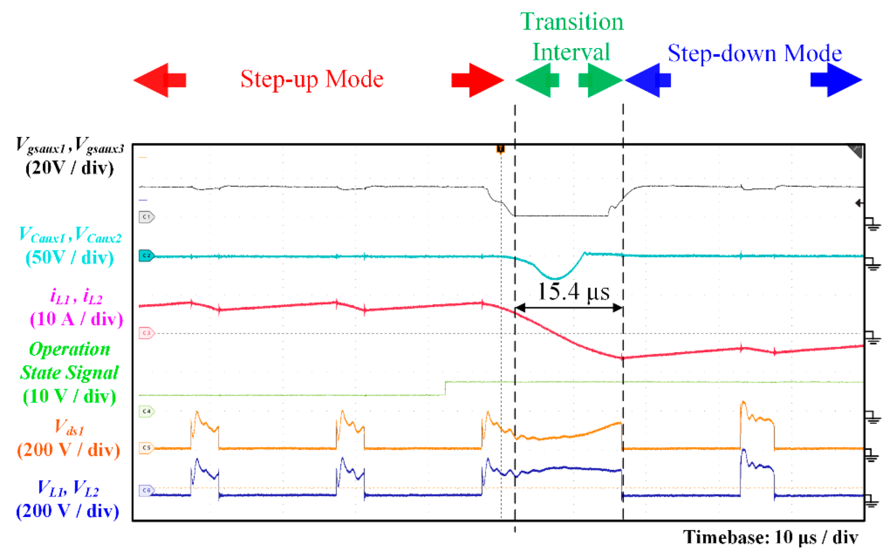
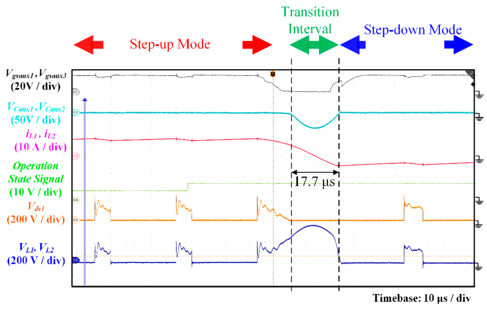
4.1. Step-Up Mode to Step-Down Mode in CCM Stage
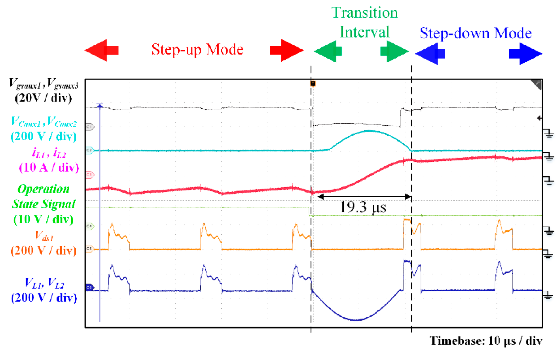
4.2. Step-Down Mode to Step-Up Mode in CCM
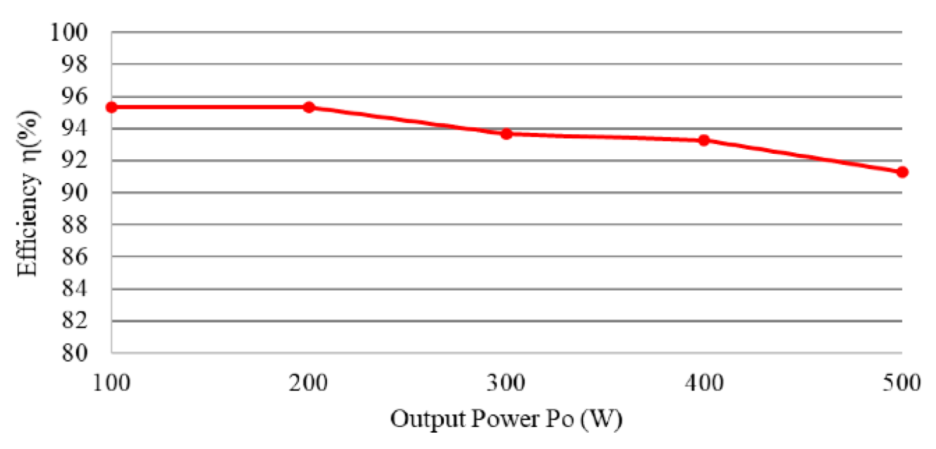
4.2.1. Efficiency in Step-Up Mode
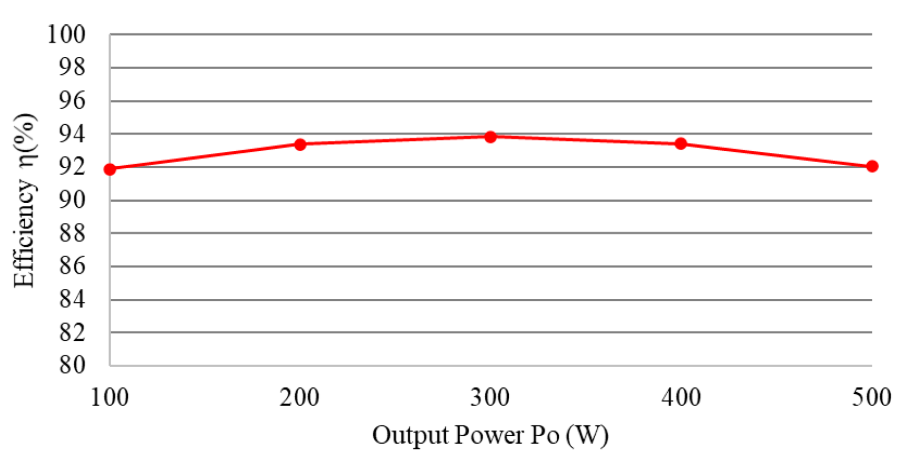
4.2.2. Efficiency in Step-Down Mode
4.2.3. Calculated Loss Distribution
5. Conclusions
Author Contributions
Funding
Conflicts of Interest
References
- Al-Shetwi, A.Q.; Hannan, M.A.; Abdullah, M.A.; Rahman, M.S.A.; Ker, P.J.; Alkahtani, A.A.; Mahlia, T.M.I.; Muttaqi, K.M. Utilization of Renewable Energy for Power Sector in Yemen: Current Status and Potential Capabilities. IEEE Access 2021, 9, 79278–79292. [Google Scholar] [CrossRef]
- Wu, C.; Zhang, X.-P.; Sterling, M.J.H. Economic Analysis of Power Grid Interconnections among Europe, North-East Asia, and North America with 100% Renewable Energy Generation. IEEE Open Access J. Power Energy 2021, 8, 268–280. [Google Scholar] [CrossRef]
- Elavarasan, R.M.; Shafiullah, G.M.; Padmanaban, S.; Kumar, N.M.; Annam, A.; Vetrichelvan, A.M.; Mihet-Popa, L.; Holm-Nielsen, J.B. A Comprehensive Review on Renewable Energy Development, Challenges, and Policies of Leading Indian States with an International Perspective. IEEE Access 2020, 8, 74432–74457. [Google Scholar] [CrossRef]
- Ahmed, S.D.; Al-Ismail, F.S.M.; Shafiullah, M.; Al-Sulaiman, F.A.; El-Amin, I.M. Grid Integration Challenges of Wind Energy: A Review. IEEE Access 2020, 8, 10857–10878. [Google Scholar] [CrossRef]
- Shafiullah, M.; Ahmed, S.D.; Al-Sulaiman, F.A. Grid Integration Challenges and Solution Strategies for Solar PV Systems: A Review. IEEE Access 2022, 10, 52233–52257. [Google Scholar] [CrossRef]
- Tang, Z.; Yang, Y.; Blaabjerg, F. Power electronics: The enabling technology for renewable energy integration. CSEE J. Power Energy Syst. 2022, 8, 39–52. [Google Scholar]
- Lu, X.; Guerrero, J.M.; Sun, K.; Vasquez, J.C. An improved droop control method for dc microgrids based on low band-width communication with dc bus voltage restoration and enhanced current sharing accuracy. IEEE Trans. Power Electron. 2014, 29, 1800–1812. [Google Scholar] [CrossRef] [Green Version]
- Khorsandi, A.; Ashourloo, M.; Mokhtari, H. A Decentralized Control Method for a Low-Voltage DC Microgrid. IEEE Trans. Energy Convers. 2014, 29, 793–801. [Google Scholar] [CrossRef]
- Strunz, K.; Abbasi, E.; Huu, D.N. DC Microgrid for Wind and Solar Power Integration. IEEE J. Emerg. Sel. Top. Power Electron. 2014, 2, 115–126. [Google Scholar] [CrossRef]
- Mahmood, M.S.; Mahmood, S. Cost effective optimal solution for hybrid power system among diverse sources of renewable energy. In Proceedings of the TENCON 2017—2017 IEEE Region 10 Conference, Penang, Malaysia, 5–8 November 2017; pp. 1214–1215. [Google Scholar]
- Pilz, M.; Al-Fagih, L. Recent Advances in Local Energy Trading in the Smart Grid Based on Game-Theoretic Approaches. IEEE Trans. Smart Grid 2019, 10, 1363–1371. [Google Scholar] [CrossRef] [Green Version]
- Xu, X.; Yan, Z.; Shahidehpour, M.; Wang, H.; Chen, S. Power System Voltage Stability Evaluation Considering Renewable Energy with Correlated Variabilities. IEEE Trans. Power Syst. 2018, 33, 3236–3245. [Google Scholar] [CrossRef]
- IEEE. 1668–2017—IEEE Recommended Practice for Voltage Sag and Short Interruption Ride-Through Testing for End-Use Electrical Equipment Rated Less than 1000 V; IEEE Std 1668–2017; Revision of IEEE Std 1668–2014; IEEE: Piscataway, NJ, USA, 2017. [Google Scholar]
- Tu, C.; Guo, Q.; Jiang, F.; Chen, C.; Li, X.; Xiao, F.; Gao, J. Dynamic Voltage Restorer with an Improved Strategy to Voltage Sag Compensation and Energy Self-Recovery. CPSS Trans. Power Electron. Appl. 2019, 4, 219–229. [Google Scholar] [CrossRef]
- Jiang, T.; Zhang, J.; Wu, X.; Sheng, K.; Wang, Y. A Bidirectional LLC Resonant Converter with Automatic Forward and Backward Mode Transition. IEEE Trans. Power Electron. 2015, 30, 757–770. [Google Scholar] [CrossRef]
- Callegaro, L.; Ciobotaru, M.; Pagano, D.J.; Turano, E.; Fletcher, J.E. A simple smooth transition technique for the noninverting buck-boost converter. IEEE Trans. Power Electron. 2018, 33, 4906–4915. [Google Scholar] [CrossRef]
- Tang, Y.; Chen, Y.; Madawala, U.K.; Thrimawithana, D.J.; Ma, H. A New Controller for Bidirectional Wireless Power Transfer Systems. IEEE Trans. Power Electron. 2018, 33, 9076–9087. [Google Scholar] [CrossRef]
- Xu, J. PWM modulation and control strategy for LLC-DCX converter to achieve bidirectional power flow in facing with resonant parameters variation. IEEE Access 2019, 7, 54693–54704. [Google Scholar] [CrossRef]
- Zhu, R.; Hoffmann, F.; Vázquez, N.; Wang, K.; Liserre, M. Asymmetrical bidirectional DC-DC converter with limited reverse power rating in smart transformer. IEEE Trans. Power Electron. 2020, 35, 6895–6905. [Google Scholar] [CrossRef]
- Kwon, M.; Choi, S. Control Scheme for Autonomous and Smooth Mode Switching of Bidirectional DC–DC Converters in a DC Microgrid. IEEE Trans. Power Electron. 2018, 33, 7094–7104. [Google Scholar] [CrossRef]
- Liserre, M.; Sauter, T.; Hung, J. Future energy systems: Integrating renewable energy sources into the smart power grid through industrial electronics. IEEE Trans. Ind. Electron. 2010, 4, 18–37. [Google Scholar] [CrossRef]
- Huang, A.Q.; Crow, M.L.; Heydt, G.T.; Zheng, J.P.; Dale, S.J. The future renewable electric energy delivery and management system: The energy internet. Proc. IEEE 2011, 99, 133–148. [Google Scholar] [CrossRef]
- Inoue, S.; Akagi, H. A bidirectional dc–dc converter for an energy storage system with galvanic isolation. IEEE Trans. Power Electron. 2007, 22, 2299–2306. [Google Scholar] [CrossRef]
- Tan, N.M.L.; Abe, T.; Akagi, H. Design and performance of a bidirectional isolated dc–dc converter for a battery energy storage system. IEEE Trans. Power Electron. 2012, 27, 1237–1248. [Google Scholar] [CrossRef]
- She, X.; Huang, A.Q.; Lukic, S.; Baran, M.E. On integration of solid state transformerwith zonal dcmicrogrid. IEEE Trans. Smart Grid 2012, 2, 975–985. [Google Scholar] [CrossRef]
- Babu, T.S.; Vasudevan, K.R.; Ramachandaramurthy, V.K.; Sani, S.B.; Chemud, S.; Lajim, R.M. A Comprehensive Review of Hybrid Energy Storage Systems: Converter Topologies, Control Strategies and Future Prospects. IEEE Access 2020, 8, 148702–148721. [Google Scholar] [CrossRef]
- Cornea, O.; Andreescu, G.; Muntean, N.; Hulea, D. Bidirectional Power Flow Control in a DC Microgrid through a Switched-Capacitor Cell Hybrid DC–DC Converter. IEEE Trans. Ind. Electron. 2017, 64, 3012–3022. [Google Scholar] [CrossRef]
- Ravi, D.; Reddy, B.M.; Letha, S.S.; Samuel, P. Bidirectional dc to dc Converters: An Overview of Various Topologies, Switching Schemes and Control Techniques. Int. J. Eng. Technol. 2018, 7, 360–365. [Google Scholar] [CrossRef] [Green Version]
- Gorji, S.A.; Sahebi, H.G.; Ektesabi, M.; Rad, A.B. Topologies and Control Schemes of Bidirectional DC-DC Power Converters: An Overview. IEEE Access 2019, 7, 117997–118019. [Google Scholar] [CrossRef]
- Swaminathan, N.; Cao, Y. An Overview of High-Conversion High-Voltage DC-DC Converters for Electrified Aviation Power Distribution System. IEEE Trans. Transp. Electrif. 2020, 6, 1740–1754. [Google Scholar] [CrossRef]
- Xu, Q.; Vafamand, N.; Chen, L.; Dragičević, T.; Xie, L.; Blaabjerg, F. Review on Advanced Control Technologies for Bidirectional DC/DC Converters in DC Microgrids. IEEE J. Emerg. Sel. Top. Power Electron. 2021, 9, 1205–1221. [Google Scholar] [CrossRef]
- Farhath, K.P.; Jayanand, B. Transformerless high step up dc-dc cascode converter with maximum power point tracking. In Proceedings of the 2015 International Conference on Power, Instrumentation, Control and Computing (PICC), Thrissur, India, 9–11 December 2015; pp. 1–6. [Google Scholar]
- Liu, W.-S.; Chen, J.-F.; Liang, T.-J.; Lin, R.-L.; Liu, C.-H. Analysis, Design, and Control of Bidirectional Cascoded Configuration for a Fuel Cell Hybrid Power System. IEEE Trans. Power Electron. 2010, 25, 1565–1575. [Google Scholar]
- Ho, C.N.; Chung, H.S.H.; Au, K.T.K. Design and implementation of a fast dynamic control scheme for capacitor supported dynamic voltage restorers. IEEE Trans. Power Electron. 2008, 23, 237–251. [Google Scholar] [CrossRef]
- Thummala, P.; Maksimovic, D.; Zhang, Z.; Andersen, M.A.E. Digital Control of a High-Voltage (2.5 kV) Bidirectional DC-DC Flyback Converter for Driving a Capacitive Incremental Actuator. IEEE Trans. Power Electron. 2016, 31, 8500–8516. [Google Scholar] [CrossRef] [Green Version]
- Chen, G.; Lee, Y.; Hui, S.; Xu, D.; Wang, Y. Actively Clamped Bidirectional Flyback Converter. IEEE Trans. Ind. Electron. 2000, 47, 770–779. [Google Scholar] [CrossRef]
- Qian, T.; Song, W.; Lehman, B. Self-Driven Synchronous Rectification Scheme for Wide Range Application of DC/DC Converters with Symmetrically Driven Transformers. In Proceedings of the IEEE Power Electronics Specialists Conference, Jeju, Korea, 18–22 June 2006. [Google Scholar]
- Ribeiro, E.; Cardoso, A.J.M.; Boccaletti, C. Fault Diagnosis in Non-isolated Bidirectional Half-bridge DC-DC Converters. In Proceedings of the IECON 2014—40th Annual Conference of the IEEE Industrial Electronics Society, Dallas, TX, USA, 29 October–1 November 2014; pp. 4458–4463. [Google Scholar]
- Odo, P. A Comparative Study of Single-phase Non-isolated Bidirectional DC-DC Converters Suitability for Energy Storage Application in a dc Microgrid. In Proceedings of the 2020 IEEE 11th International Symposium on Power Electronics for Distributed Generation Systems (PEDG), Dubrovnik, Croatia, 28 September–1 October 2020; pp. 391–396. [Google Scholar]
- Teng, J.; Chen, S.; Luan, S.; Xu, J. Bidirectional DC-DC Converter with a Wide-Range Voltage Conversion Ratio. In Proceedings of the 2019 IEEE 4th International Future Energy Electronics Conference (IFEEC), Singapore, 25–28 November 2019; pp. 1–6. [Google Scholar]
- Ahmad, A.; Beig, A.R.; Alsawalhi, J.; Jaafari, K.A. A Novel High Gain Bidirectional DC-DC Converter. In Proceedings of the 2020 IEEE Industry Applications Society Annual Meeting, Detroit, MI, USA, 10–16 October 2020; pp. 1–6. [Google Scholar]
- Mukhtar, N.M.; Lu, D.D.C. A Bidirectional Flyback Converter with Cross-Coupled Non-Dissipative Snubber Circuits. In Proceedings of the IEEE International Telecommunications Energy Conference, Broadbeach, QLD, Australia, 22–26 October 2017. [Google Scholar]
- Yang, L.; Liang, T. Analysis and Implementation of a Novel Bidirectional DC-DC Converter. IEEE Trans. Ind. Electron. 2012, 59, 422–434. [Google Scholar] [CrossRef]
- Yamamoto, K.; Hiraki, E.; Tanaka, T.; Nakaoka, M.; Mishima, T. Bidirectional DC–DC Converter with Full-Bridge/Push-Pull Circuit for Automobile Electric Power Systems. In Proceedings of the 37th IEEE Power Electronics Specialists Conference, Jeju, Korea, 18–22 June 2006. [Google Scholar]
- Chan, Y.P.; Loo, K.H.; Lai, Y.M. SVM-Plus-Phase-Shift Modulation Strategy for Single-Stage Immittance-Based Three-Phase AC-DC Bidirectional Converter. In Proceedings of the 19th European Conference on Power Electronics and Applications, Warsaw, Poland, 11–14 September 2017. [Google Scholar]
- Lin, B.R.; Chen, J.J.; Hsieh, F.Y. Analysis and Implementation of a Bidirectional Converter with High Conversion Ratio. In Proceedings of the IEEE International Conference on Industrial Technology, Chengdu, China, 21–24 April 2008. [Google Scholar]
- Elsayad, N.; Moradisizkoohi, H.; Mohammed, O.A. A new hybrid structure of a bidirectional DC-DC converter with high conversion ratios for electric vehicles. IEEE Trans. Veh. Technol. 2020, 69, 194–206. [Google Scholar] [CrossRef]
- Chen, B.Z.; Liao, H.; Chen, L.; Chen, J.F. Design and Implementation of the Bidirectional DC-DC Converter with Rapid Energy Conversion. Energies 2022, 15, 898. [Google Scholar] [CrossRef]


| Step-Up Mode | Step-Down Mode | ||
|---|---|---|---|
| Low-side voltage, Vlow | 24 V | High-side voltage, Vhigh | 200 V |
| High-side voltage, Vhigh | 200 V | Low-side voltage, Vlow | 24 V |
| Output power, Pset-up | 500 W | Output power, Pset-down | 500 W |
| Switching frequency, fs | 50 kHz | Switching frequency, fs2 | 50 kHz |
| Item | Value |
|---|---|
| Inductors L1, L2 | 185 μH |
| Capacitor Clow | 35 μF/35 V |
| Capacitor Chigh | 22 μF/250 V |
| Auxiliary capacitor Caux1, Caux2 | 220 nF/600 V |
| Main switches S1, S2, S3 | IMW65R048M1H (650 V/39 A/48 mΩ) |
| Auxiliary switches SAux1, SAux2, SAux3, SAux4 | SCTWA90N65G2V-4 (650 V/119 A/24 mΩ) |
| Digital signal processor (DSP) | TMS320F28379D |
| Item | Equation |
|---|---|
| S1 | |
| S2 | |
| S3 | |
| Saux1 & Saux2 & Saux3 & Saux4 | |
| L1& L2 |
Publisher’s Note: MDPI stays neutral with regard to jurisdictional claims in published maps and institutional affiliations. |
© 2022 by the authors. Licensee MDPI, Basel, Switzerland. This article is an open access article distributed under the terms and conditions of the Creative Commons Attribution (CC BY) license (https://creativecommons.org/licenses/by/4.0/).
Share and Cite
Liao, H.; Chen, Y.-T.; Chen, L.; Chen, J.-F. Development of a Bidirectional DC–DC Converter with Rapid Energy Bidirectional Transition Technology. Energies 2022, 15, 4583. https://doi.org/10.3390/en15134583
Liao H, Chen Y-T, Chen L, Chen J-F. Development of a Bidirectional DC–DC Converter with Rapid Energy Bidirectional Transition Technology. Energies. 2022; 15(13):4583. https://doi.org/10.3390/en15134583
Chicago/Turabian StyleLiao, Hsuan, Yi-Tsung Chen, Linda Chen, and Jiann-Fuh Chen. 2022. "Development of a Bidirectional DC–DC Converter with Rapid Energy Bidirectional Transition Technology" Energies 15, no. 13: 4583. https://doi.org/10.3390/en15134583
APA StyleLiao, H., Chen, Y.-T., Chen, L., & Chen, J.-F. (2022). Development of a Bidirectional DC–DC Converter with Rapid Energy Bidirectional Transition Technology. Energies, 15(13), 4583. https://doi.org/10.3390/en15134583