1. Introduction to the Subject Matter
Modern sea-going ships are autonomous objects in terms of energy, with limited resources of energy and power. At present, an increasing number of ships are being equipped with electric propulsion systems powered by a diesel engine, and much less frequently by a package of batteries. Newbuilds with electric high-power main propulsion generally utilize synchronous motors, installed for example in podded propellers [
1]. From the power electronic perspective, they are controlled and powered by current and voltage converters. Semiconductor elements utilized in power electronic converters include half-controlled thyristors (SCR), gate turn-off (GTO) and integrated gate-controlled thyristors (IGCT), or an integrated gate bipolar transistor (IGBT), and injection-enhanced gate transistor (IEGT). The power range offered and already installed in electric main propulsion exceeds 20 MW, which requires an increasingly higher voltage of marine power plants; up to 15 kV. At the same time, attempts are being made to employ greater currents of conduction at lower losses, higher reverse voltages, and better dynamic properties (higher frequencies of switching) [
2,
3].
The lifetime of a power electronic system depends on the characteristics of system components such as capacitors, gate drivers, insulated gate bipolar transistors, etc., [
4,
5]. Among them, the IGBT is the main component that affects the life of the entire system. The current flowing through the IGBT determines the temperature variation, and the failure of the transistor structure depends on the thermal behavior [
6,
7,
8]. Variations in junction temperature cause repetitive thermomechanical stresses in the IGBT module, which accumulate as fatigue on the device [
5,
9,
10].
The failure of the bond wire distorts the current flowing to the IGBT module and accelerates the lifting of bond-wire liftoff and the tearing of the remaining bond wire [
11]. These failures can lead to a no-load failure or catastrophic failure of switching devices, such as thermal runaway and damage to semiconductor chips. Furthermore, temperature fluctuations can lead to solder joint fatigue [
11,
12]. A standard IGBT module has two solder joints: between the IGBT chip and the direct bond copper substrate (DBC) and between the DBC substrate and the ground plane. Thermomechanical stresses are applied to the solder joints due to changes in the coefficient of thermal expansion caused by temperature changes, thereby degrading the solder interface, such as B, which can cause cracks and delamination.
2. Marine Power Electronic Switching Systems
The need to find a solution of a switch and signal amplifier that works faster with smaller conduction losses and is relatively simple to fabricate, brought considerable progress in the research of IGBT transistors. In high power drives, the frequencies of IGBT switching oscillates between 1 kHz and 3 kHz. An increased frequency of switching reduces the current and unwanted voltage harmonics as the voltage waveform becomes closer to the sinusoidal, increasing the frequency of switching results in greater losses, and consequent heating of the semiconductor element.
In power electronic propulsion systems, particularly in specialized ships or drilling platforms, high reliability and protection of all critical infrastructure equipment are required. These critical units include propeller systems, positioning systems drilling and production processes, and a few significant others.
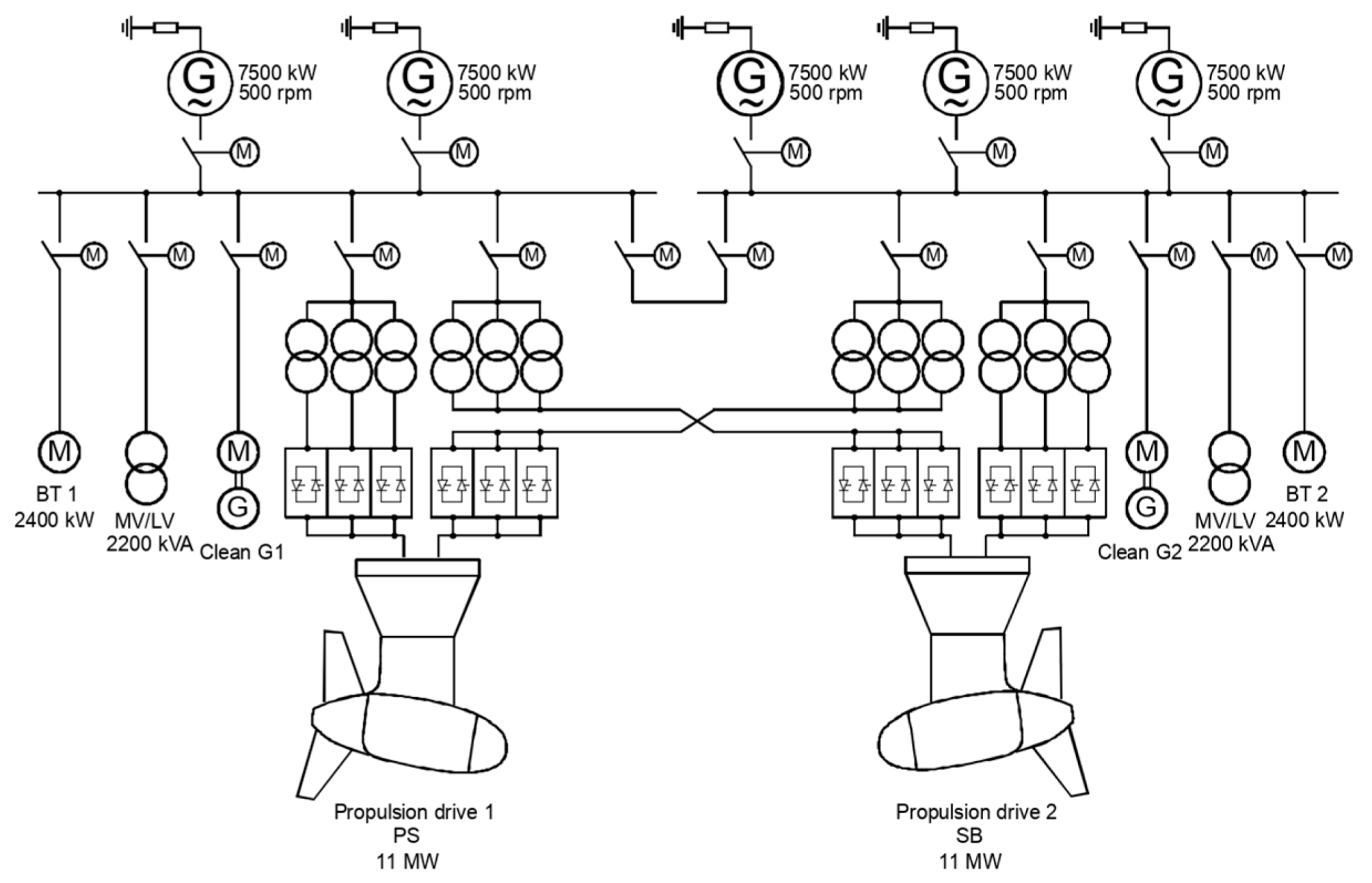
A typical topology of a propulsion system equipped with podded propellers powered by power electronics converters is provided in
Figure 1. How important the diagnostics of electronic power converters is can be seen by how many ship devices are handled. In this example drawing (
Figure 1) there are two large electric rotary thrusters (PS, SB), they are just driven by electronic power converters. Although the system is redundant, any failure entails the risk of losing control or drive. In addition to the main drive, electronic power devices are often used by voltage generators (G) (voltage and current stabilizing inverters). Moreover, we work with numerous devices powered by engines of various types (M), e.g., fans, mooring forks, unloading cranes, and fuel centrifuges.
Although most critical marine power electronics devices are doubled, i.e., at least one identical system is installed in parallel, allowing instant switching to take over the load, the specific conditions lead engineers to seek even higher reliability of electronic systems in use. Difficult working conditions of these devices are an additional factor increasing the research problem. The harsh marine environment (high humidity and salt content in the atmosphere) also affects the failure rate of the systems.
The possibility of diagnosing the above modules or anticipating the condition of devices is an essential problem from economic and safety perspectives raised by many operators.
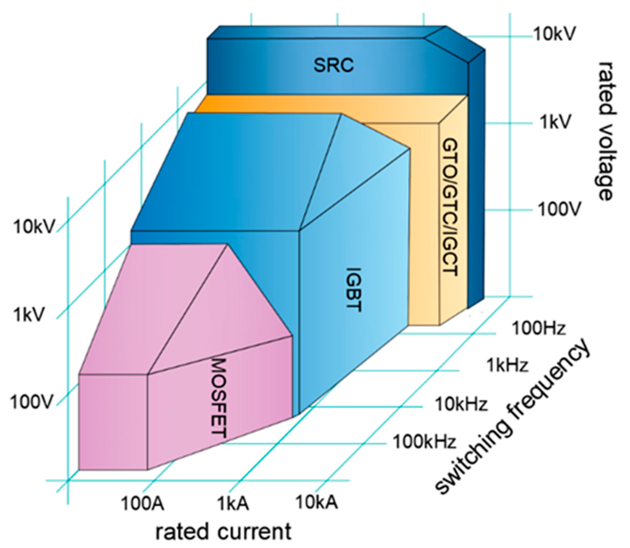
Figure 2 presents the range of marine power electronic system parameters [
3,
12].
An analysis of the operational range of marine power electronic instruments shown in
Table 1 indicates clearly that these factors are an important element of marine converting devices.
IGBT transistors are commonly used in ship propulsion power electronics systems, medium power converters and power management control systems, and active filters in compensation systems.
In
Table 1 and
Figure 2, the authors omitted SiC-based transistors. It is true that they have better parameters than IGBTs and can be switched at higher frequencies, but due to the existing industrial applications, IGBT transistors require diagnosing and forecasting of their technical condition.
There is a growing need to investigate the ability to diagnose semiconductor circuits during operation, such as in marine use. In [
13], the effect of the off current on the low- and high-frequency components of the generated internal acoustic emission wave was investigated. The low-frequency component has a linear relationship with the turn-off current, and the switch part can accurately follow the change in the turn-off current, indicating that the low-frequency component has a strong correlation with the turn-off current. The study presented here confirms results related to the use of acoustic emission signals in IGBT transistors. Evaluating the stability and operation of IGBTs by measuring saturation voltage drop, reverse current, and turn-off time as measurement parameters was proposed in [
11].
A comparative study of the junction temperature variation in SiC-based MOSFETs and silicon-based IGBTs and photovoltaic inverter applications, as well as the junction temperature of semiconductors which can determine and compare the thermal constraints of SiC MOSFETs and silicon-based IGBT power modules, was shown in [
14]. The presence of electromagnetic interference in the AE measurement and its contribution to the signal obtained in the GTO thyristor is shown in [
15].
3. Power Electronics Modules and Their Properties
Power modules are generally designed and produced so that they meet the typical operational and service life requirements. Following technical requirements (e.g., electric, thermal, mechanical, costs, dimensions, etc.) one typically attempts to solve the problem by using one objective of optimization, i.e., the maximization of IGBT modules lifetime when only one specific failure is considered. In practice, the IGBT module is usually subject to combined effects of vibrations, fatigue, and temperature.
Third generation IGBT transistors allow the junction to work in higher temperatures. Commonly, catalogue data indicate a working range up to 150 °C. This is essential due to problems with heat transfer and dissipation. Thermal resistance between the junction and the housing is similar in MOSFET transistors (in the same kind of case), which results from the similarity of the semiconductor structure. The temperature impact on all electrical parameters is also important so the manufacturers must provide an efficient way to cool semiconductor structures.
Table 2 presents various failure mechanisms of the IGBT module. As it is shown in [
5,
10], temperature issues (T and ΔT) are the main cause of power electronics device damage.
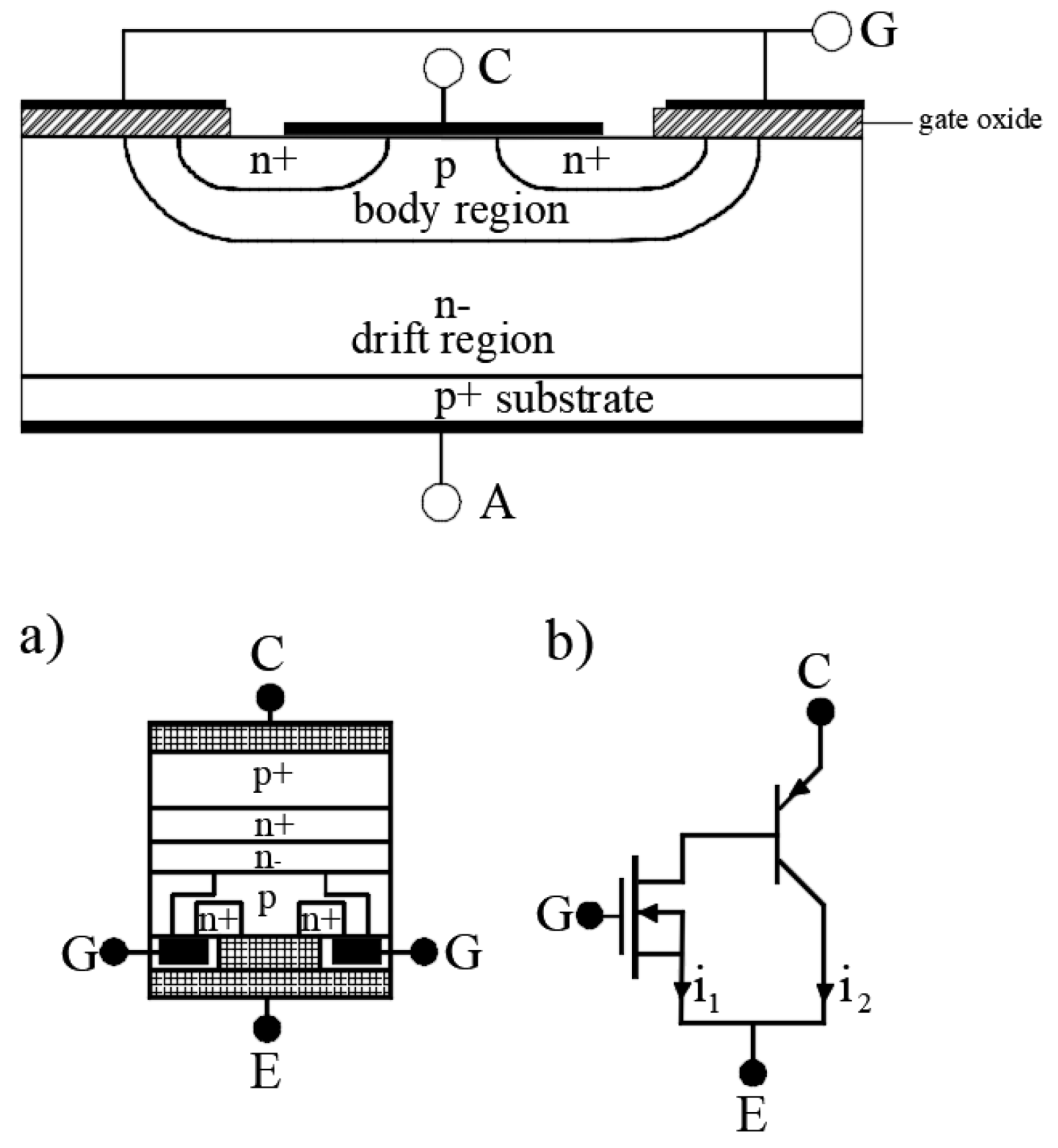
Bipolar transistors show a negative voltage saturation coefficient (MOSFET transistor-positive resistance coefficient of the switched-on channel). For an IGBT, the temperature coefficient of this parameter is close to zero while slightly negative in the low current area and slightly positive in high currents. The most important, however, is the conclusion that IGBT transistors of the same type and parameters can be connected to work in parallel. These transistors are also more resistant to destruction due to thermal runaway, as no current density concentration occurs in the ‘hotter’ area of the transistor channel. IGBTs also do not have a parasitic connection, forming an ‘anti-parallel’ diode. Depending on the application, this can act as an advantage or drawback of a structure. Usually, the semiconductor switch works in the circuits of commutation with inductive load. Such a diode is required to recover energy collected in inductance when the transistor is in the off-state. In the case of IGBT switches, an external freewheeling, fast recovery diode is required.
The reliability of the IGBT transistor depends, inter alia, on well-devised protection circuits. Practically every failure of a device working in the switch mode results in a failure of the switching component. The IGBT transistor is a voltage-controlled element. From an electrical point of view, it can be roughly stated that the gate circuit represents capacitance, and this parasitic parameter should be examined for possible transistor failure. The capacitance is not constant and contributes to the emitter-gate and gate-collector junctions. The former should be quickly recharged due to fast control, while the latter is the cause of the negative feedback phenomena which additionally slows down the process of gate overcharging.
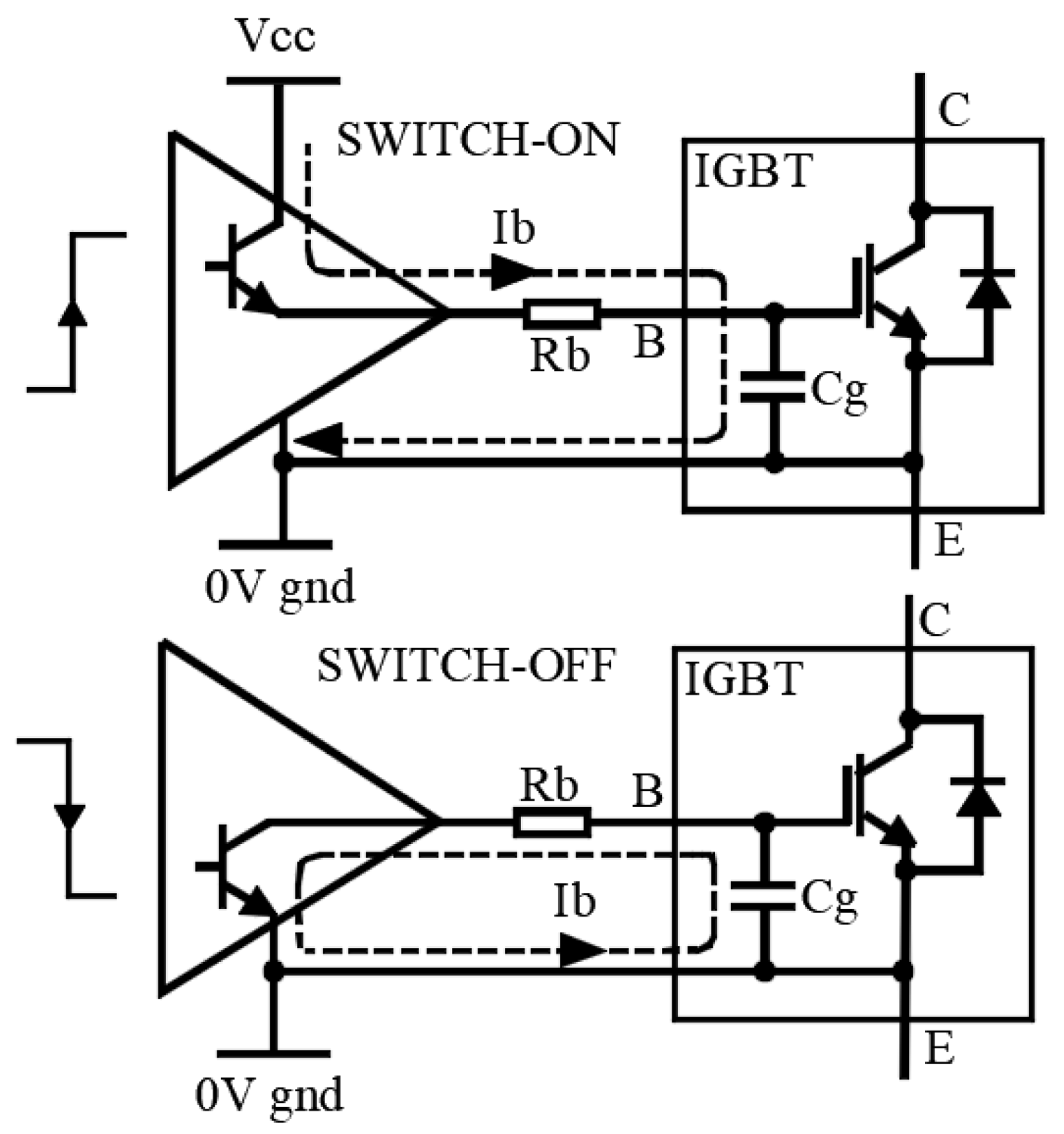
In the case of high current switching at relatively significant frequencies, gate driving is quite a complicated process. With mid to high switching frequencies due to internal parasitic capacitance, gate currents can be notably high within a wide voltage range. To optimize the control process, the voltage source along with resistance in the gate circuit can be applied, which is shown in
Figure 3.
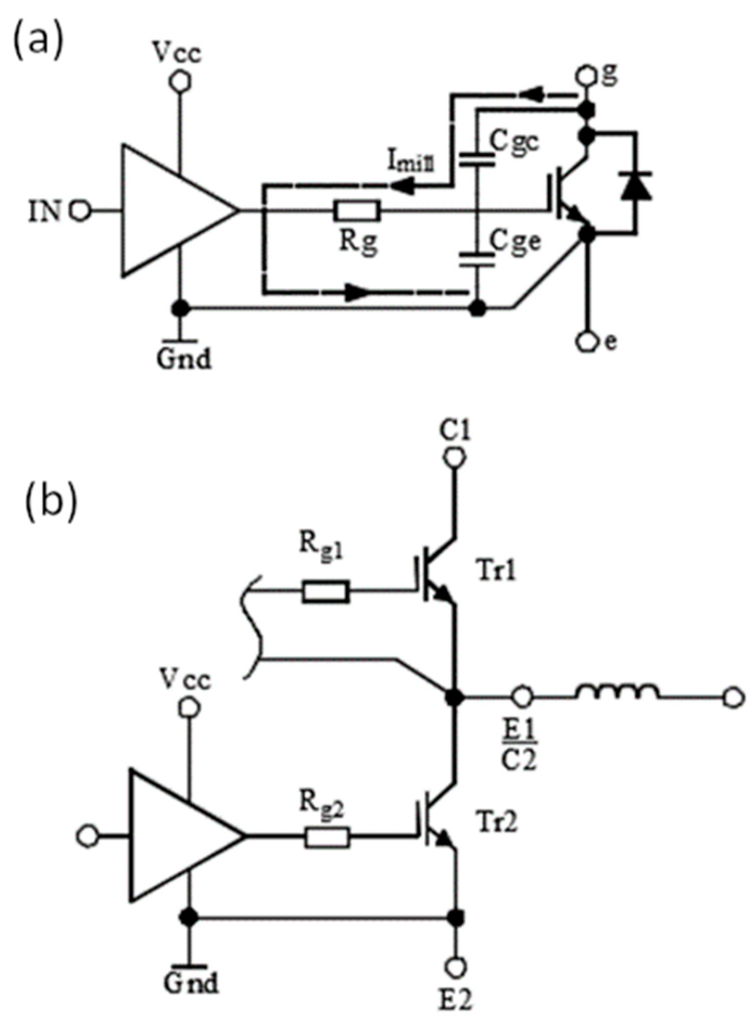
The presence of negative voltage is usually a problem. Practice shows that in collector currents up to 100 A, negative voltage is practically not present. Manufacturers catalogs usually provide strict recommendations in this respect, while the resultant driver is the simplest possible one (
Figure 4). However, there are at least two problems here. One is the presence of capacitance between the gate and collector, known as Miller capacity, due to the Miller effect of this capacitance.
This is an effect of local negative feedback, which slows down the switching process. Moreover, transistors switches in high power circuits usually work in pairs utilizing bridge or half-bridge configurations. In such cases, turning off one transistor may cause false switching on the other due to Miller capacitance. Cgc forms a divider along with Rg. If the voltage on this divider exceeds the threshold level of gate voltage, the transistor turns on; the risk of unwanted firing up of the transistor increases as temperature rises because in such conditions the threshold level slightly decreases.
That is the main reason the lowest possible values of resistance Rg should be used to prevent this phenomenon and when this is insufficient, the negative voltage should be used. This is one of the practical conclusions resulting from the mentioned theory. A similar risk providing the same effect inevitably results from the parasitic inductance present in the transistor emitter structure, particularly significant for currents reaching hundreds of amps and pulse steepness expressed in kV/μs. Even when the transistor is switched off, considerable currents can flow, recovering energy through freewheeling diodes. The dI/dt in the circuit of one key is transferred to the circuit of the other, inducing negative voltage on its emitter. The result may be similar: false turn-on of an IGBT transistor which may suffer damage because of uncontrolled current flow. Proper assembly is essential in this context. Therefore, in high power circuits, the reference potential of the driver should be directly connected to the transistor emitter that it controls.
Similarly, to obtain protection from damage due to inductance in the collector circuit, so-called snubber circuits are used. The transistor can also be protected by local feedback from the collector to the driver. However, one should expect greater power losses in the semiconductor switch, so this kind of safeguard has limited applications. Another type of protection is a short circuit that monitors the voltage of the collector (sometimes the emitter current is measured). When the transistor is out of saturation, after a delay of a few microseconds, it turns off the transistor excluding damage due to very high energy emitted in the collector circuit. This type of protection also prevents the transistor from experiencing the latch-up effect.
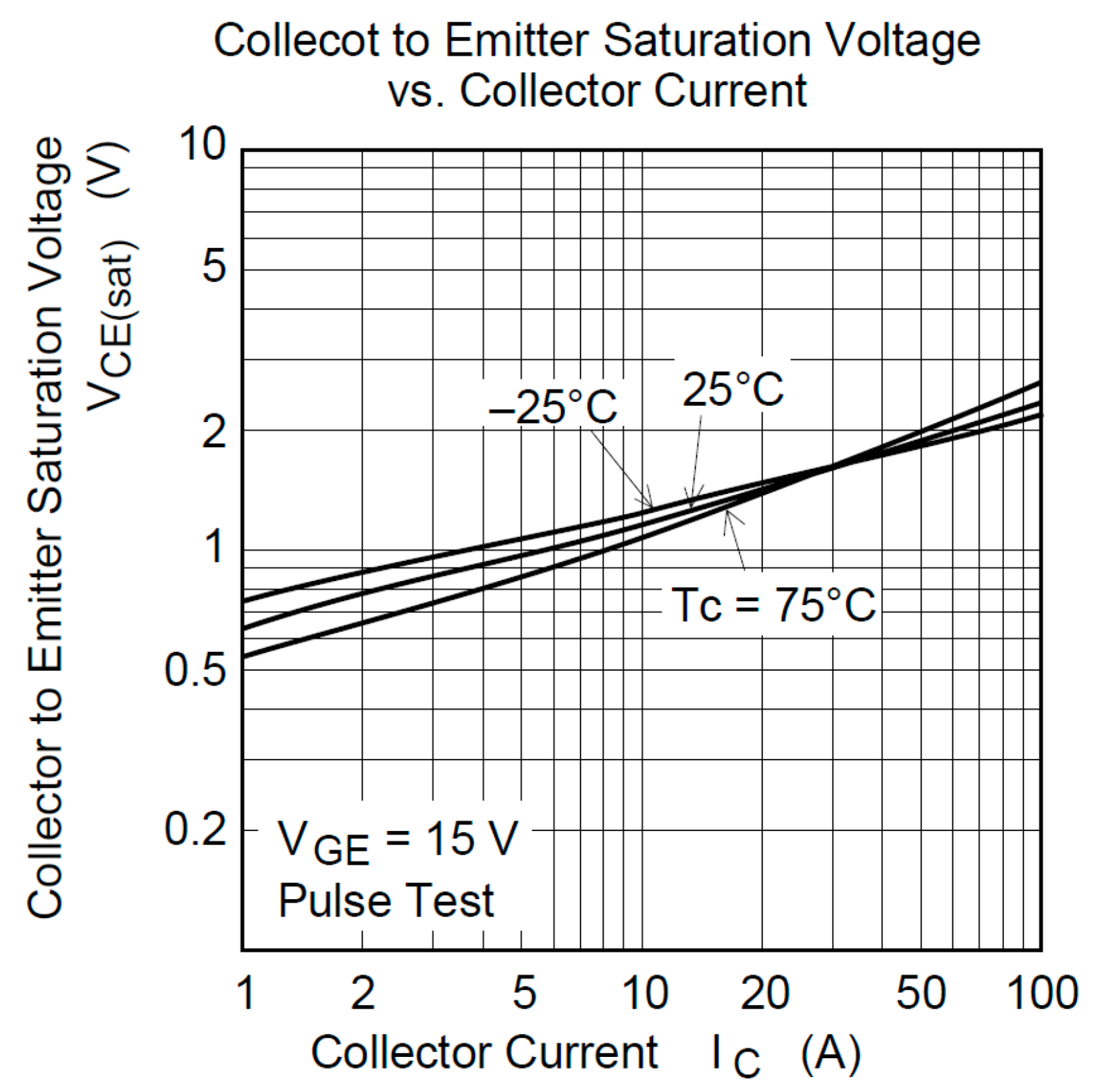
It should be noted that 3rd generation IGBT transistors (Trench-Field-Stop IGBT) do not show as many losses of power as IGBT1 and IGBT2. They show a shorter-lasting ‘current tail’ in the turning-off stage and slightly lower saturation voltage. IGBT transconductances are generally higher than those of MOSFET transistors. In the working component, the essential relationship is between temperature and saturation voltage (
Figure 5). In a low range of collector current, the temperature coefficient is negative (such as for BJT) in the high current range.
The saturation voltage Vce as a function of the current changes almost linearly. As the temperature changes, the slope of the plotted line changes. Near the rated current (in
Figure 5—30 A) the lines intersect. The measurements were carried out with the gate emitter voltage Uge equal to 15 V. In all cases, when the current flowing through the collector increases, the voltage drop across Uce increases, which is inadvisable as the power lost on the transistor increases.
4. Description of the Research Object
Because IGBT transistors have a strictly specific range of allowable working temperatures, the authors focused on seeking diagnostic relationships that can be used in monitoring the conditions where the transistor is close to the maximum working temperature.
One of the tested objects was a voltage source inverter (VSI). VSIs are mainly used with electric induction motors, but can also be used for synchronous machines, including permanent magnet motors. At present, the power of propulsion fed by VSI is limited to 8–10 MW due to available power electronics elements that can work at high frequency. The most often used method of inverter control is pulse width modulation (PWM) and space-vector sensorless control where the inverter switches work in the frequency ranging from 1 to 20 kHz. In marine high power propulsion systems, the switching frequency of IGBT transistors is approximately 1 kHz to minimize switching losses and heat emission. It is known that with increasing of inverter switching frequency the electric motor current is similar to a sinusoid; however, switching losses (mainly on heat) increase [
3,
12].
The transistor working conditions, i.e., values of constant voltage polarizing the base-emitter and base-collector junctions without the presence of a variable input signal, determine how the transistor responds to a variable input signal. The bipolar junction transistor demonstrates current gain, IGBT is a transconductive element; the input parameter is the gate voltage, and the output signal is the collector current (
Figure 6).
The measurement circuit of the transistor tested in laboratory conditions is shown in
Figure 7.
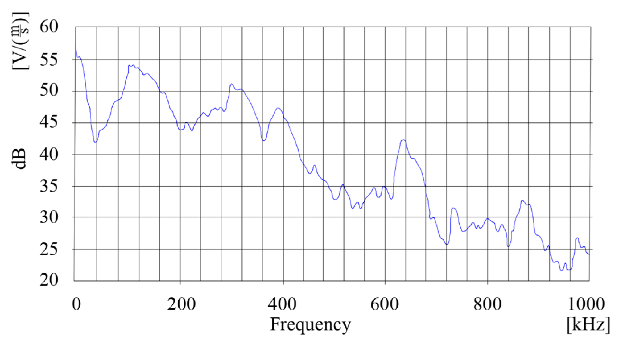
The measurement circuit utilizes a wideband acoustic emission WSα sensor from the Physical Acoustic Corporation (MISTRAS) characterized by high sensitivity and the wideband frequency range shown in
Figure 8. Broadband AE sensors are useful when frequency analysis of AE signals are required and the dominant frequency bands of AE sources are determined for noise discrimination and selection of suitable low-cost general-purpose AE sensors. In high-fidelity applications, broadband sensors can detect different AE wave patterns, providing more information about the AE source and the distance to the AE event. The 30° angle of the bottom edge of the sensor cavity reduces the risk of short circuits from the sensor cavity to the conductive test surface. The wide frequency response of the WS alpha sensor is not linear over the entire range. Its sensitivity drops with increasing frequency, as seen in
Figure 8. The decrease in sensitivity expressed in V/(m/s) is not linear and depends on the characteristics of the piezoelectric used in the sensor.
The signal was recorded using an AE recorder designed at the Maritime University of Szczecin, and additionally, the measurement results were confirmed by a two-channel AE recorder from the MISTRAS (Pocket AE-2).
A series of measurements were performed for various parameters, these measurements confirmed the thesis that with increasing temperature, the AE acoustic emission measured on the transistor’s housing has a lower amplitude. Only selected results are presented in the article. In the measurements, apart from temperature, the current was switched by the transistor, the frequency with which the transistor was used was switched, and the voltage with which the transistor was used was switched.
5. The Experimental Results
As indicated earlier, the effect of temperature is an important indicator to identify the state of the transistor. During the tests, the authors confirmed the influence of the transistor’s working temperature on its amplitude-frequency spectrum of acoustic emission signals. The narrow range of ‘safe temperatures’ was considered. By safe temperature, we mean a temperature that does not directly affect the damage of the component. The authors sought to identify direct relationships between temperature rise and the acoustic emission signal emitted. The tests were conducted with temperature increases from 25 °C to 75 °C (10 °C increments). Due to the limited volume of this paper, the results are provided for 25 °C, 45 °C, and 75 °C. The AE time signal clearly indicates the pulse of the transistor switching (
Figure 9). As mentioned earlier, by analyzing the catalog data of bipolar transistors, it can be seen that the maximum allowable operating temperature of these components should not exceed 150 °C. To investigate whether there is any temperature dependence of the emitted AE signal, an amplitude-time-frequency analysis was performed for increasing temperatures. The results indicate that a higher operating temperature of the transistor generates additional AE waves in the frequency band characteristic of transistor operation (
Figure 10).
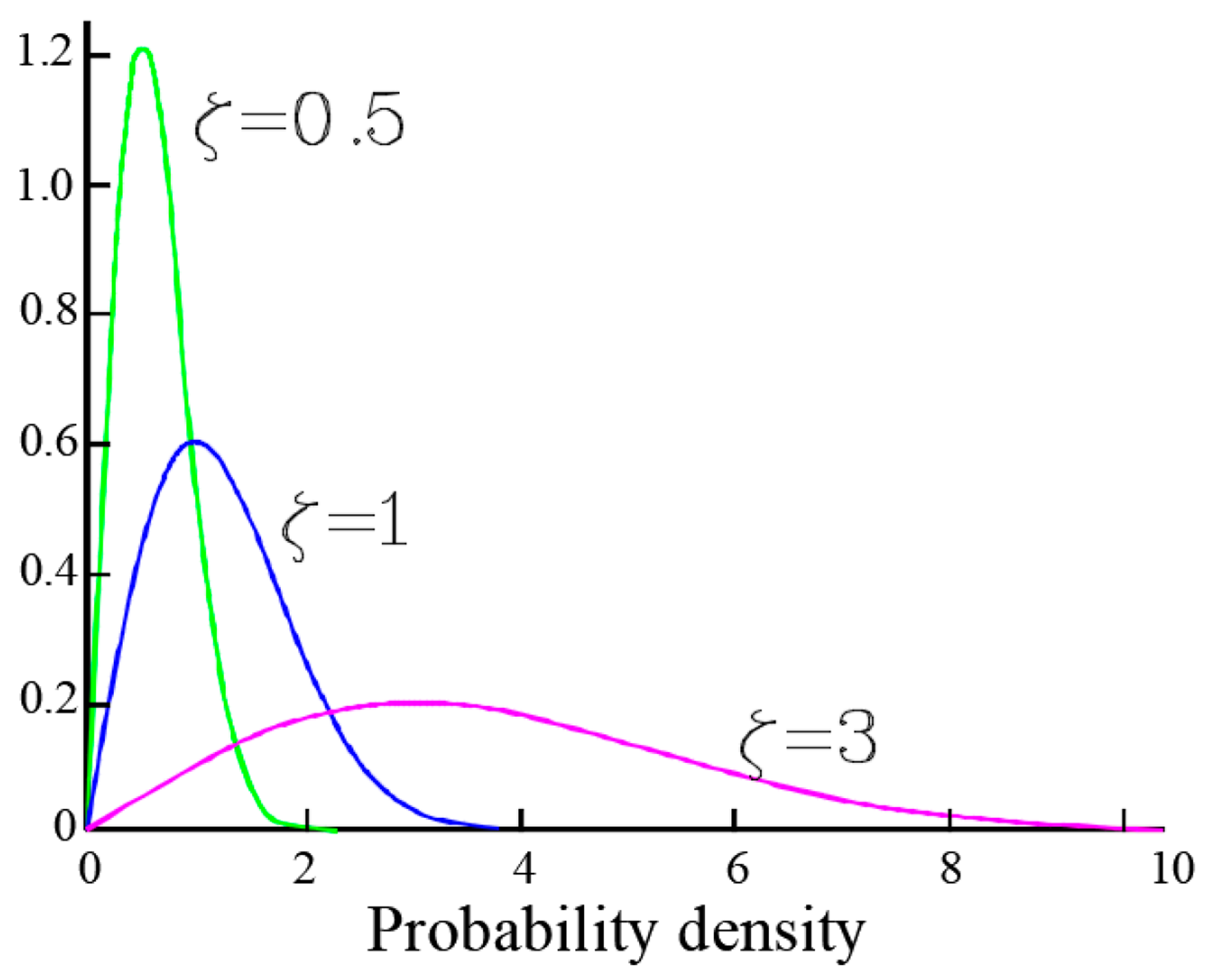
In the case of discrete acoustic emission (during transistor switching), the theoretical Rayleigh distribution can be used where the frequency of the occurrence of event rate
Nz for maximum signal amplitudes
Am can be written as:
where
ζ is the maximum value of the threshold of discrimination
A, and
Nc is the total rate of events of various amplitude.
The
Nz is a Rayleigh distribution with a shape forming parameter
ζ. The probability density function for different shape parameters
ζ is shown in
Figure 11. The three values of the parameter
ζ are shown because it is sufficient to graphically show how this parameter affects the probability density function.
The distribution of the event rate of any amplitude for expression (1) can be determined by integrating this expression relative to Am.
Assuming the curves of amplitude distribution of the event rate, it is possible to approximate these curves with the power function:
where
are the empirically chosen constants.
The tests were performed with the same current-voltage parameters. The only variable value was the temperature of the board on which the IGBT transistor was mounted.
Figure 12 shows the results of wavelet analyses for selected operating temperatures of IGBT transistors (sequentially as in
Figure 11).
In the range of increasing temperatures, a decrease in the signal amplitude can be clearly seen. This is caused by the increase in the ambient temperature; there is a smaller jump in the temperature of the semiconductor and thus the elastic wave has a smaller amplitude. At the same time, the wavelet decomposition is interesting, whereas the transistor temperature increases, the frequency components are decomposed into two bands (
Figure 12). As the temperature increases, in addition to the apparent peak associated with transistor switching, additional waveform signals appear, generating frequency gains that depend on the operating temperature of the transistor.
