
Multiple Input Multiple Output Resonant Inductive WPT Link: Optimal Terminations for Efficiency Maximization

 ,
,  ,
,  ,
, 
Abstract
1. Introduction
2. Power Gain Maximization for a Lossy Reciprocal Multiport Network
2.1. Statement of the Problem
2.2. Solving the Generalized Eigenvalue Problem
2.3. Calculation of the Optimal Terminating Networks and
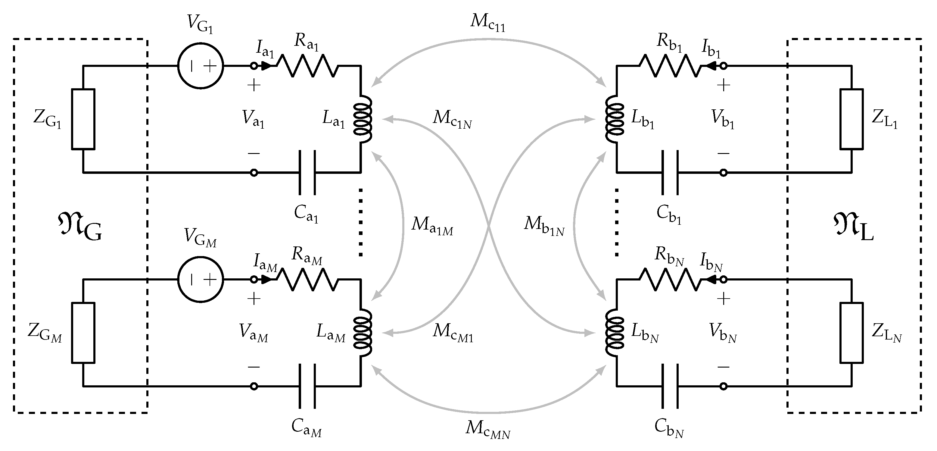
3. The Case of a Resonant Inductive WPT Link
4. MISO and SIMO Cases
4.1. MISO: 2TX 1RX
- the optimal currents at the transmitter side are orthogonal to the current at the receiver’s end;
- by adding a transmitter, is increased and the maximum gain is also increased;
- the optimal load value depends on the coupling with both generators through and is increased when we add a second transmitter;
- the optimal generators’ impedances and voltages depend on the coupling of the load with both generators, while the coupling between the two generators () only affects the reactive part.
4.2. SIMO: 1TX 2RX
- the optimal currents at the receiver side are orthogonal to the current at the transmitter’s end;
- by adding a receiver, is increased and the maximum gain is also increased;
- the value of the optimal generator impedance depends on the coupling with both loads through and is increased when we add a second receiver;
- the optimal voltage to be provided by the generator depends only on the coupling of the generator with both loads, it is independent of the coupling between the two loads;
- the real parts of the optimal load impedances depend only on the coupling of the generator with both loads, while the coupling between the two loads () only affects the reactive parts.
5. Validation
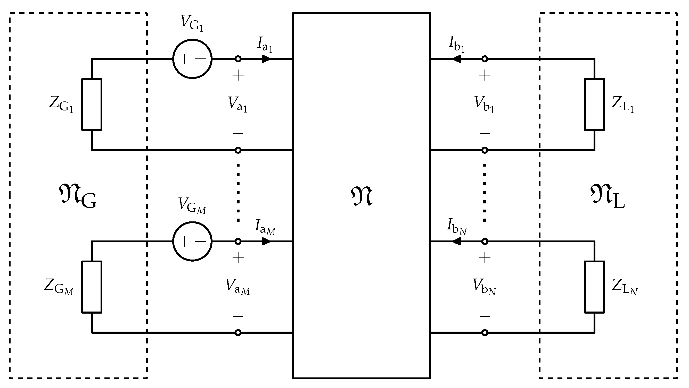
- consider the ports where the generators will be connected and the ports where the loads will be connected, number the ports of the network as illustrated in Figure 1;
- partition of the matrix as indicated in (2);
- solve the eigenvalue problem expressed in (21) for deriving the eigenvalues and the eigenvectors (i.e., the optimal currents );
- compute the optimal voltages from (2);
- compute the optimal values of the voltages and impedances of the generators by using (32);
- calculate the optimal load impedances by using (34).
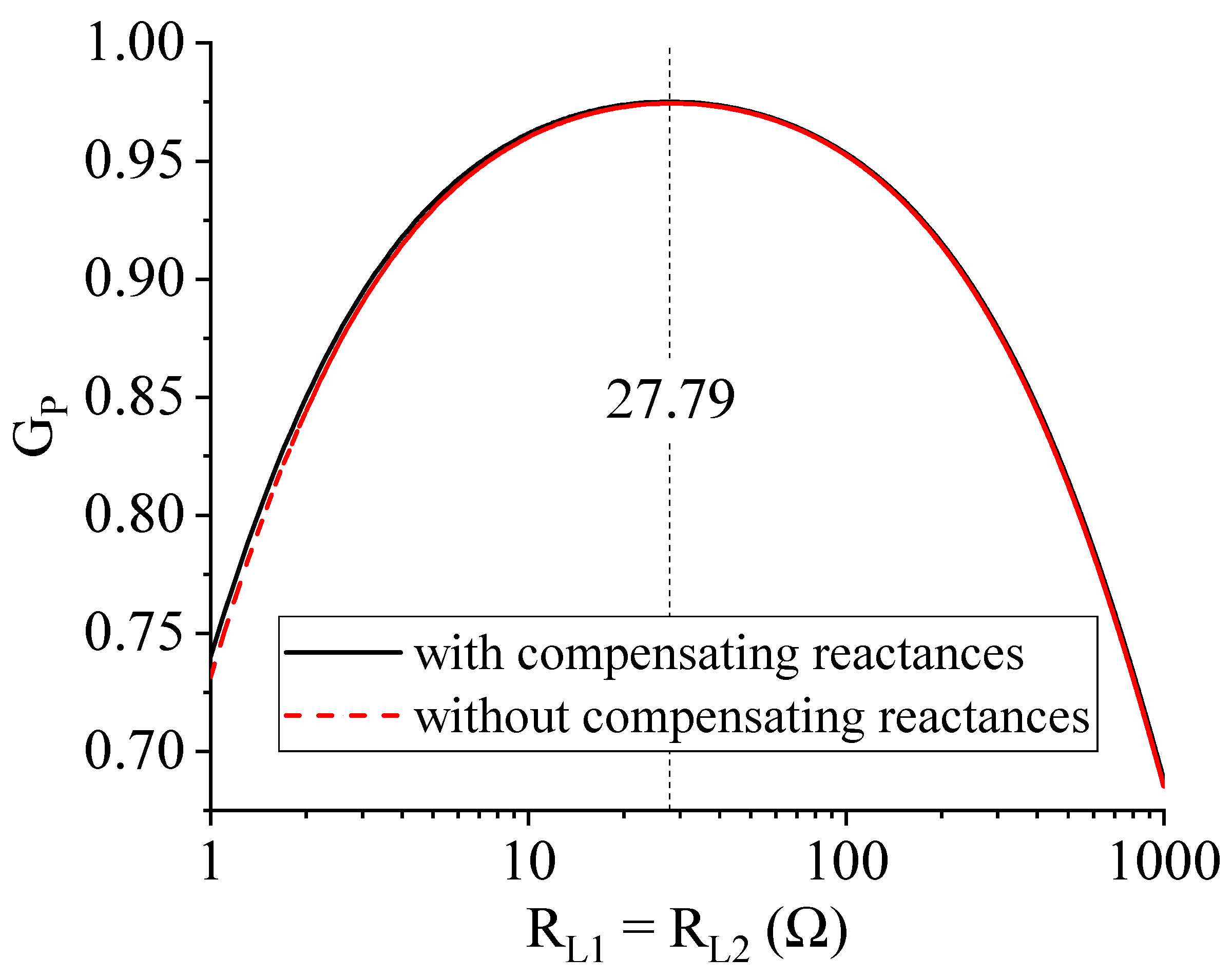
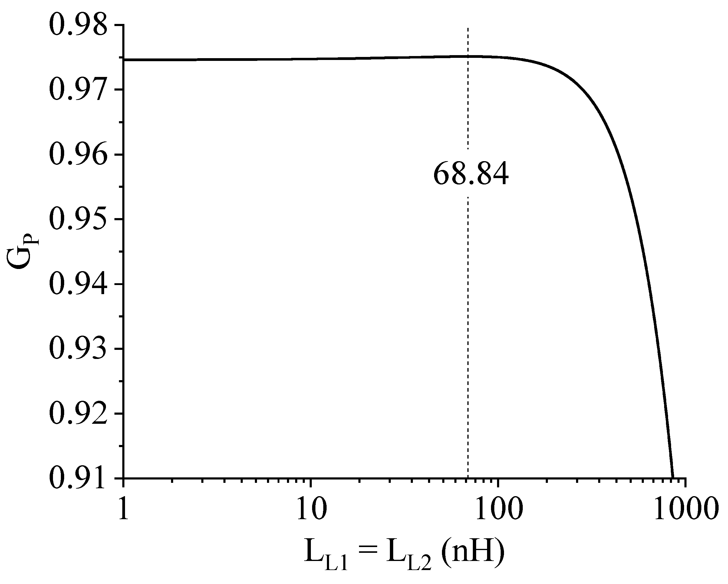
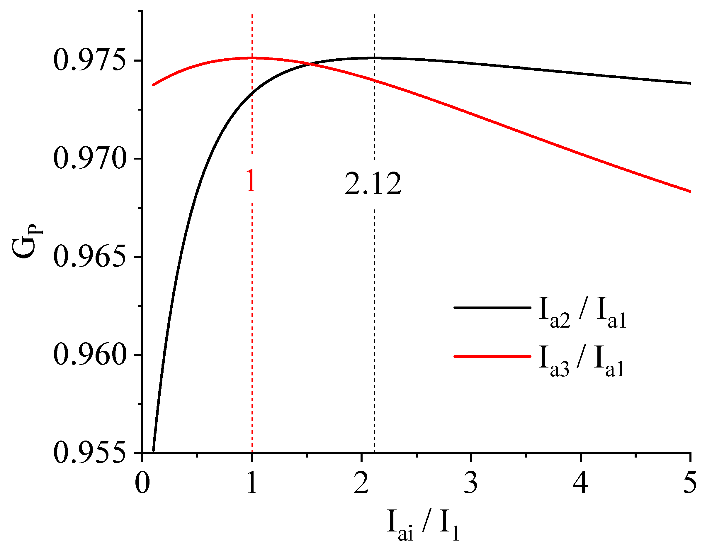
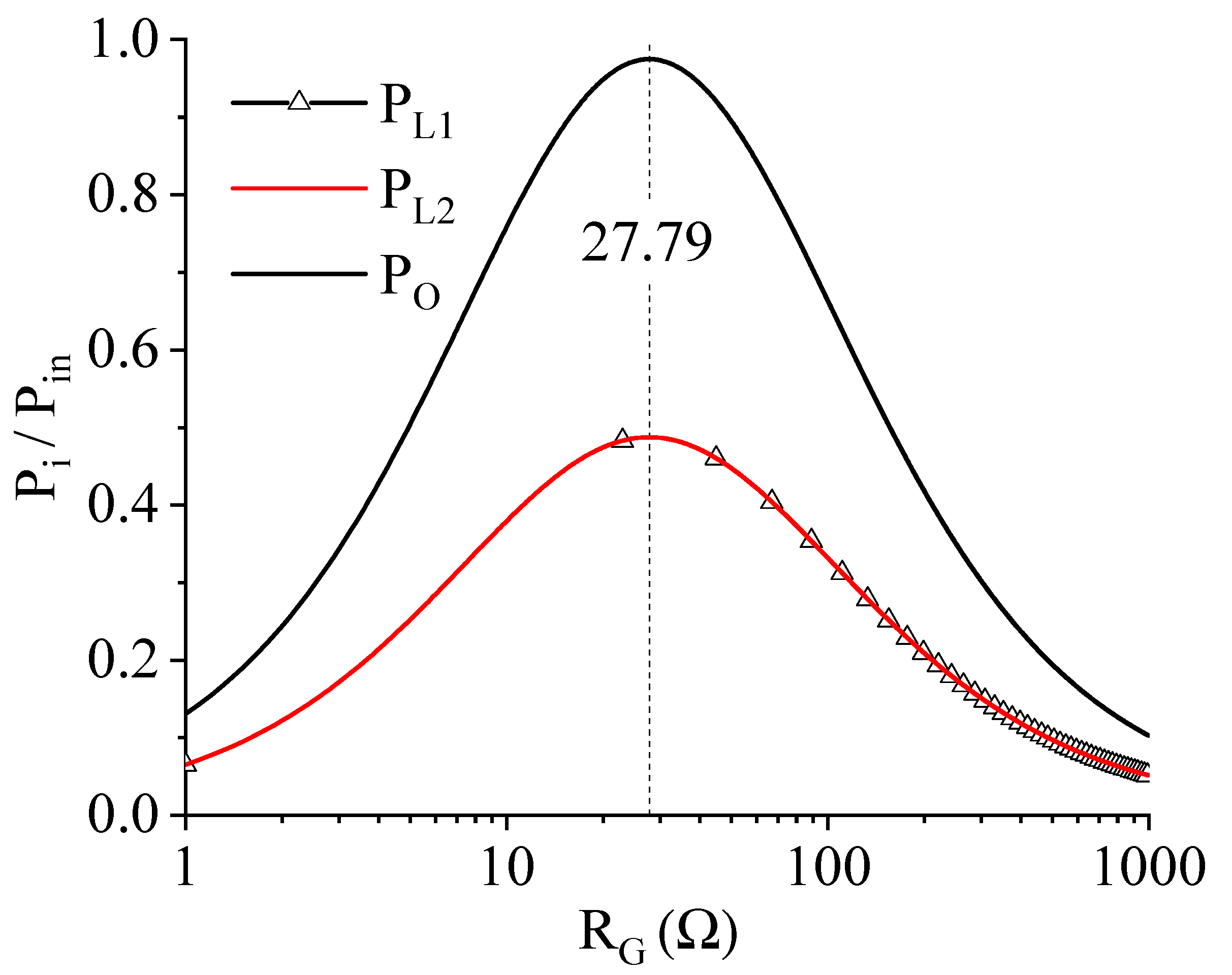
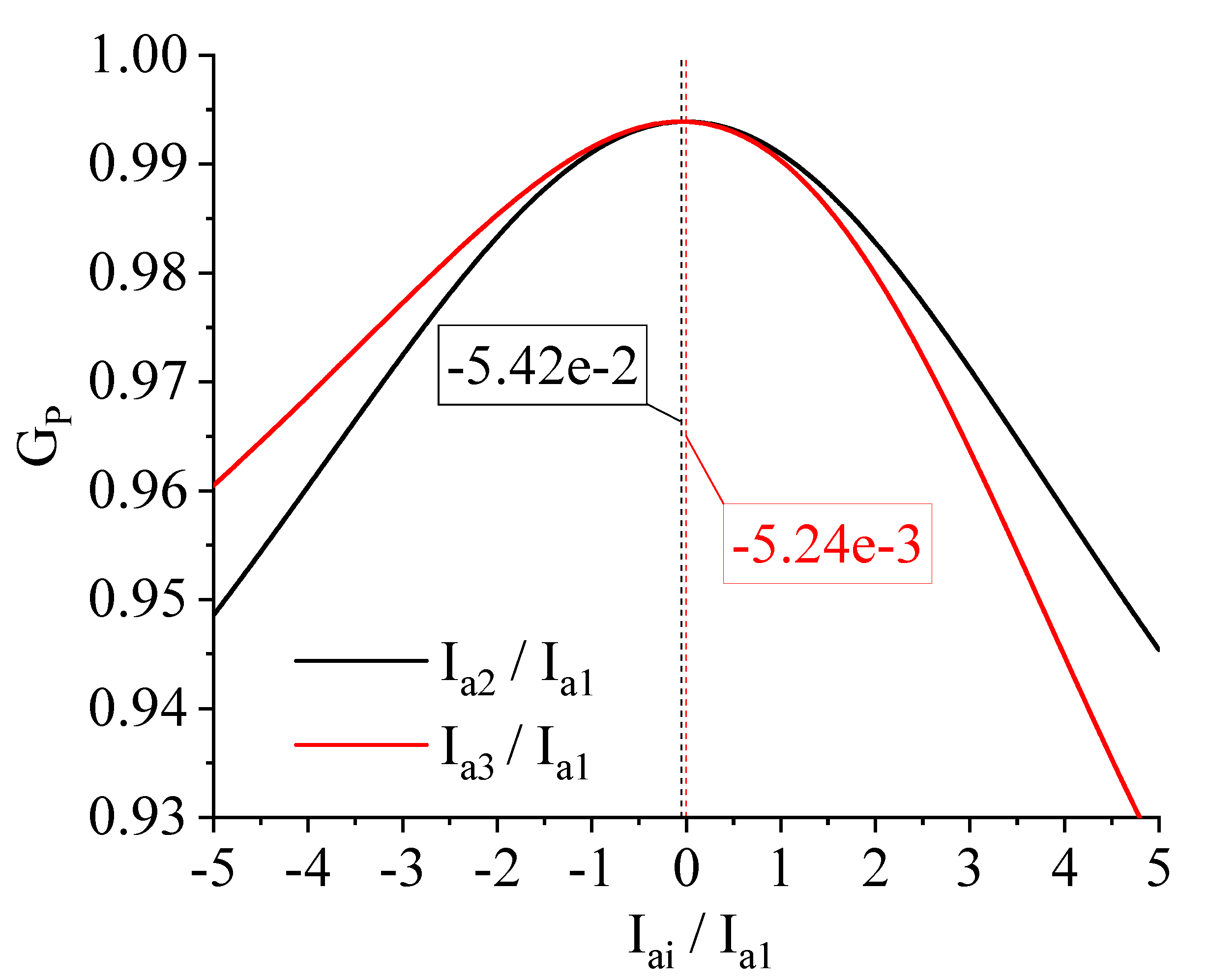
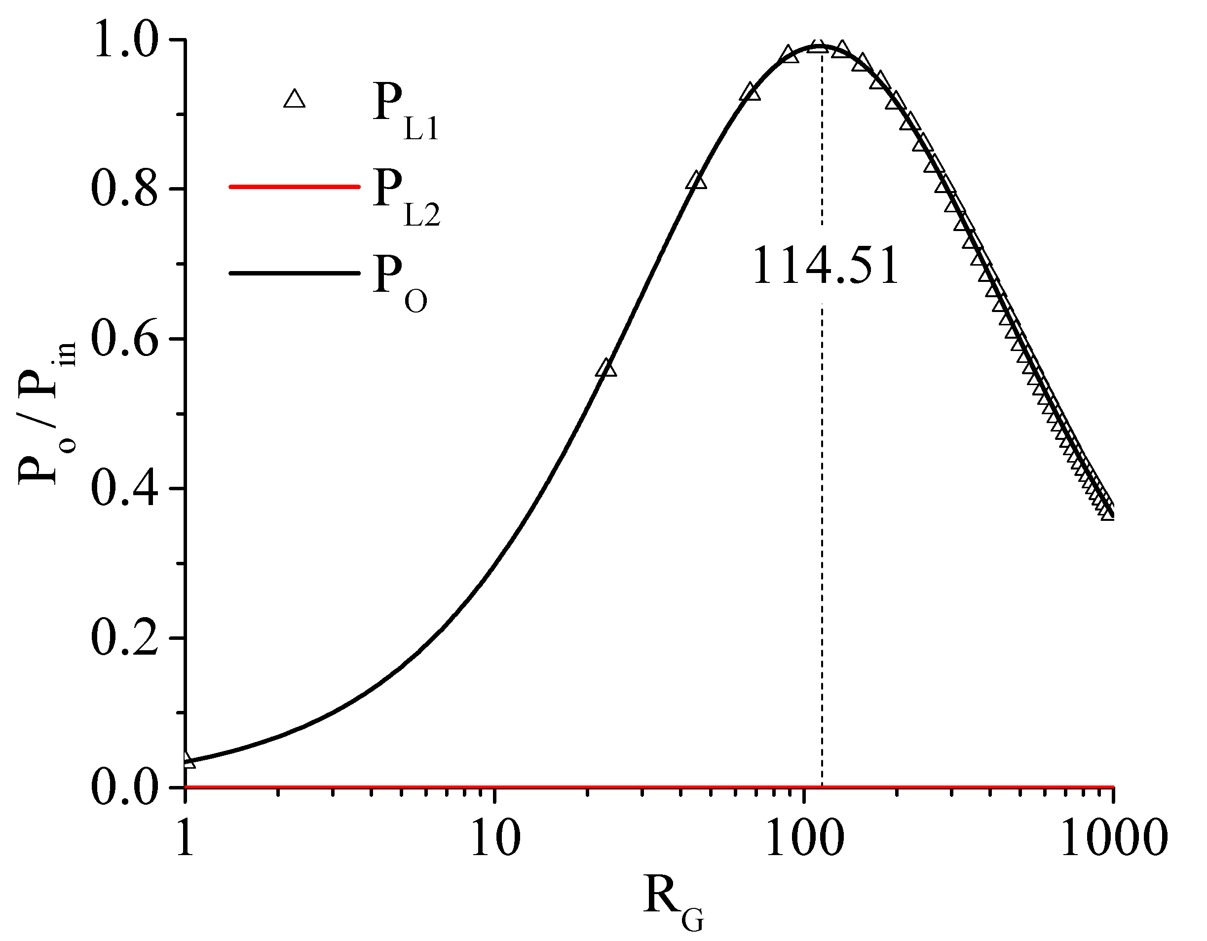
Numerical Results
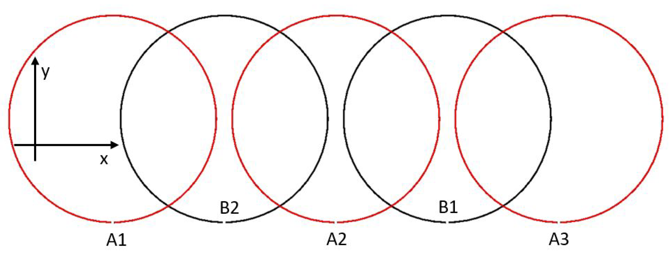
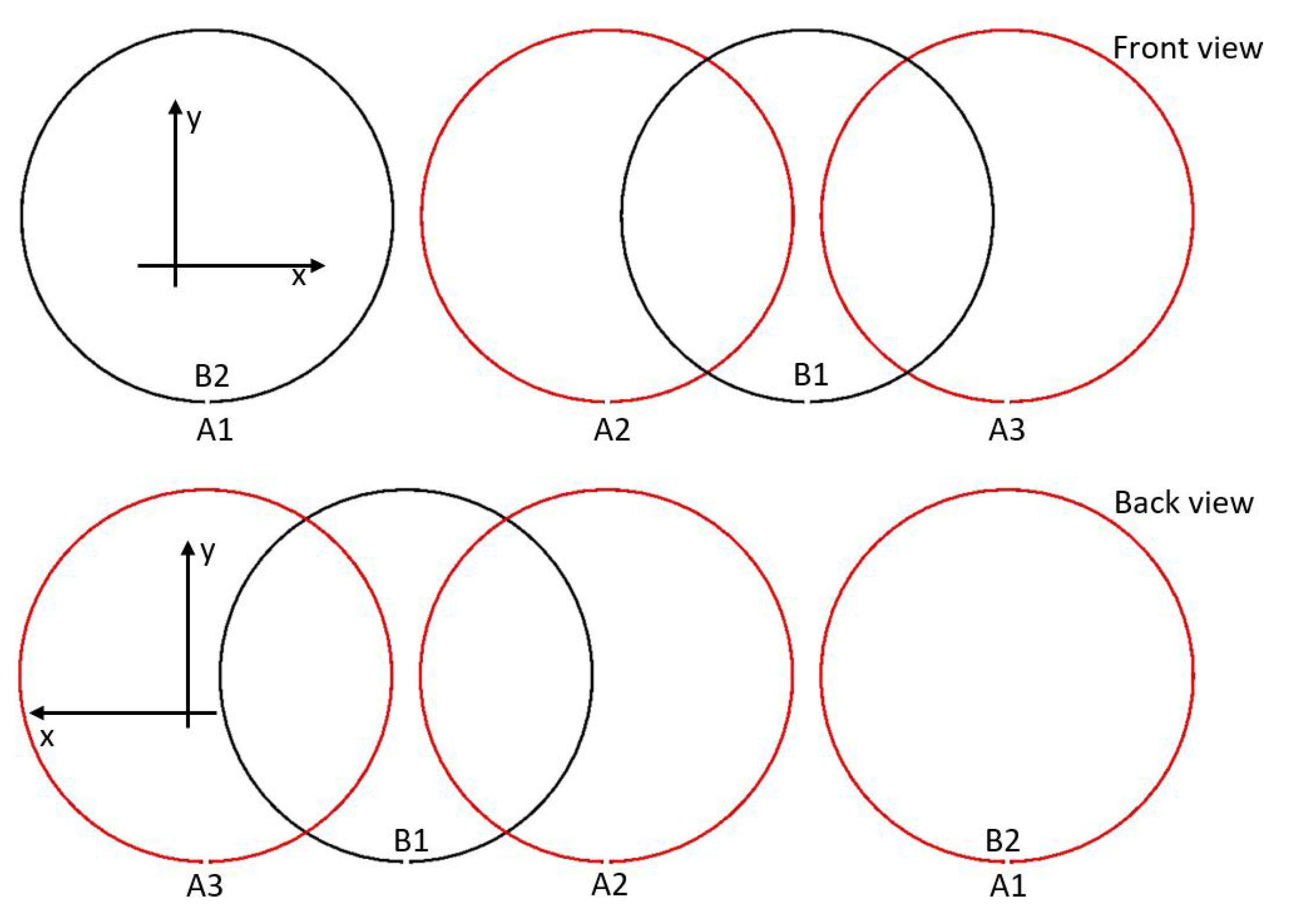
- Case 1,,,,;
- Case 2,,,,.
- Case 1: , 1,
- Case 2: , .
6. Conclusions
Author Contributions
Funding
Institutional Review Board Statement
Informed Consent Statement
Data Availability Statement
Acknowledgments
Conflicts of Interest
Appendix A. Some Insights into the Generalized Eigenvalue Problem
References
- Karalis, A.; Joannopoulos, J.D.; Soljačić, M. Efficient wireless non-radiative mid-range energy transfer. Ann. Phys. 2008, 323, 34–48. [Google Scholar] [CrossRef]
- Monti, G.; Paolis, M.V.D.; Corchia, L.; Tarricone, L. Wireless Resonant Energy link for Pulse Generators Implanted in the Chest. IET Microwaves Antennas Propag. 2017, 11, 2201–2210. [Google Scholar] [CrossRef]
- Carvalho, N.B.; Georgiadis, A.; Costanzo, A.; Stevens, N.; Kracek, J.; Pessoa, L.; Roselli, L.; Dualibe, F.; Schreurs, D.; Mutlu, S.; et al. Europe and the future for WPT. IEEE Microw. Mag. 2017, 18, 56–87. [Google Scholar] [CrossRef]
- Rim, C.T.; Mi, C. Wireless Power Transfer for Electric Vehicles and Mobile Devices; Wiley-IEEE Press: Hoboken, NJ, USA, 2017. [Google Scholar]
- Inagaki, N. Theory of Image Impedance Matching for Inductively Coupled Power Transfer Systems. IEEE Trans. Microw. Theory Tech. 2014, 62, 901–908. [Google Scholar] [CrossRef]
- Monti, G.; Costanzo, A.; Mastri, F.; Mongiardo, M. Optimal design of a wireless power transfer link using parallel and series resonators. Wirel. Power Transf. 2016, 3, 105–116. [Google Scholar] [CrossRef]
- Monti, G.; Costanzo, A.; Mastri, F.; Mongiardo, M.; Tarricone, L. Rigorous design of matched wireless power transfer links based on inductive coupling. Radio Sci. 2016, 51, 858–867. [Google Scholar] [CrossRef]
- Zhang, W.; Wong, S.; Tse, C.K.; Chen, Q. Design for Efficiency Optimization and Voltage Controllability of Series–Series Compensated Inductive Power Transfer Systems. IEEE Trans. Power Electron. 2014, 29, 191–200. [Google Scholar] [CrossRef]
- Zhang, W.; Wong, S.; Tse, C.K.; Chen, Q. Analysis and Comparison of Secondary Series- and Parallel-Compensated Inductive Power Transfer Systems Operating for Optimal Efficiency and Load-Independent Voltage-Transfer Ratio. IEEE Trans. Power Electron. 2014, 29, 2979–2990. [Google Scholar] [CrossRef]
- Mastri, F.; Mongiardo, M.; Monti, G.; Dionigi, M.; Tarricone, L. Gain expressions for resonant inductive wireless power transfer links with one relay element. Wirel. Power Transf. 2018, 5, 27–41. [Google Scholar] [CrossRef]
- Lee, J.; Lee, K. Effects of Number of Relays on Achievable Efficiency of Magnetic Resonant Wireless Power Transfer. IEEE Trans. Power Electron. 2020, 35, 6697–6700. [Google Scholar] [CrossRef]
- Alberto, J.; Reggiani, U.; Sandrolini, L.; Albuquerque, H. Accurate calculation of the power transfer and efficiency in resonator arrays for inductive power transfer. PIER 2019, 83, 61–76. [Google Scholar] [CrossRef]
- Johari, R.; Krogmeier, J.; Love, D. Analysis and practical considerations in implementing multiple transmitters for wireless power transfer via coupled magnetic resonance. IEEE Trans. Ind. Electron. 2014, 61, 1774–1783. [Google Scholar] [CrossRef]
- Yoon, I.; Ling, H. Investigation of near-field wireless power transfer under multiple transmitters. IEEE Antenna Wirel. Propag. Lett. 2011, 10, 662–665. [Google Scholar] [CrossRef]
- Lang, H.D.; Ludwig, A.; Sarris, C.D. Convex Optimization of Wireless Power Transfer Systems With Multiple Transmitters. IEEE Trans. Antennas Propag. 2014, 62, 4623–4636. [Google Scholar] [CrossRef]
- Pacini, A.; Costanzo, A.; Aldhaher, S.; Mitcheson, P.D. Load- and Position-Independent Moving MHz WPT System Based on GaN-Distributed Current Sources. IEEE Trans. Microw. Theory Tech. 2017, 65, 5367–5376. [Google Scholar] [CrossRef]
- Monti, G.; Che, W.; Wang, Q.; Costanzo, A.; Dionigi, M.; Mastri, F.; Mongiardo, M.; Perfetti, R.; Tarricone, L.; Chang, Y. Wireless Power Transfer With Three-Ports Networks: Optimal Analytical Solutions. IEEE Trans. Circuits Syst. 2017, 64-I, 494–503. [Google Scholar] [CrossRef]
- Li, Y.; Song, K.; Li, Z.; Jiang, J.; Zhu, C. Optimal Efficiency Tracking Control Scheme Based on Power Stabilization for a Wireless Power Transfer System with Multiple Receivers. Energies 2018, 11, 1232. [Google Scholar] [CrossRef]
- Sejin, K.; Hwang, S.; Kim, S.; Lee, B. Investigation of Single-Input Multiple-Output Wireless Power Transfer Systems Based on Optimization of Receiver Loads for Maximum Efficiencies. J. Electromagn. Eng. Sci. 2018, 18, 145–153. [Google Scholar]
- Fu, M.; Zhang, T.; Ma, C.; Zhu, X. Efficiency and Optimal Loads Analysis for Multiple-Receiver Wireless Power Transfer Systems. IEEE Trans. Microw. Theory Tech. 2015, 63, 3463–3477. [Google Scholar] [CrossRef]
- Monti, G.; Dionigi, M.; Mongiardo, M.; Perfetti, R. Optimal Design of Wireless Energy Transfer to Multiple Receivers: Power Maximization. IEEE Trans. Microw. Theory Tech. 2017, 65, 260–269. [Google Scholar] [CrossRef]
- Fu, M.; Yin, H.; Ma, C. Megahertz Multiple-Receiver Wireless Power Transfer Systems With Power Flow Management and Maximum Efficiency Point Tracking. IEEE Trans. Microw. Theory Tech. 2017, 65, 644–654. [Google Scholar] [CrossRef]
- Duong, Q.T.; Okada, M. Maximum efficiency formulation for inductive power transfer with multiple receivers. IEICE Electron. Exp. 2016, 22, 20160915. [Google Scholar] [CrossRef]
- Duong, Q.; Okada, M. Maximum Efficiency Formulation for Multiple-Input Multiple-Output Inductive Power Transfer Systems. IEEE Trans. Microw. Theory Tech. 2018, 66, 3463–3477. [Google Scholar] [CrossRef]
- Monti, G.; Mongiardo, M.; Minnaert, B.; Costanzo, A.; Tarricone, L. Optimal Terminations for a Single-Input Multiple-Output Resonant Inductive WPT Link. Energies 2020, 13, 5157. [Google Scholar] [CrossRef]
- Yuan, Q.; Aoki, T. Practical applications of universal approach for calculating maximum transfer efficiency of MIMO-WPT system. Wirel. Power Transf. 2020, 7, 86–94. [Google Scholar] [CrossRef]
- Desoer, C.A. The maximum power transfer theorem for n-ports. IEEE Trans. Circuit Theory 1973, 20, 328–330. [Google Scholar] [CrossRef]


| L | C | Q | |||||
| ( ) | ( ) | ( ) | |||||
| 1.88 | 73.28 | 460 | 13.56 | ||||
| Coupling coefficients | |||||||
| Optimal loads | |||||||
| , | , | ||||||
| ( ) | ( ) | ( ) | ( ) | ( ) | ( ) | ( ) | |
| 0.975 | 27.79 | 27.794 | 68.84 | 68.84 | 149.21 | 65.043 | 149.21 |
| L | C | Q | |||||
| ( ) | ( ) | ( ) | |||||
| 1.88 | 73.28 | 460 | 13.56 | ||||
| Coupling coefficients | |||||||
| Optimal loads | |||||||
| , | , | ||||||
| ( ) | ( ) | ( ) | ( ) | ( ) | ( ) | ( ) | |
| 0.994 | 114.51 | 114.51 | 36.30 | 0.108 | 6.72 | 0.215 | 766.49 |
Publisher’s Note: MDPI stays neutral with regard to jurisdictional claims in published maps and institutional affiliations. |
© 2021 by the authors. Licensee MDPI, Basel, Switzerland. This article is an open access article distributed under the terms and conditions of the Creative Commons Attribution (CC BY) license (https://creativecommons.org/licenses/by/4.0/).
Share and Cite
Monti, G.; Mongiardo, M.; Minnaert, B.; Costanzo, A.; Tarricone, L. Multiple Input Multiple Output Resonant Inductive WPT Link: Optimal Terminations for Efficiency Maximization. Energies 2021, 14, 2194. https://doi.org/10.3390/en14082194
Monti G, Mongiardo M, Minnaert B, Costanzo A, Tarricone L. Multiple Input Multiple Output Resonant Inductive WPT Link: Optimal Terminations for Efficiency Maximization. Energies. 2021; 14(8):2194. https://doi.org/10.3390/en14082194
Chicago/Turabian StyleMonti, Giuseppina, Mauro Mongiardo, Ben Minnaert, Alessandra Costanzo, and Luciano Tarricone. 2021. "Multiple Input Multiple Output Resonant Inductive WPT Link: Optimal Terminations for Efficiency Maximization" Energies 14, no. 8: 2194. https://doi.org/10.3390/en14082194
APA StyleMonti, G., Mongiardo, M., Minnaert, B., Costanzo, A., & Tarricone, L. (2021). Multiple Input Multiple Output Resonant Inductive WPT Link: Optimal Terminations for Efficiency Maximization. Energies, 14(8), 2194. https://doi.org/10.3390/en14082194