Article

A Bimodal Multichannel Battery Pack Equalizer Based on a Quasi-Resonant Two-Transistor Forward Converter

1
School of Electronic and Information, Hangzhou Dianzi University, Hangzhou 310018, China
2
School of Automation, Zhejiang Institute of Mechanical and Electrical Engineering, Hangzhou 310053, China
*
Author to whom correspondence should be addressed.
Energies 2021, 14(4), 1112; https://doi.org/10.3390/en14041112
Submission received: 31 December 2020 / Revised: 7 February 2021 / Accepted: 14 February 2021 / Published: 19 February 2021

Abstract

:
In the application of a long series battery group, an inter-pack imbalance is inevitable. No intra-pack cell equalizer can prevent pack-level over-discharge. A bimodal, multichannel battery pack equalizer based on a quasi-resonant, two-transistor forward converter is proposed to solve this problem and achieve a tradeoff between balancing efficiency and speed. This equalizer has two modes: pack-to-pack-group and pack-to-any-pack (P2PG&AP) mode and direct-pack-to-pack (DP2P) mode. In P2PG&AP mode, this equalizer can realize the full-switching-cycle (FSC) equalization through three balancing channels, and transfer energy from any pack to both the whole group and any pack inside the group. In addition, it can effectively clamp the transformer-induced voltage using a secondary side two-transistor magnetic reset structure (STMR) and reduce the total turns of transformer coil from 70 to 50 turns via a secondary side boost converter (SBC). In DP2P mode, this equalizer can realize zero voltage gap (ZVG) equalization. A prototype was tested at different switching frequencies and LC values to validate the theoretical analysis and optimize the bimodal hybrid operation. Experiment results including higher than 89.66% efficiency and minute-level balancing time under different pack voltage distributions show that the proposed topology demonstrates excellent balancing performance.

1. Introduction

Nowadays, the application of clean energy is a trend. Lithium-ion batteries are being more and more widely used [1]. As the cell voltage of a lithium-ion battery is low, battery packs made of a certain number of battery cells in series are used. Although the consistency of lithium batteries is constantly improving, the imbalances caused by slight differences of batteries in capacity, internal resistance, self-discharge rate, etc., are still unavoidable during use [2,3]. At present, there are many studies on the balancing technology of battery cells [4,5,6,7,8,9,10,11,12,13,14,15,16,17].
However, electric vehicles [18], mobile robots [19], space rovers [20,21], smart energy storage devices [22], and other high-power applications always need large numbers of in-series cells. In order to reduce the complexity of the cell equalizer and improve the reliability, several modular battery packs are series connected to form a pack group. For example, the battery group of Tesla Model S is composed of 16 series packs, and each pack has 6 cell parallel modules in series [23]. Obviously, the intra-pack cell equalizer cannot purposefully eliminate the imbalance between the battery packs, especially the pack-level over-discharge. Pack-level over-discharge means that there is a certain number of over-discharged batteries in one battery pack at the same time, and the total discharge time of the single battery pack is insufficient, which will cause the entire battery pack group to stop working. The effective solution is to use a pack equalizer.
The balancing strategy of pack equalizer is similar to the cell equalizer, which can also be divided into passive and active methods.
The passive method realizes equalization by dissipating the energy of overcharged battery through parallel power resistor [24]. Obviously, the passive method comes at the cost of reducing the overall discharge time of battery pack group.
In contrast, the active method can transfer the energy of the battery instead of venting it. Many studies have focused on the active method applied to a cell equalizer. This method can be divided into five categories: single to group [4,5], group to single [6,7], adjacent type [8,9,10,11], direct type [12,13,14,15], and hybrid type [16,17]. The active method’s energy transfer device can be an inductor, a capacitor, a transformer, or their combination. The disadvantages of active cell equalizers are higher cost and larger volume. Additionally, because of localized high temperature and complex EMI environment, the battery module’s reliability decreases with a significant increase in the number of active cell equalizers used. However, if these structures are applied to pack equalizer, the reduction in the number of balancing objects changing from cells to packs and the significantly dropped ratio of equalizer’s cost to power level are both obvious advantages.
According to different operation conditions, battery pack equalizers can be divided into cooperative and independent types. The cooperative type needs to cooperate with the intra-pack cell equalizer to perform its function [25,26,27]. It requires that the cell equalizer must have a cell-to-pack or pack-to-cell balancing function. Shang et al. [25] designed a modular multiwinding transformer to integrate the pack and cell equalizer. This integrated equalizer can achieve the balance between two or more designated battery packs by cooperating with cell equalization simultaneously, but at the cost of the transformer volume and leakage inductance loss. Farzan et al. [26] proposed a forward cell equalizer fed by a buck pack equalizer. This buck pack equalizer provides a DC bus for the pack-to-cell forward equalizer, and each cell equalizer is connected to the bus. The multiwinding forward transformer inside every pack realizes magnetic reset by the way of a parallel capacitor. Zhong et al. [27] used several 400V to 12 V DC-DC converters incorporating intra-pack BMSs and a low-voltage (LV) bus supply to realize the hierarchical model predictive control pack equalization.
The independent pack equalizer can balance battery packs independently, which means it can adapt to any structure of the lower cell equalizer [28,29]. This facilitates structure simplification and integration of the cell equalizer on a chip. Park et al. [28] introduced and compared a switch capacitor-based pack-to-pack equalizer and a flyback multiwinding transformer-based pack-to-pack equalizer respectively, and eventually chose a switched capacitor pack equalizer to reduce volume, cost, and energy consumption. However, its balancing speed is limited by the packs’ voltage difference. Dong et al. [29] proposed a multi-layer adjacent equalizer which relies on an inductor as an energy transfer device. Its bottom layer can balance adjacent cells, and its upper layer is responsible for balancing adjacent multicells or packs.
In general, restricted by the performance and cost of the power switch, the existing independent equalizer structures were relatively simple, and the cooperative pack equalizers were more common. Nevertheless, with the rapid development of MODFET manufacturing technology and pack-level SOC estimation [30], the superiority of an independent active pack equalizer has emerged.
This paper proposes a new active independent pack equalizer and makes three original contributions.
1.
Full-switching-cycle (FSC) equalization, which was verified by simulation and experimental waveforms, was innovatively realized by a quasi-resonant, two-transistor forward converter. This structure can not only limit the forward transformer’s induced EMF without the forward transformer’s magnetic reset coil, but also obtain three balancing channels in each switching cycle.
2.
The bimodal hybrid control strategy was designed to achieve a tradeoff between balancing efficiency and speed, which can select the best operation mode according to the status of battery pack group.
3.
The experimental data of the prototype, which was in good agreement with theoretical and simulation analysis, confirmed the proposed pack equalizer’s ability to prevent pack-level over-discharge.

2. Proposed Pack Equalizer

Before starting the system analysis, the abbreviations and explanations of all the special nouns in the paper are listed in Table 1.

2.1. Pack Equalizer Configuration and Operation Principles

The proposed bimodal multichannel pack equalizer, which takes a high-voltage battery pack but not a low-voltage battery cell as an equalization object, consists of a switch array, a two-transistor forward converter, an LC quasi-resonator, and a side boost converter (SBC), as shown in Figure 1a. It can use other channels or switch to the other mode when one balancing channel fails. This is of great significance to improve the reliability of high-power, fast inter-pack equalization.
The switch array can minimize the number of transformers and their windings in the pack equalizer topology. Compared with multi winding transformer and multi transformer structure, it has great advantages in cost reduction and the low weight of high-power pack equalizer. However, the cost is that the two power switches at the top and bottom of array need to be able to bear the voltage of entire pack group [4].
The two-transistor forward converter, composed of the forward transformer TP and STMR, is mainly used in pack-to-pack-group and pack-to-any-pack (P2PG&AP) mode. When the primary circuit turns on, TP transfers energy to the whole pack group through SBC. After the primary circuit turns off, the main part of the remanence energy in TP is transferred to the whole pack group through two magnetic reset diodes at the secondary side. This process realizes the voltage clamp of TP and FSC equalization simultaneously. The magnetic reset diodes are designed on the secondary side instead of the primary side. As a result, the primary coil-induced EMF of the off-state forward transformer can be further reduced by the effect of transformer turns ratio. Moreover, the other part of the remanence energy is stored in the capacitor CP1 to realize LC quasi-resonator to any pack (LC2AP) equalization. In DP2P mode, the primary circuit of TP is used as a part of the quasi-resonant loop to achieve ZVG equalization.
When SBC is not added, the turn ratio of transformer needs to be at least 1/6 to smoothly output the balancing current. This is because the turn-on resistance of MOSFETs and the forward turn-on voltage drop of diodes in the primary circuit will reduce the actual voltage of TP’s primary coil. SBC can quickly extract part of the energy charged into TP when the forward switch is on, and transfer it to the boost inductor LP2. The sum of the induced EMF of the secondary coil and LP2 can effectively raise the output voltage. When the turn ratio of the transformer is 1/4, it can also turn on D17 and D18 to output the balanced current. This greatly reduces the total turn ratio of TP and makes the transformer design miniaturized. At the same time, D17 and D18 clamp the voltage on Q14 to the total voltage of the entire battery pack group.
The LC series quasi-resonator has two functions. In P2PG&AP mode, CP1 can absorb the peak voltage of the transformer at the moment when the forward circuit turns off, and transmit this part of energy to any battery pack through the switch array in reverse; this auxiliary equalization function means that the equalizer can not only equalize from a single battery pack to the whole pack group, but also selectively equalize to any pack in group simultaneously in each switching cycle. Additionally, the equalization speed is improved innovatively, which is not available in the conventional single to group mode. In DP2P mode, CP1 and CP2 act as the core energy transfer device together with LP1. Q13 is used to select different capacitance values for quasi-resonator. A large CP1 value in P2PG&AP mode limits the switching frequency rise for keeping Q11 in a nearly zero-current switching state. This is detrimental to equalizer’s efficiency performance at high-power operation.
The proposed pack equalizer can cooperate with passive and chip intra-pack cell equalizers with the ability to prevent pack-level over-discharge. In the application of a long series battery group, this combination is simpler, lower cost, and smaller volume than the two-stage equalizers in [25,26,27]. The independent pack equalizer based on the switched capacitor in [28,29] can only achieve hour-level balancing speed, whereas the proposed pack equalizer can achieve minute level balancing speed.
Power Schottky diodes are used in the proposed pack equalizer. Their forward voltage drop is far lower than battery pack’s terminal voltage, which is a guarantee of high energy efficiency.
Compared with the cell equalizer, the switching devices of the pack equalizer need a higher withstand voltage. It is a fact that under the condition of the same withstand current value, MOSFETs with higher withstand voltage have lower switching speed, while the power diode with a higher withstand voltage has a higher forward voltage drop. These are the main factors affecting the equalizer efficiency. Moreover, a MOSFET with higher power and faster speed has a higher price. Thereby, although the switch array in the proposed topology has no theoretical limit on balancing objects’ number [4], in engineering, this number needs to achieve a compromise with energy efficiency and cost. In the following discussion of this paper, the balancing objects will be composed of four 20-series battery packs. In the application of a larger battery pack group, multiple proposed pack equalizers are used for inter-pack equalization, as shown in Figure 1b.

2.2. Operation Principles, Modeling, and Analysis of P2PG&AP Mode

In P2PG&AP mode, the proposed equalizer provides the first equalization path through TP during the on period of the forward switch. When the forward switch turns off, the equalizer generates the second equalization path through STMR to the whole group and the third equalization path from the LC quasi-resonator to a single pack. Differently from the conventional equalizer structure, which can only use part of the switching cycle to transfer energy, the proposed equalizer realizes the multichannel FSC equalization to effectively improve the equalization speed.
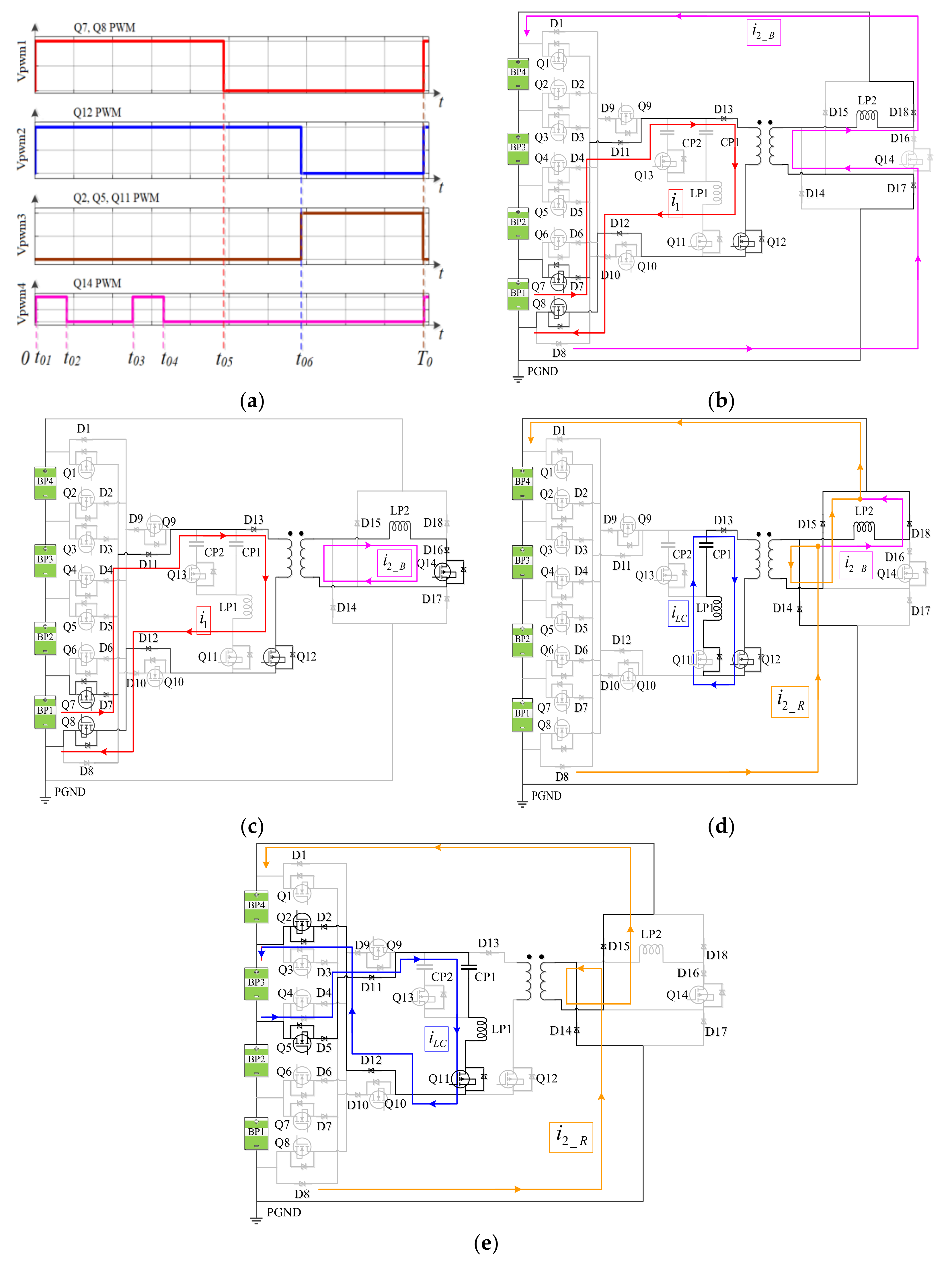
The switch pair Qi and Q(i + 1) in the switch array are driven by the same forward PWM wave with an adjustable duty cycle. Switch Q12 is driven by another synchronous PWM wave with higher duty cycle. Switch Q11 and another switch pair Qj and Q(j + 1) are driven by the PWM wave complementary to Q12′s PWM wave. The PWM signal of the SBC switch Q14 is obtained by superposition of two narrow pulse signals with identical duty cycles proportional to the forward PWM wave and the same frequency. Switches Q9, Q10, and Q13 are always off in this mode. The time sequence relationship of all PWM wave is shown in Figure 2a, and the period 0–t01 is the dead-time between forward switches and Q14. The relationship between the time points is as follows:
t 02 = t 01 + D B T 0 t 03 = t 01 + 0.5 D F T 0 t 04 = t 03 + D B T 0 t 05 = D F T 0 t 06 = ( 1 D L C ) T 0
where D F is the duty cycle of forward PWM wave, D B is the duty cycle of SBC PWM wave, and D L C is the duty cycle of LC quasi-resonator PWM wave.
Figure 2b–e shows the operation principle when BP1 releases energy to the whole pack group, and BP3 obtains the reverse charging from LC quasi-resonator. In the following analysis of P2PG&AP mode, this state will be used as the example.
State I (0–t01, Figure 2b): Q7, Q8, and Q12 are on simultaneously; the peak-induced voltage produced by TP’s secondary coil turns on D17 and D18 to output balancing energy to the whole group; as the voltage of the secondary side drops, the balancing current of the secondary side decreases.
State II (t01−t02, Figure 2c): Q14 is on, and the energy of TP is transferred to LP2.
State III (t02−t03, Figure 2b): Q14 turns off, and Q7, Q8, and Q12 stay on. The inductances of the TP secondary coil and boost inductor LP2 generate induced voltage to turn on D17 and D18 to output balancing energy to the whole group again.
State IV (t03–t04, Figure 2c) and state V (t04–t05, Figure 2b): State IV and state V respectively repeat the processes of state II and state III. Q14 remains off after t04 in each switching cycle.
State VI (t05–t06, Figure 2d): Q7 and Q8 turn off at t05, and Q12 remains in the on-state. Most of the remanence energy of TP charges to the whole pack group through D14 and D15. A small part of the remanence energy is stored in CP1 through Q12 and the body diode in Q11. The residual energy of LP2 continues to charge the whole pack group through D18 and D14 until the voltage of LP2 drops down.
State VII (t06–T0, Figure 2e): Q12 turns off, then Q11 turns on, the LC2AP equalization is activated. The energy of CP1 reversely charges to any battery pack selected by the controller through switch array. Additionally, the P2PG equalization through STMR continues until the remanence magnetic energy of the transformer is exhausted.
In the period of 0−t05, as shown in Figure 2b–c, the equalizer circuit meets the following expressions (ignoring C o s s of all MOSFETs and C j of all diodes):
E 1 = R m · ( i 1 i 2 _ B ) + L m · d ( i 1 i 2 _ B ) d t = V B P 1 L σ 1 · d i 1 d t i 1 · R e q 1 _ 1 i = 7 , 11 , 12 , 13 V F _ D i ( 0 < t t 05 ) E 2 = 4 E 1 = ( L σ 2 + L P 2 ) · d i 2 _ B d t + i 2 _ B · R e q 2 _ 1 + i = 17 , 18 V F _ D i + i = 1 4 V B P i ( 0 < t t 01 , t 02 < t t 03 , a n d t 04 < t t 05 ) E 2 = 4 E 1 = ( L σ 2 + L P 2 ) · d i 2 _ B d t + i 2 _ B · R e q 2 _ 2 + V F _ D 16 ( t 01 < t t 02 , t 03 < t t 04 )
where the explanations of parameters in Equation (2) are shown in Table 2. The positive direction and path of i 1 is indicated by the red arrows in Figure 2b,c. The positive direction and path of i 2 _ B is indicated by the purple arrows in Figure 2b,c,d.
By solving Equation (1) with i 1 ( 0 ) = i 2 _ B ( 0 ) = 0 and ignoring R m and all equivalent resistances, primary and secondary currents in the period of 0<t≤t01, t02<t≤t03, and t04<t≤t05 can be deduced as:
i 1 = i 1 ( t 0 x ) L m ( F + H ) + F G V B P 1 ( L m + G ) L m L σ 1 + ( L m + L σ 1 ) G ( t t 0 x ) i 2 _ B = i 2 _ B ( t 0 x ) H L σ 1 + L m ( F + H ) V B P 1 L m L m L σ 1 + ( L m + L σ 1 ) G ( t t 0 x )
Additionally, in the period of t01 < t ≤ t02, and t03 < t ≤ t04, they are:
i 1 = i 1 ( t 0 x ) + V B P 1 ( L m + G ) L m ( F + I ) F G L m L σ 1 + ( L m + L σ 1 ) G ( t t 0 x ) i 2 _ B = i 2 _ B ( t 0 x ) + V B P 1 L m I L σ 1 L m ( F + I ) L m L σ 1 + ( L m + L σ 1 ) G ( t t 0 x )
where F = i = 7 , 11 , 12 , 13 V F _ D i , G = ( L σ 2 + L P 2 ) / 4 , H = i = 17 , 18 V F _ D i / 4 + i = 1 4 V B P i / 4 , I = V F _ D 16 / 4 , and t 0 x is the initial moment of each switching state by turn.
According to Equations (3) and (4), when V B P 1 increases, i 1 and i 2 _ B increase; when L P 2 increases, i 1 and i 2 _ B decrease because L σ 1 is smaller than L m ; when F , H , or I increases, i 1 and i 2 _ B decrease.
In period of t05–T0, as shown in Figure 2d, e, the equalizer circuit meets:
E 1 = R m · ( i L C i 2 _ R ) + L m · d ( i L C i 2 _ R ) d t ( t 05 < t t 06 ) = L P 1 · d i L C d t + C P 1 1 · t 05 t 06 i L C d t + i L C · R e q 1 _ 2 + V F _ D 13 + V F _ Q 11 C P 1 1 · t 06 T 0 i L C d t + L P 1 · d i L C d t + i L C · R e q 1 _ 3 + i = 2 , 5 , 11 , 12 V F _ D + V B P 3 = 0 ( t 06 < t T 0 ) E 2 = 4 E 1 = L σ 2 · d i 2 _ R d t + i 2 _ R · R e q 2 _ 4 + i = 14 , 15 V F _ D i + i = 1 4 V B P i ( t 05 < t T 0 ) L P 2 · d i 2 _ B d t = i 2 _ B · R e q 2 _ 3 + i = 14 , 15 V F _ D i + i = 1 4 V B P i ( t 05 < t T 0 )
where the explanations of parameters in Equation (5) are also shown in Table 2. The positive direction and path of iLC is indicated by the blue arrows in Figure 2d,e. The positive direction and path of i2_R is indicated by the yellow arrows in Figure 2d and e.
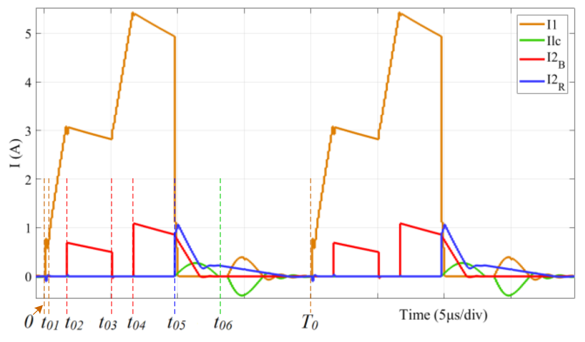
It can be found that the solution of Equation (5) is mathematically complex and not intuitive enough. MATLAB/Simulink simulation was done to verify the currents and the design parameters of the equalizer. The waveforms of currents are shown in Figure 3. Table 3 lists the relevant parameters of the simulation experiment.
In Figure 3, the trends of i 1 and i 2 _ B conform to Equations (3) and (4) during 0–t05. Furthermore, under suitable D F and D B , as shown in Table 3, the transformer is completely demagnetized when magnetic reset current drops to zero at the end of each cycle, and SBC works in discontinuous current mode. LC quasi-resonant current during t05–T0 is approximately sinusoidal.
In Figure 3, the trends of i 1 and i 2 _ B conform to Equations (3) and (4) during 0–t05. Furthermore, under suitable D F and D B as shown in Table 3, the transformer is completely demagnetized when magnetic reset current drops to zero at the end of each cycle, and SBC works in discontinuous current mode. LC quasi-resonant current during t05–T0 is approximately sinusoidal.
In the actual circuit design, we have to consider the fact that Q11 can not completely block the current of LC quasi-resonator during 0–t05 due to the output capacitance of Q11. This current can be described by the time domain expression of LC quasi-resonant current [12]:
i L C = 2 ( V B P 1 _ U V B P 1 _ D ) π R s sin ( 2 π f Q r t ) e R s 2 L P 1 t f Q r = 1 L P 1 C e q R s 2 4 L P 1 / 2 π C e q = ( C P 1 + C P 2 / / C o s s _ Q 13 ) / / C o s s _ Q 11     ( C P 1 + C o s s _ Q 13 ) C o s s _ Q 11 C P 1 + C o s s _ Q 13 + C o s s _ Q 11
where VBP1 is the average voltage value of BP1, VBPl_U and VBPl_D are upper and lower voltages of VBP1 fluctuation, Ceq is the equivalent capacitance of quasi-resonator, COSS_Q11 and COSS_Q13 are the output capacitance of Q11 and Q13, fQr is the frequency of quasi-resonator current in 0−t05.
It can be seen that a MOSFET with smaller COSS used as Q11 can effectively reduce the quasi-resonator current in 0−t05, but its on-state resistance will increase accordingly, which is detrimental to the energy efficiency of both P2PG&AP mode and DP2P mode.

2.3. Operation Principles, Modelling, and Analysis of DP2P Mode

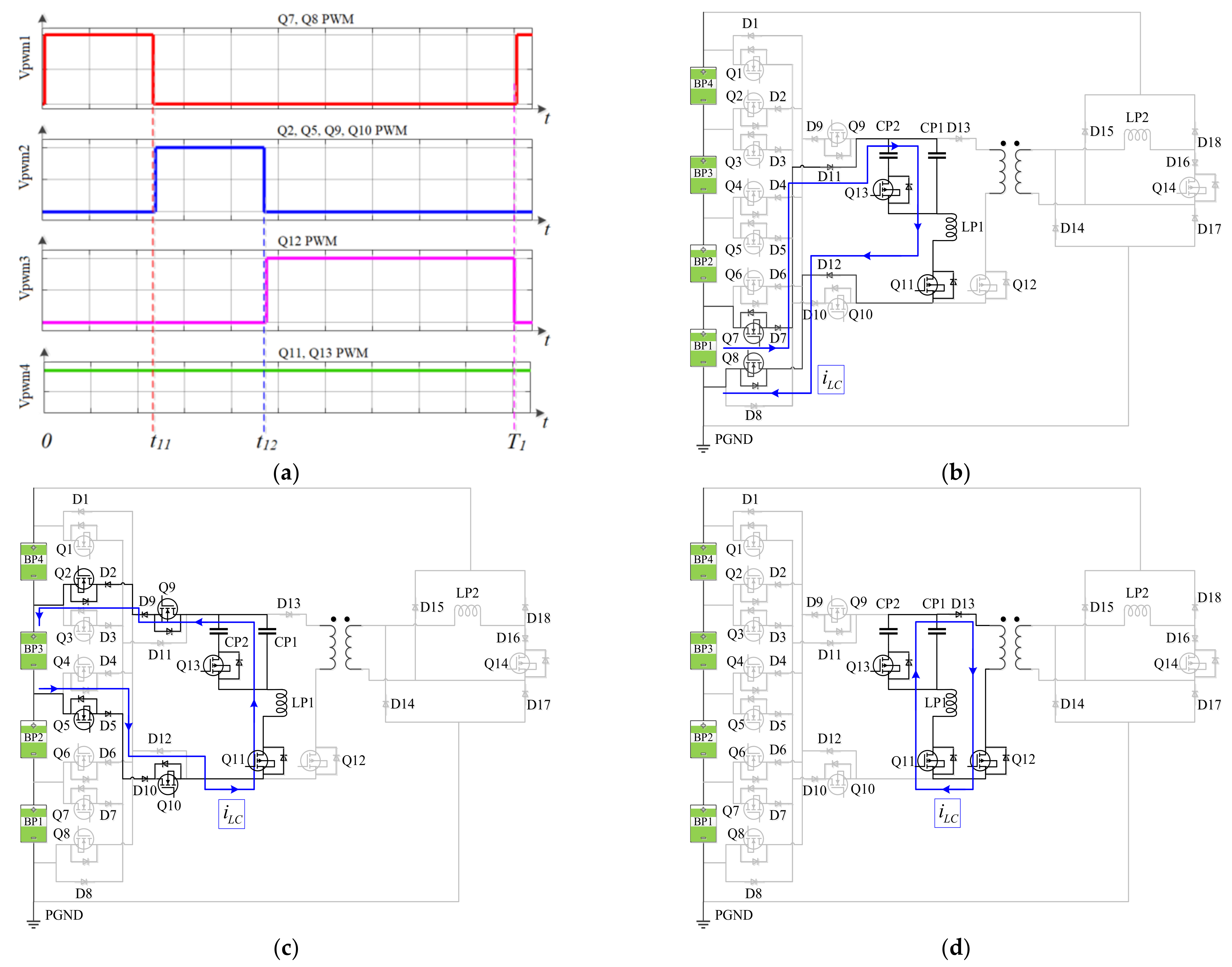
The DP2P mode is just a three state quasi-resonator [8] with direct balancing topology, which is suitable for situations where the voltage difference between battery packs is close to zero. In this mode, the switch pair Qi and Q(i + 1) connected to donor battery pack are first on. Additionally, the switch pair Qj and Q(j + 1) (j ≠ i) connected to acceptor battery pack turn on together with Q9 and Q10 after Qi and Q(i+1) turn off. The PWM wave of switch Q12 turns on the quasi-resonance to realize ZVG equalization after Qj, Q(j + 1), Q9 and Q10 turn off. In DP2P mode, Q11 and Q13 are always on, and Q14 is always off. Figure 4 shows the operation principle when BP1 is donor battery pack, and BP3 is acceptor battery pack. In the following analysis of DP2P mode, this state will be used as the example.
State I (0−t11, Figure 4b): After Q11 and Q13 turn on, Q7 and Q8 turn on simultaneously. BP1 charges the CP1, CP2, and LP1. The capacitor voltage increases from value V C d to V C u . At the same time, the discharge current of donor pack rises from 0, changes in the form of sine half wave. When the discharge current drops to 0, turn off the Q7 and Q8.
State II (t11−t12, Figure 4c): After Q7 and Q8 turn off, Q2, Q5, Q9, and Q10 turn on simultaneously, and the capacitor and inductor begin to release energy to BP3. The capacitor voltage decreases from value V C u to V Q r . The trend of charge current is similar to that of discharge current, but the direction is opposite. When the charge current drops to 0, turn off the Q2, Q5, Q9 and Q10.
State III (t12–T1, Figure 4d): After Q2, Q5, Q9 and Q10 turn off, Q12 turns on, and the capacitor and inductor form a quasi-resonant circuit. As the quasi-resonant current first increases and then returns to zero, the capacitor voltage decreases to value V C d . This process increases the gap between the voltage of BP1 and the capacitor voltage, speeds up the charging speed of BP1 to the capacitor and inductor in State I of the next cycle, thereby realizing the ZVG equalization between battery packs.
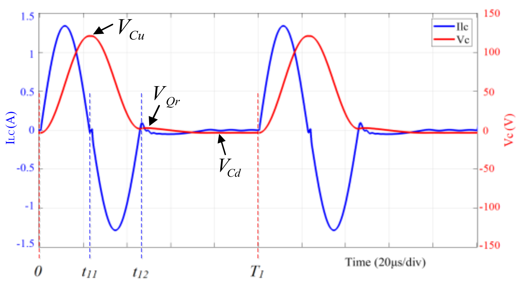
According to [8], the value of V C d , V C u , and V Q r as shown in Figure 5 are:
V C d = α ( α V B P 1 V B P 3 ) 1 α + α 2 V C u = V B P 1 + α 2 V B P 3 1 α + α 2 V Q r = ( 1 α ) V B P 3 1 α + α 2
where R s is the equivalent resistance of quasi-resonator, α and δ are defined as follows:
α = e π δ / 1 δ 2 1 δ 2 δ = R s 2 L P 1 / ( C P 1 + C P 2 )
The simulation waveforms in Figure 5 are obtained when V B P 1 = V B P 3 = 66 V with the same parameters in Table 3. This illustrates that the capacitor voltage can reduce to negative in the third stage of quasi-resonant process, and ZVG equalization can be achieved.

2.4. Equalizer Efficiency and Loss Analysis of P2PG&AP Mode

In this mode, the input power of the equalizer is the power provided by the donor battery pack:
P i n = p p r i m + p L C Q r + P T P _ p r i m = 1 T 0 0 t 05 V B P 1 i 1 d t
where the explanations of parameters in (9) are shown as Table 4.
In this mode, the output power of the equalizer is composed of three parts, including PSBC_out, PSTMR_out, and PLC_out, and their explanations are shown as in Table 4:
P o u t = P S B C _ o u t + P S T M R _ o u t + P L C _ o u t    = 1 T 0 ( 0 t 05 i = 1 4 V B P i i 2 _ B d t + t 05 T 0 i = 1 4 V B P i i 2 _ R d t + t 06 T 0 V B P 3 i 1 d t )
Therefore, the energy efficiency η P 2 P G & A P is as follows:
η P 2 P G & A P = P S B C _ o u t / P i n + P S T M R _ o u t / P i n + P L C _ o u t / P i n = η S B C + η S T M R + η L C
where the explanations of ηSBC, ηSTMR and ηLC are shown in Table 4.
Otherwise, the loss of equalizer mainly comes from the power loss of LC quasi-resonator, the circuit conduction loss, the switching loss, and the core loss of transformer.
According to Equation (6), the average power loss of LC quasi-resonator in 0−t05 can be calculated as follows:
p L C Q r = 1 T 0 0 t 5 v B P 1 i L C d t V B P 1 I L C I L C = 2 ( V B P 1 _ U V B P 1 _ D ) π 2 R s ( 1 R s 2 C e q 4 L P 1 ) ( 1 + e R s π 2 L P 1 C e q R s 2 4 )
where vBP1 is the real time value of donor pack voltage, ILC is the average value of LC quasi-resonant current.
It can be seen that pLCQr in 0−t05 is determined by pack voltage fluctuation and LC parameter. Moreover, the LC resonant frequency in 0−t05 is several times of the switching frequency in the design below.
The circuit conduction loss pcond is:
p c o n d = p c o n d 1 + p c o n d 2 p c o n d 1 = 1 T 0 · [ 0 t 05 i 1 2 · R e q 1 _ 1 d t + R e q 2 _ 1 · ( 0 t 01 i 2 _ B 2 d t + t 02 t 03 i 2 _ B 2 d t + t 04 t 05 i 2 _ B 2 d t ) + R e q 2 _ 2 · ( t 01 t 02 i 2 _ B 2 d t + t 03 t 04 i 2 _ B 2 d t ) ] ( 0 < t t 05 ) p c o n d 2 = 1 T 0 · [ t 05 t 06 [ i 1 · ( V F _ D 13 + V F _ Q 11 ) + i 1 2 · R e q 1 _ 2 ] d t ( t 05 < t T 0 ) + t 06 T 0 ( i 1 · i = 2 , 5 , 11 , 12 V F _ D i + i 1 2 · R e q 1 _ 3 ) d t + t 05 T 0 ( i 2 _ R · i = 14 , 15 V F _ D i + i 2 _ R 2 · R e q 2 _ 4 + i 2 _ B 2 · R e q 2 _ 3 ) d t ]
According to Equation (13), the conduction loss is mainly affected by primary current, secondary current, equivalent resistance, and forward voltage drop of diodes. Under the same balancing power level, the duty cycle of the equalizer is adjusted accordingly when the switching frequency changes. This means the peak and average value of primary current and the pack voltage fluctuation change little with switching frequency. Therefore, if the effect of other losses is not considered, the switching frequency has little effect on the above two kinds of losses in theory.
The switching loss pSW is:
p s w 1 = i = 7 , 8 , 14 p s w _ Q i + i = 7 , 11 , 12 , 16 , 17 , 18 p s w _ D i + p o p e n _ Q 12 + p o p e n _ D 13 p s w 2 = i = 2 , 5 , 11 p s w _ Q i + i = 2 , 5 , 11 , 12 , 14 , 15 p s w _ D i + p c l o s e _ Q 12 + p c l o s e _ D 13 p s w = p s w 1 + p s w 2
Additionally, the switching loss of MOSFET and diode are [31]:
p s w _ Q i = p o p e n _ Q i + p c l o s e _ Q i       = 0.5 f s w C o s s V o p e n 2 + 0.5 f s w V c l o s e I c l o s e t f a l l p s w _ D i = p o p e n _ D i + p c l o s e _ D i       = 0.5 f s w C j V o p e n 2 + 0.5 f s w V c l o s e I r r t r r
where psw_Qi and psw_Di are the switching losses of MOSFET and power diode, popen_Qi and pclose_Qi are the turn-on and turn-off losses of MOSFET, popen_Di and pclose_Di are the turn-on and turn-off losses of power diode. The explanations of other parameters in Equations (14) and (15) are shown in Table 4.
The core loss of transformer p c o r e is [32]:
p c o r e = c m c T f s w α ( L m N A e I m _ p p ) β I m _ p p = [ i 1 ( t 05 ) i 2 ( t 05 ) ] [ i 1 ( 0 ) i 2 ( 0 ) ] [ i 1 ( t 05 ) i 2 ( t 05 ) ]
where c m , c T , α , and β are the Steinmetz coefficients provided by manufacturer, N is the number of turns of the coil, A e is the effective cross sectional area of the magnetic core, I m _ p p is the peak-to-peak magnetizing current, and i 1 and i 2 are explained in Table 2.
When the switching frequency decreases, i 1 ( t 05 ) and i 2 ( t 05 ) increase. Since i 2 ( t 05 ) is proportional to i 1 ( t 05 ) and far less than it, [ i 1 ( t 05 ) i 2 ( t 05 ) ] increases. Additionally, β > α [32], so p c o r e will increase. However, increasing N or A e can reduce p c o r e , but they are constrained by the transformer conduction loss and volume.
Therefore, factors including the switching frequency, the type of the switching device, and the balancing power level, efficiency and the volume of the equalizer need to be fully considered in the design.

2.5. Equalizer Efficiency and Loss Analysis of DP2P Mode

In this mode, the average power of equalizer can be deduced according (7) and (8):
P i n = V B P 1 ( C P 1 + C P 2 ) ( V C u V C d )      = V B P 1 ( C P 1 + C P 2 ) ( 1 + α ) [ ( 1 α ) V B P 1 + α V B P 3 ] 1 α + α 2 P o u t = V B P 3 ( C P 1 + C P 2 ) ( V C u V Q r )      = V B P 1 ( C P 1 + C P 2 ) ( 1 + α ) [ V B P 1 ( 1 α ) V B P 3 ] 1 α + α 2
Therefore, the equalizer efficiency is as follows:
η D P 2 P = P o u t P i n = V B P 3 V B P 1 V B P 1 ( 1 α ) V B P 3 ( 1 α ) V B P 1 + α V B P 3
From (8) and (18), it can be found that η D P 2 P is affected by R s and L P 1 / ( C P 1 + C P 2 ) . Low R s and high L P 1 / ( C P 1 + C P 2 ) can effectively improve η D P 2 P .
On the other hand, the power loss of this mode mainly comes from the circuit conduction loss, the switching loss of MOSFET and power diode.
The circuit conduction loss pcond is:
p c o n d = 1 T 1 [ 0 t 11 ( i L C i = 7 , 11 , 12 V F _ D i + i L C 2 R e q 1 _ 4 ) d t + t 11 t 12 ( i L C i = 2 , 5 , 9 , 10 V F _ D i + i L C 2 R e q 1 _ 5 ) d t + t 12 T 1 ( i L C V F _ D 13 + i L C 2 R e q 1 _ 6 ) d t ]
Additionally, the switching loss p s w is:
p s w = i = 2 , 5 , 7 , 8 , 9 , 10 , 12 p s w _ Q i + i = 2 , 5 , 7 , 9 , 10 , 11 , 12 , 13 p s w _ D i
The calculation formula of p s w _ Q i and p s w _ D i is the same as (15).

3. The Bimodal Hybrid Control Strategy

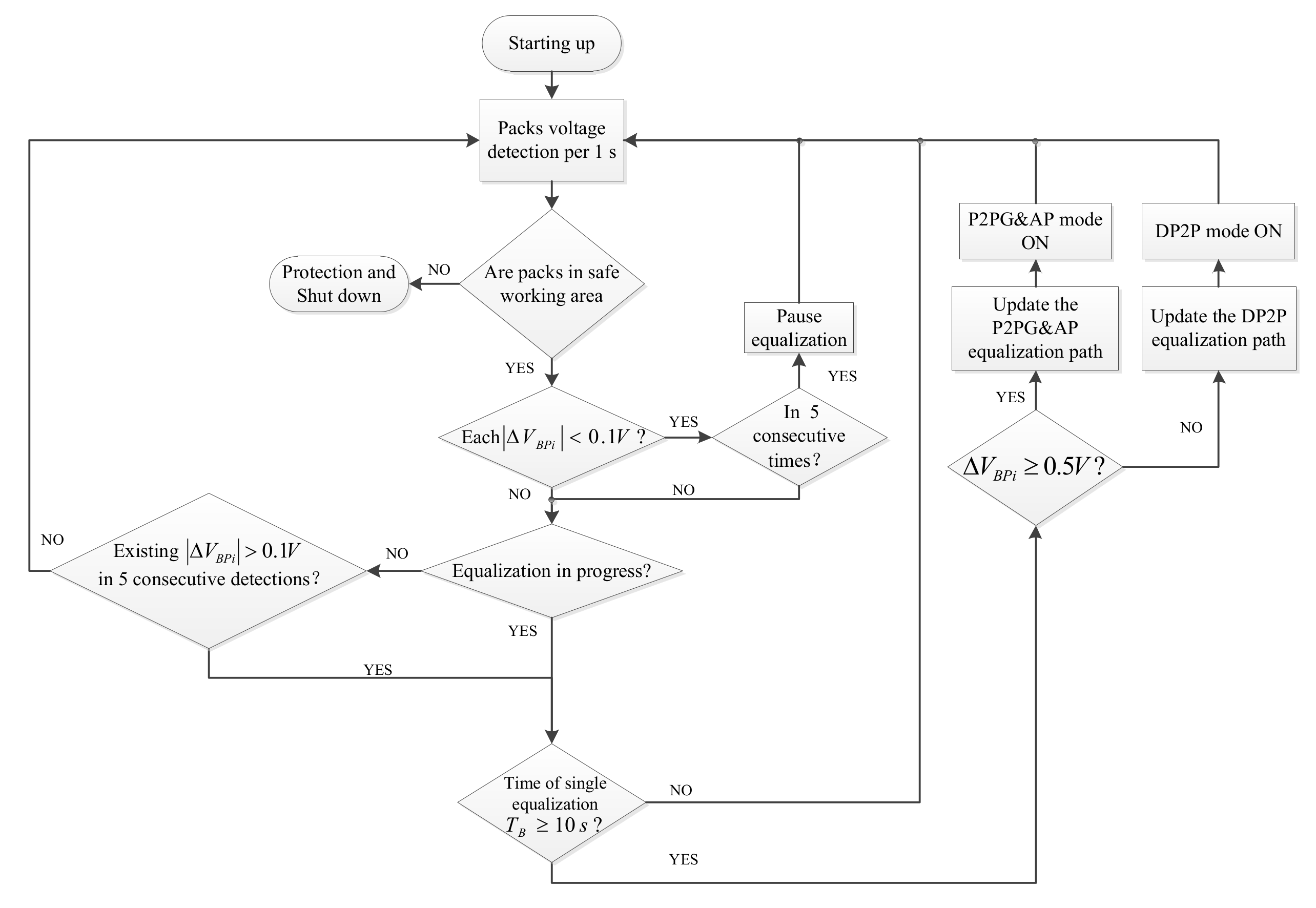
A bimodal hybrid strategy as shown in Figure 6 is used to control the proposed equalizer for four 20-series LiFePO4 battery packs. The voltage difference Δ V B P i between a single pack’s voltage and the pack group’s average voltage is used as the switching condition between P2PG&AP mode and DP2P mode. If there is a pack that Δ V B P i 0.5   V , the P2PG&AP mode is selected. Otherwise, DP2P mode is selected. This switching condition helps to prevent the repeated equalization caused by the faster voltage drop of the donor pack in P2PG&AP mode, and achieve a tradeoff between balancing efficiency and speed. Until each Δ V B P i 0.1   V in 5 consecutive voltage detection, the equalization is suspended. P2PG&AP mode selects the pack with the highest voltage as the donor pack for P2PG equalization, and the pack with the lowest voltage as the acceptor pack for LC2AP equalization after each voltage detection. DP2P mode selects the pack with the highest voltage as the donor pack, and the pack with the lowest voltage as the acceptor pack. A single equalization lasts for 10 s, and the equalization mode and path are updated after that.

4. Experiment Results

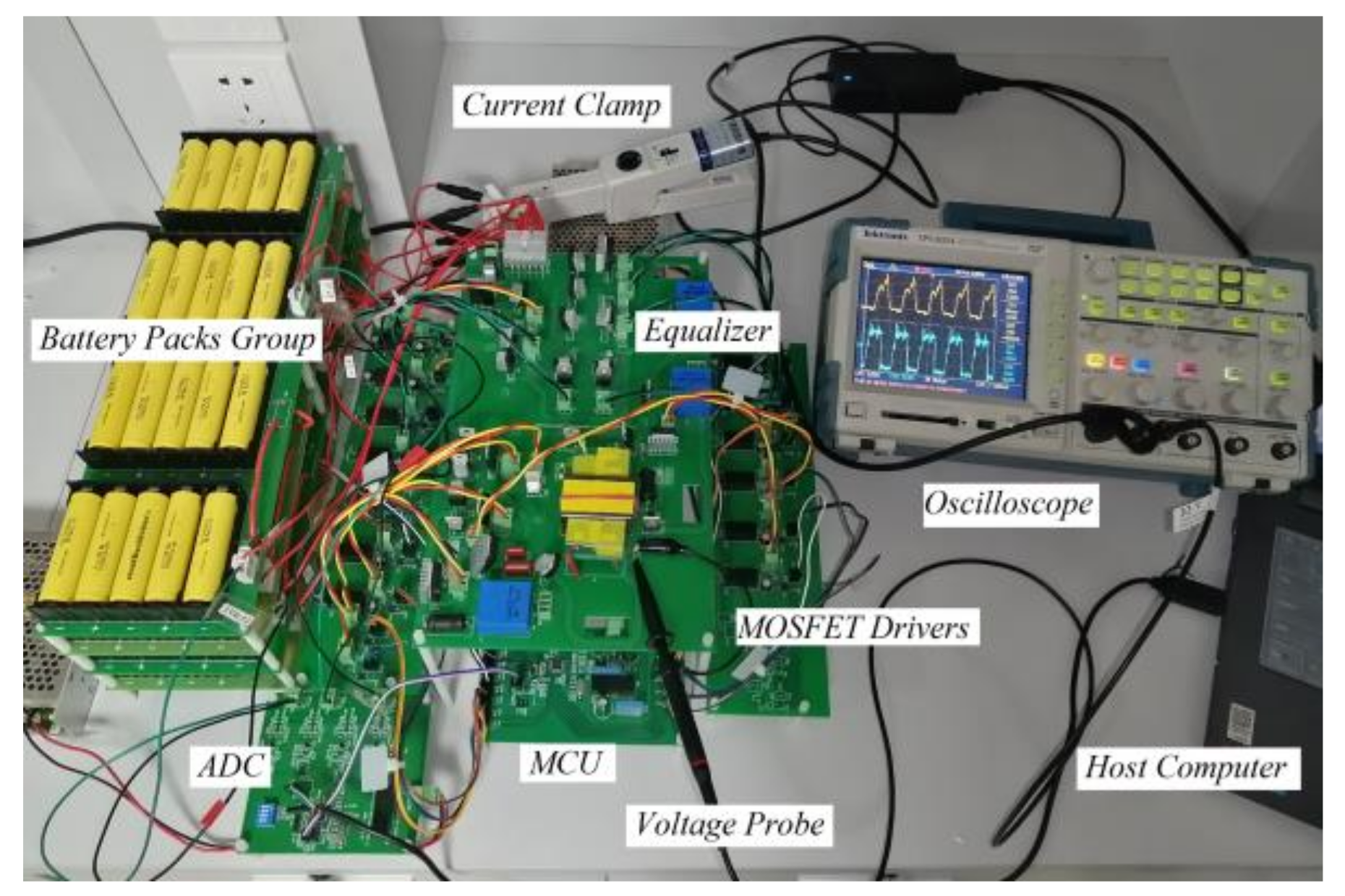
An experimental prototype was built for 4 series 66 V LiFePO4 battery packs with 1100 mAh capacity, as shown in Figure 7. The peak value of equalization current was limited to 6C to minimize the impact on battery life. In order to reduce the volume and the leakage inductance of the transformer as much as possible, a planar PCB-transformer was used, and the magnetic core was EEW43.2B (Mn-Zn ferrite) of DMEGC Magnetics Co., Ltd. (Zhejiang, China). In order to cooperate with the SBC to smoothly output balancing energy to the battery pack group during the forward conduction period of the P2PG&AP mode, the transformer turns ratio was 1/4. Table 5 lists the component parameters of prototype, and it can be seen from Table 5 that the sum of the selected diodes’ maximum forward voltage drop was very small compared with the battery pack terminal voltage. Table 6 lists the relevant parameters of the transformer. It can be seen from Table 6 that SBC can reduce at least 20 turns of secondary coil while keeping the primary inductance unchanged.
TPS2024 was used as the experimental measurement oscilloscope. The current clamps KEYSIGHT 1146B were used to measure the discharge current of donor pack, the STMR current was in P2PG&AP mode, and the LC quasi-resonant current was in DP2P mode. The current Hall sensors LA 25-NP/SP11 of LEM Electronics Co., Ltd. (Beijing, China) together with a 180 Ω measuring resistor were used to measure LC reverse charging current and the SBC output current in P2PG&AP mode.
Note: N 1 and N 2 are the primary and secondary winding turns; R w 1 and R w 2 are the primary and secondary winding resistances.

4.1. P2PG&AP Mode

In P2PG&AP mode experiments, V B P 2 is set to be the donor pack, V B P 3 is set to be the acceptor pack. In Figure 8a, the negative peak voltage of primary voltage waveform is 110 V, which indicates that can the forward transformer coil voltage is effectively clamped by the STMR together with LC series quasi-resonator. The waveform of discharge current of donor pack is similar to the simulation results in Figure 3. Additionally, at the moment the forward switch is on, its negative peak is caused by the reverse voltage of primary coil which is larger than donor pack voltage. In Figure 8b, it can be seen that in t05–t06, the transformer provides a small part of the remanence energy to the LC quasi-resonator, and the peak value of the approximate sinusoidal charging current is converted into 0.18 A according to Equation (21), its duration is about 2.8 μs. During t06–T0, the LC quasi-resonator charges the acceptor pack, and the peak value of the first negative half wave of the reverse charging current is converted to −0.23 A, its duration is about 4.2 μs.
I m e a s u r e = λ ( V H a l l / R m e a s u r e )
where λ = 40 is the conversion factor of LA 25-NP / SP11, and R m e a s u r e = 180   Ω is the value of measuring resistor.
This shows that the LC quasi-resonator still has a small part of the energy that is not completely released after the end of a switching cycle, because Q11 cannot completely prevent the LC quasi-resonator throughput energy in 0–t05. It can be seen from Figure 9b that the peak value of the ripple from sensor is 0.4 V, and the peak value of the ripple current calculated according to (21) is 0.09 A. Compared with the average discharge current of the donor pack 1.64 A in Figure 9a, it is acceptable. The reverse charging current will rise as the capacitor voltage rises to accelerate the release of LC energy, and fall back as the capacitor voltage drops.
In Figure 8c, the output current of SBC has 4 pulses in one switching cycle: the first low pulse is generated by the positive induced voltage of the secondary side at the moment the forward switch turns on; the second and third ones are SBC output current to pack group when Q14 shut down; the fourth pulse which is very close to the third one is the current produced by LP2′s residual energy after t05. The STMR current has one positive pulse and one negative pulse in one switching cycle: the positive one is just the two-transistor magnetic reset current after the forward switches turn off, its peak value is 3.92 A; the negative one is the short-term reverse recovery current of D14 and D15, its peak value is −1.92 A.
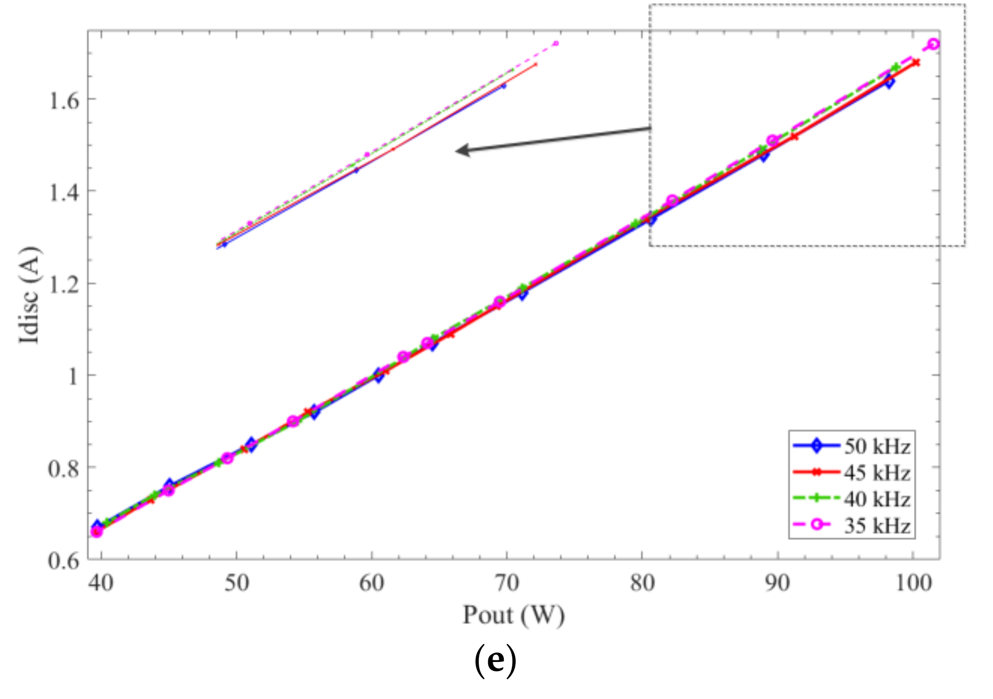
Figure 9 compares the measured total efficiency of equalizer and its three parts under different f s w . In Figure 9a, it can be observed that the peak value of η P 2 P G & A P is about 90.49% at 40 kHz and the corresponding output power is 54.5 W. The average η P 2 P G & A P reaches its maximum at 45 kHz, and drops with the decrease of f s w when f s w 45   k H z . This is because with the decrease of frequency, the core loss increases and a duty cycle larger than theory needs to be used in the actual circuit to obtain the designated balancing power. Figure 9e show that the average discharge current of donor pack increases with f s w decreases when balancing power is larger than 80 W.
Thereby, this fact leads to an extra increase of conduction loss. The average η P 2 P G & A P at 50 kHz is a little lower because of STMR performance and larger switching loss.
Figure 9b shows the trend of η S B C , the average η S B C decreases when f s w decreases because of the core loss, and the highest average and peak η S B C is both obtained at 50 kHz.
Figure 9c shows the trend of η S T M R , η S T M R increases when f s w deceases because the lower f s w can make the magnetic reset diodes have more time to turn off before the next cycle, and avoid the efficiency reduction caused by reverse recovery current.
Figure 9d shows the trend of η L C , η L C rises with f s w because its energy transmission time in each switching cycle is determined by LP1 and CP1 but not f s w . Additionally, with the increase of f s w , the sum of transmission time per unit time becomes larger.
To summarize, it can be observed that the trends of all parts of P2PG&AP mode efficiency are consistent with the analysis above, which prove the validity of Equations (12)–(16), and the total efficiency performance at 50 kHz is better when the output power is greater than 80 W. By considering that the balancing speed is given priority in P2PG&AP mode, the design of 50 kHz 98 W with 89.66% efficiency are selected to be used in bimodal hybrid operation.

4.2. DP2P Mode

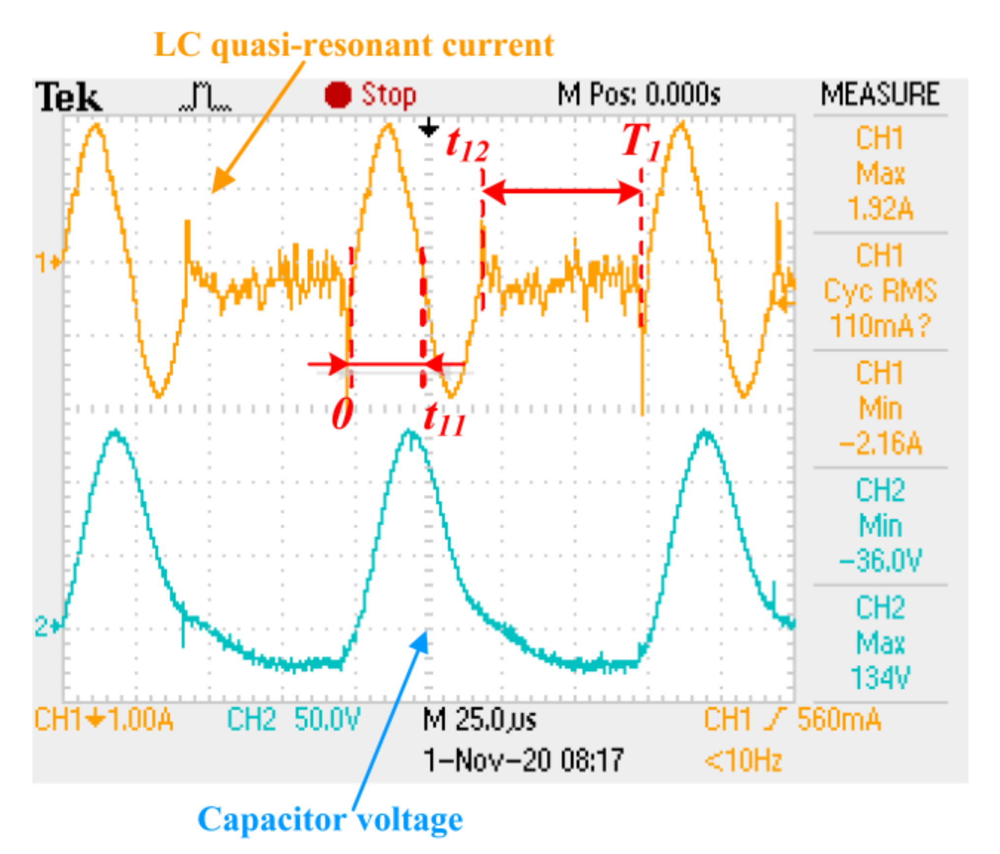
In DP2P mode experiments, V B P 2 is set to be the donor pack, V B P 3 is set to be the acceptor pack. In Figure 10, the peak value of the discharge current is 1.92 A and the duration is 22 μs. The negative peak value of the charge current is 1.84 A and the duration is 22 μs. The duration of the third resonant state is 56 μs. Since the output capacitance of Q14, the primary current waveform after Q12 turns on is affected by the secondary oscillating current, which is amplified and fed back to the primary side through the transformer. However, this does not affect the realization of equalization. As it can be found that the capacitor voltage decreases to negative value smoothly in the third resonant state.
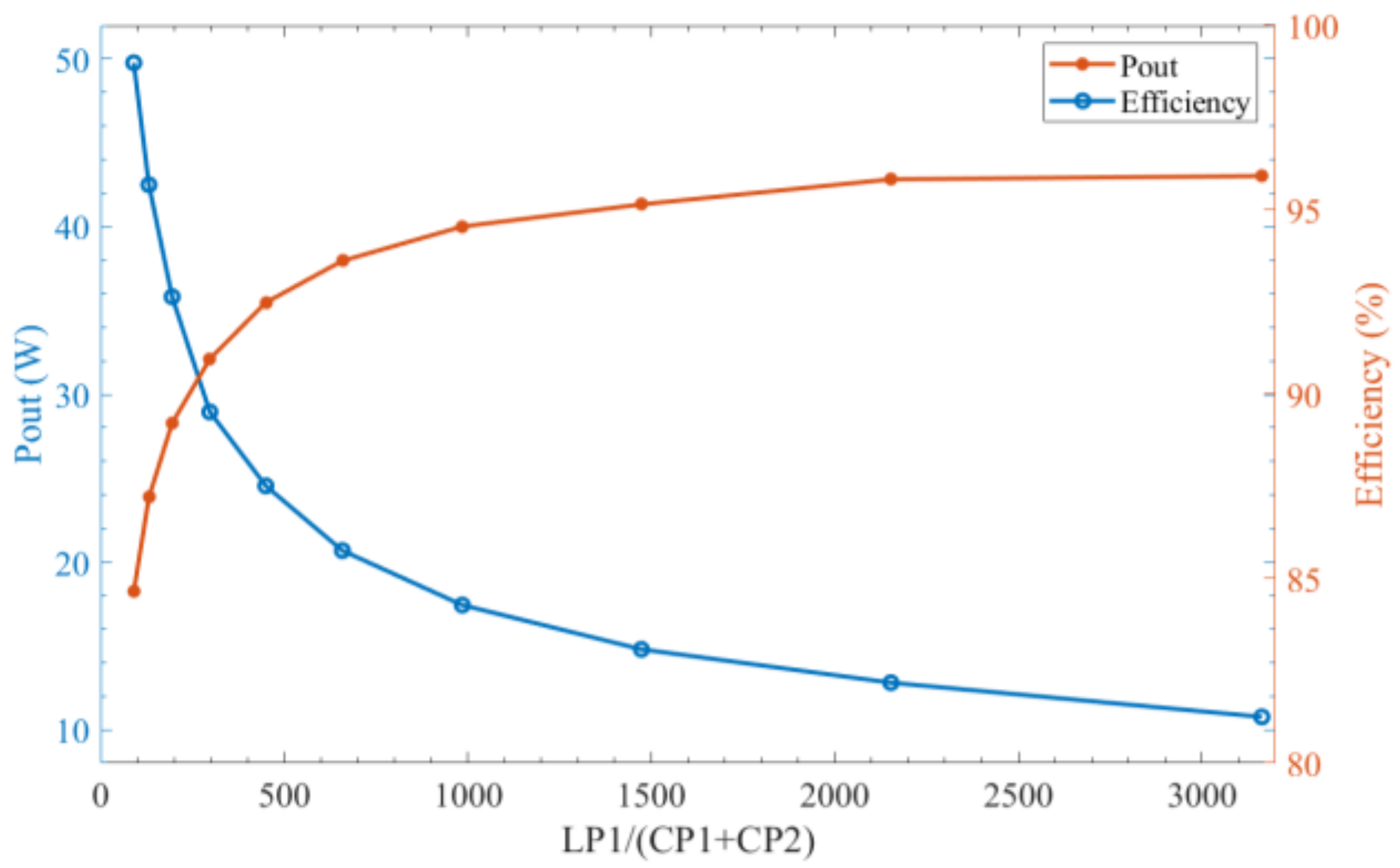
Figure 11 summarizes the variation trend of balancing efficiency and power with different ratio of inductor to capacitor value in 10 kHz DP2P mode, and verifies the analysis about Equation (18). Although higher efficiency can be obtained by increasing L P 1 / ( C P 1 + C P 2 ) , the output power of equalizer will decrease which means reduced balancing speed. When L P 1 / ( C P 1 + C P 2 ) rises above 2000, the growth in efficiency becomes very small. In order to balance the efficiency and speed of equalizer, a reasonable value of inductor and capacitor as shown in Table 5 is selected to be used in bimodal hybrid operation, and the corresponding efficiency achieves 95.8% with 13 W balancing power.

4.3. The Bimodal Hybrid Mode

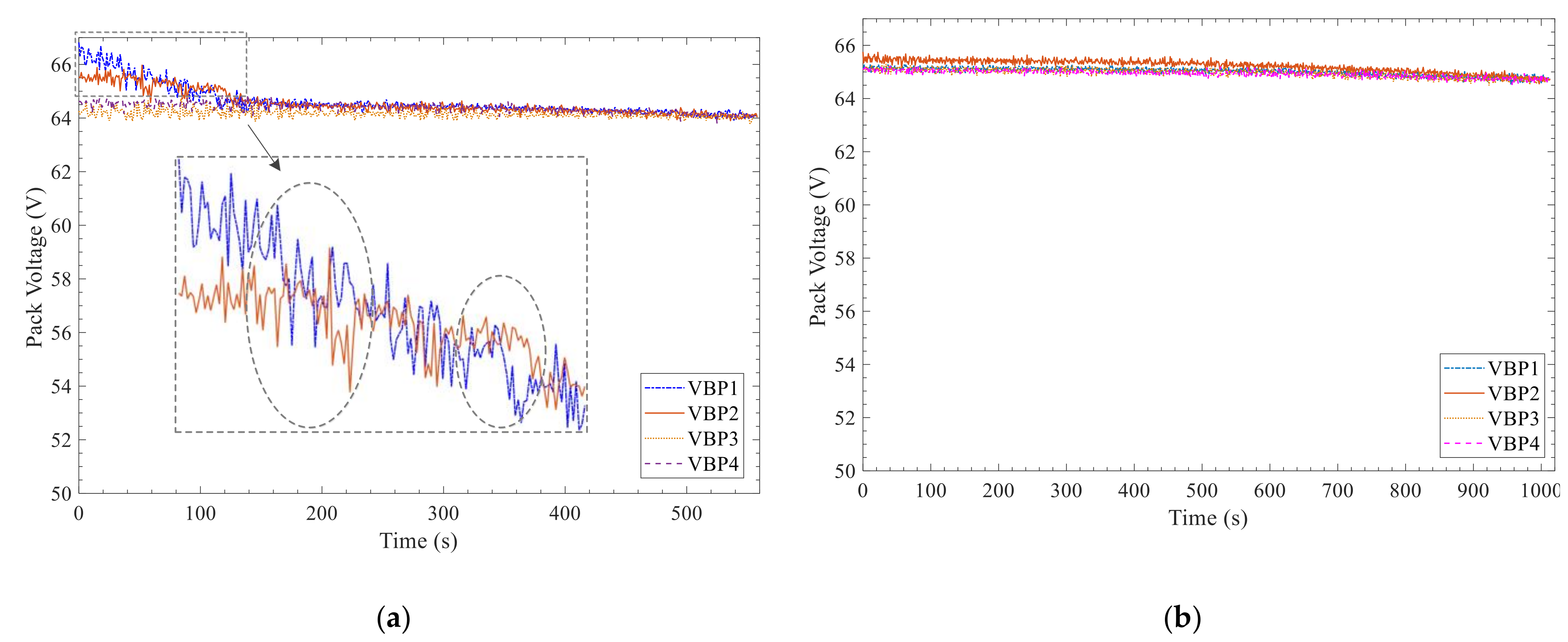
The voltage evolutions in the bimodal hybrid mode are presented in Figure 12 by testing the proposed equalizer with two initial equalization states during battery pack group discharged to the load at 0.6C, as shown in Table 7. The proposed pack equalizer operates in bimodal hybrid mode with the initial pack voltage distributions of Figure 12a, and in pure DP2P mode with the initial pack voltage distributions of Figure 12b.
It can be observed that all packs can be equalized simultaneously regardless of the pack voltage distributions, and this proves the robustness of the proposed equalizer to the initial imbalanced pack voltages. In Figure 12a, the equalizer worked in hybrid mode before 140 s, the donor pack voltage dropped faster in P2PG&AP mode, and then the equalizer switched to DP2P mode. The whole equalization process was completed in 558 s. In Figure 12b, the whole equalization process was completed in 1013 s. The proposed equalizer has much faster balancing speed than the conventional independent pack equalizers [28,29] with similar capacity battery objects but hour-level pack balancing time. Moreover, by comparison of Figure 12a, b, the balancing speed is found to be 45% faster in the hybrid mode than in pure DP2P mode.

5. Comparison with Conventional Pack Equalizers

Table 8 illustrates a comparison of existing battery pack equalizers in terms of power, efficiency, pack-level balancing speed and MOSFET withstand voltage. Additionally, Table 9 illustrates a comparison of these pack equalizers with their supporting cell equalizers in terms of component number, total size, and cost. It is assumed that the equalization objects include four 20-series battery packs. “AP2P” represents adjacent pack to pack topology. “PG2P” represents pack group to pack topology. “M” represents power MOSFETs, “D” represents power diodes, “W” represents the transformer windings used by equalizer, “T” represents transformers, “L” represents power inductors, and “C” represents energy storage capacitors. “SH” represents the pack equalizer sharing of the transformers with the cell equalizers in the pack. It can be seen that the proposed equalizer has clear superiority in terms of efficiency, relatively faster balancing speed, acceptable MOSFET withstand voltage and cost. In summary, the proposed equalizer is a more suitable solution for the applications of long series battery packs.

6. Conclusions

This paper proposed a battery pack equalizer based on quasi-resonant, two-transistor forward converter with two equalization modes which can be freely selected according to the state of battery packs, so as to improve the balancing speed and reliability of equalizer. An experimental prototype for four 20-series battery packs was built. The theoretical analysis of the equalizer efficiency was derived and verified by experiments at different frequencies. A bimodal hybrid control strategy was designed and tested in different initial pack voltage distributions to prevent pack-level over-discharge. The simulation and experimental results indicated that the proposed equalizer topology has the following superiorities:
(1)
The equalizer’s P2PG&AP mode can realize FSC equalization, as shown in Figure 3 and Figure 8. Additionally, ZVG equalization can be achieved in DP2P mode, as shown in Figure 5 and Figure 10.
(2)
An inter-pack equalization with minute level balancing time and more than 89.66% efficiency can be achieved through the bimodal hybrid control strategy, which can also effectively prevent the repeated equalization.
(3)
The equalizer is robust to different switching frequencies and different initial pack voltage distributions.
(4)
The proposed pack equalizer, which can cooperate with passive equalizer chips, provides a solution to simplify the structure of numerous cell equalizers in a long series battery group. This two-stage equalization scheme—which can be applied to electric vehicles, clean energy storage equipment and other fields—reduces the total number of power switches (including MOSFETs and power diodes) by at least 60%, and the total numbers of transformers and transformer coils by at least 75% and 97.5% respectively, as shown in Table 9.

Author Contributions

Conceptualization, Q.W. and M.G.; methodology, Q.W.; software, Q.W.; validation, Q.W., M.G., and H.L.; formal analysis, Q.W.; investigation, Q.W.; resources, Z.D.; data curation, Q.W.; writing—original draft preparation, Q.W.; writing—review and editing, Q.W.; visualization, Q.W.; supervision, M.G.; project administration, M.G.; funding acquisition, M.G. All authors have read and agreed to the published version of the manuscript.

Funding

This research was funded by the General Project of National Natural Science Foundation of China, grant number 61671194.

Institutional Review Board Statement

Not applicable.

Informed Consent Statement

Informed consent was obtained from all subjects involved in the study.

Data Availability Statement

The data presented in this study are available on request from the corresponding author. The data are not publicly available due to the data use agreement.

Conflicts of Interest

The authors declare no conflict of interest.

References

  1. Frost, D.F.; Howey, D.A. Completely Decentralized Active Balancing Battery Management System. IEEE Trans. Power Electron. 2018, 33, 729–738. [Google Scholar] [CrossRef]
  2. Wen, S. Cell Balancing Buys Extra Run Time and Battery Life. 2009. Available online: http://focus.ti.com/lit/an/slyt322/slyt322.pdf (accessed on 10 October 2019).
  3. Gallardo-Lozano, J.; Romero-Cadaval, E.; Isabel Milanes-Montero, M.; Guerrero-Martinez, M.A. Battery equalization active methods. J. Power Sources 2014, 246, 934–949. [Google Scholar] [CrossRef]
  4. Imtiaz, A.M.; Khan, F.H. “Time Shared Flyback Converter” Based Regenerative Cell Balancing Technique for Series Connected Li-Ion Battery Strings. IEEE Trans. Power Electron. 2013, 28, 5960–5975. [Google Scholar] [CrossRef]
  5. McCurlie, L.; Preindl, M.; Emadi, A. Fast Model Predictive Control for Redistributive Lithium-Ion Battery Balancing. IEEE Trans. Ind. Electron. 2017, 64, 1350–1357. [Google Scholar] [CrossRef]
  6. Shang, Y.; Zhao, S.; Fu, Y.; Han, B.; Hu, P.; Mi, C.C. A Lithium-Ion Battery Balancing Circuit Based on Synchronous Rectification. IEEE Trans. Power Electron. 2020, 35, 1637–1648. [Google Scholar] [CrossRef]
  7. Min, G.; Ha, J. Inner Supply Data Transmission in Quasi-Resonant Flyback Converters for Li-Ion Battery Applications Using Multiplexing Mode. IEEE Trans. Power Electron. 2019, 34, 64–73. [Google Scholar] [CrossRef]
  8. Shang, Y.; Cui, N.; Zhang, Q.; Zhang, C. A battery equalizer with zero-current switching and zero-voltage gap among cells based on three-resonant-state LC converters. In Proceedings of the 2017 IEEE Applied Power Electronics Conference and Exposition (APEC), Tampa, FL, USA, 26–30 March 2017; pp. 1647–1651. [Google Scholar]
  9. Ouyang, Q.; Chen, J.; Zheng, J.; Hong, Y. SOC Estimation-Based Quasi-Sliding Mode Control for Cell Balancing in Lithium-Ion Battery Packs. IEEE Trans. Ind. Electron. 2018, 65, 3427–3436. [Google Scholar] [CrossRef]
  10. Cao, X.; Zhong, Q.; Qiao, Y.; Deng, Z. Multilayer Modular Balancing Strategy for Individual Cells in a Battery Pack. IEEE Trans. Energy Convers. 2018, 33, 526–536. [Google Scholar] [CrossRef]
  11. Yuanmao, Y.; Cheng, K.W.E.; Yeung, Y.P.B. Zero-Current Switching Switched-Capacitor Zero-Voltage-Gap Automatic Equalization System for Series Battery String. IEEE Trans. Power Electron. 2012, 27, 3234–3242. [Google Scholar] [CrossRef]
  12. Shang, Y.; Zhang, Q.; Cui, N.; Duan, B.; Zhou, Z.; Zhang, C. Multicell-to-Multicell Equalizers Based on Matrix and Half-Bridge LC Converters for Series-Connected Battery Strings. IEEE J. Emerg. Sel. Top. Power Electron. 2020, 8, 1755–1766. [Google Scholar] [CrossRef]
  13. Chen, Y.; Liu, X.; Cui, Y.; Zou, J.; Yang, S. A MultiWinding Transformer Cell-to-Cell Active Equalization Method for Lithium-Ion Batteries With Reduced Number of Driving Circuits. IEEE Trans. Power Electron. 2016, 31, 4916–4929. [Google Scholar] [CrossRef]
  14. Ye, Y.; Cheng, K.W.E. Modeling and Analysis of Series–Parallel Switched-Capacitor Voltage Equalizer for Battery/Supercapacitor Strings. IEEE J. Emerg. Sel. Top. Power Electron. 2015, 3, 977–983. [Google Scholar] [CrossRef]
  15. Lee, K.; Chung, Y.; Sung, C.; Kang, B. Active Cell Balancing of Li-Ion Batteries Using $LC$ Series Resonant Circuit. IEEE Trans. Ind. Electron. 2015, 62, 5491–5501. [Google Scholar] [CrossRef]
  16. Park, S.; Park, K.; Kim, H.; Moon, G.; Youn, M. Single-Magnetic Cell-to-Cell Charge Equalization Converter with Reduced Number of Transformer Windings. IEEE Trans. Power Electron. 2012, 27, 2900–2911. [Google Scholar] [CrossRef]
  17. Mestrallet, F.; Kerachev, L.; Crebier, J.; Collet, A. Multiphase Interleaved Converter for Lithium Battery Active Balancing. IEEE Trans. Power Electron. 2014, 29, 2874–2881. [Google Scholar] [CrossRef]
  18. Hannan, M.A.; Hoque, M.M.; Peng, S.E.; Uddin, M.N. Lithium-Ion Battery Charge Equalization Algorithm for Electric Vehicle Applications. IEEE Trans. Ind. Appl. 2017, 53, 2541–2549. [Google Scholar] [CrossRef]
  19. Sauzé, C.; Neal, M. Artificial Endocrine Controller for Power Management in Robotic Systems. IEEE Trans. Neural Netw. Learn. Syst. 2013, 24, 1973–1985. [Google Scholar] [CrossRef]
  20. Govar, C.J.; Banner, J.A. Safety testing of lithium ion batteries for navy devices. IEEE Aerosp. Electron. Syst. Mag. 2003, 18, 17–20. [Google Scholar] [CrossRef]
  21. Sanguino, T.D.J.M.; Ramos, J.E.G. Smart Host Microcontroller for Optimal Battery Charging in a Solar-Powered Robotic Vehicle. IEEE/Asme Trans. Mechatron. 2013, 18, 1039–1049. [Google Scholar] [CrossRef]
  22. Yu, Y.; Saasaa, R.; Khan, A.A.; Eberle, W. A Series Resonant Energy Storage Cell Voltage Balancing Circuit. IEEE J. Emerg. Sel. Top. Power Electron. 2020, 8, 3151–3161. [Google Scholar] [CrossRef]
  23. Tear Down of 85 kWh Tesla Battery Pack Shows It Could Actually Only Be a 81 kWh Pack. Available online: https://electrek.co/2016/02/03/tesla-battery-tear&–85-kwh/Online (accessed on 12 January 2018).
  24. Gallardo-Lozano, J.; Romero-Cadaval, E.; Isabel Milanes-Montero, M.; Guerrero-Martinez, M.A. A novel active battery equalization control with on-line unhealthy cell detection and cell change decision. J. Power Sources 2015, 299, 356–370. [Google Scholar] [CrossRef]
  25. Shang, Y.; Xia, B.; Zhang, C.; Cui, N.; Yang, J.; Mi, C. A Modularization Method for Battery Equalizers Using Multiwinding Transformers. IEEE Trans. Veh. Technol. 2017, 66, 8710–8722. [Google Scholar] [CrossRef]
  26. Moghaddam, A.F.; Van den Bossche, A. Forward Converter Current Fed Equalizer for Lithium Based Batteries in Ultralight Electrical Vehicles. Electronics 2019, 8, 408. [Google Scholar] [CrossRef] [Green Version]
  27. Gong, Z.; van de Ven, B.A.; Gupta, K.M.; da Silva, C.; Amon, C.H.; Bergveld, H.J.; Donkers, M.T.; Trescases, O. Distributed Control of Active Cell Balancing and Low-Voltage Bus Regulation in Electric Vehicles Using Hierarchical Model-Predictive Control. IEEE Trans. Ind. Electron. 2020, 67, 10464–10473. [Google Scholar] [CrossRef]
  28. Park, H.; Kim, C.; Park, K.; Moon, G.; Lee, J. Design of a Charge Equalizer Based on Battery Modularization. IEEE Trans. Veh. Technol. 2009, 58, 3216–3223. [Google Scholar] [CrossRef]
  29. Dong, B.; Li, Y.; Han, Y. Parallel Architecture for Battery Charge Equalization. IEEE Trans. Power Electron. 2015, 30, 4906–4913. [Google Scholar] [CrossRef]
  30. Cai, H.; Hu, G. Distributed Control Scheme for Package-Level State-of-Charge Balancing of Grid-Connected Battery Energy Storage System. IEEE Trans. Ind. Inform. 2016, 12, 1919–1929. [Google Scholar] [CrossRef]
  31. Yuancheng, R.; Ming, X.; Jinghai, Z.; Lee, F.C. Analytical loss model of power MOSFET. IEEE Trans. Power Electron. 2006, 21, 310–319. [Google Scholar] [CrossRef]
  32. Roshen, W.A. A practical, accurate and very general core loss model for nonsinusoidal waveforms. In Proceedings of the Twentieth Annual IEEE Applied Power Electronics Conference and Exposition, APEC, Austin, TX, USA, 6–10 March 2005; Volume 1302, pp. 1308–1314. [Google Scholar]
Figure 1. The proposed pack equalizer. (a) The circuit diagram of the proposed pack equalizer. (b) The application in a larger battery pack group.
Energies 14 01112 g001
Figure 2. Operating principles of pack-to-pack-group and pack-to-any-pack (P2PG&AP) mode. (a) PWM wave sequence diagram of P2PG&AP mode. (b) State I,III and V. (c) State II,IV. (d) State VI. (e) State VII.
Energies 14 01112 g002
Figure 3. The simulation waveform of i 1 , i L C , i 2 _ B , i 2 _ R in P2PG&AP mode.
Energies 14 01112 g003
Figure 4. Operating principles of DP2P mode. (a) PWM wave sequence diagram of DP2P mode. (b) State I. (c) State II. (d) State III.
Energies 14 01112 g004
Figure 5. The waveform of capacitor voltage and quasi-resonant current.
Energies 14 01112 g005
Figure 6. The bimodal hybrid control strategy of proposed pack equalizer.
Energies 14 01112 g006
Figure 7. Photograph of the experimental prototype.
Energies 14 01112 g007
Figure 8. Experimental waveforms in 98 W, 50 kHz P2PG&AP mode when V B P 2 = 66.8   V , V B P 3 = 65.2   V , Δ V B P i = 65.7   V . (a) Primary current and primary winding voltage. (b) Q12 PWM wave and LC reverse charging current. (c) SBC output current and STMR current.
Energies 14 01112 g008
Figure 9. All parts of P2PG&AP mode efficiency and the average discharge current of donor pack at different f s w with the donor pack initial voltage of 66.8 V. (a) The total efficiency η P 2 P G & A P . (b) The SBC part of efficiency η S B C . (c) The STMR part of efficiency η S T M R . (d) The LC quasi-resonator part of efficiency η L C . (e) The average discharge current of donor pack.
Energies 14 01112 g009aEnergies 14 01112 g009b
Figure 10. Experimental waveforms of LC quasi-resonant current and capacitor voltage in 13 W, 10 kHz DP2P mode when V B P 2 = V B P 3 = 66.2 V.
Energies 14 01112 g010
Figure 11. The efficiency and P o u t of 10 kHz DP2P mode with different value of L P 1 / ( C P 1 + C P 2 ) .
Energies 14 01112 g011
Figure 12. Comparison of the pack voltage equalization result in bimodal hybrid mode and in pure DP2P mode. (a) Bimodal hybrid mode. (b) Pure DP2P mode.
Energies 14 01112 g012
Table 1. The abbreviations and explanations of all the special nouns.
AbbreviationsExplanations
P2PG&APpack-to-pack-group and pack-to- any-pack
DP2Pdirect-pack-to-pack
STMRsecondary side two-transistor magnetic reset structure
SBCsecondary side boost converter
FSCfull-switching-cycle
ZVGzero voltage gap
LC2APLC quasi-resonator to any pack
Table 2. Parameters and related explanations in the analysis of a pack equalizer.
ParametersExplanations
E 1 the EMF value of TP’s primary coil
E 2 the EMF value of TP’s secondary coil
R m the excitation impedance value of TP
i 1 the current value of primary side electrified circuit under different switching states
i 2 the output current value of secondary coil under different switching states
i 2 _ B the SBC current
i L C the quasi-resonator current
i 2 _ R the STMR output current
L m the excitation inductance of TP
V B P i the voltage value of the battery pack BPi
L σ 1 the leakage inductance of TP’s primary coil
L σ 2 the leakage inductance of TP’s secondary coil
R e q 1 _ 1 the total equivalent resistance of the primary side electrified circuit in Figure 2b,c
R e q 1 _ 2 the total equivalent resistance of the primary side circuit in Figure 2d
R e q 1 _ 3 the total equivalent resistance of the primary side circuit in Figure 2e
V F _ D the sum of the forward voltage drop of diodes on the energized circuit
L P 1 the inductance value of LC quasi-resonator
L P 2 the boost inductance value of the secondary side
C P 1 the capacitance value of LC quasi-resonator
C o s s The output capacitance of MOSFET
C j The junction capacitance of power diode
R s The equivalent resistance of quasi-resonator
R e q 2 _ 1 the total equivalent resistance of the secondary side electrified circuit in Figure 2b
R e q 2 _ 2 the total equivalent resistance of the secondary side electrified circuit in Figure 2c
R e q 2 _ 3 the equivalent resistance of SBC circuit in Figure 2d
R e q 2 _ 4 the equivalent resistance of STMR in both Figure 2d, e
Table 3. Parameters of simulation experiment.
ParameterValue
D F 0.485
D B 0.08
D L C 0.315
L m 360 μH
L P 1 330 μH
C P 1 3.3 nF
L P 2 330 μH
C P 2 150 nF
Turns ratio of TP1/4
Table 4. Parameters and related explanations in the efficiency and loss analysis.
ParametersExplanations
P i n The total input power of pack equalizer
p p r i m the conduction and switching loss of all primary lines
p L C Q r the average power loss of LC quasi-resonator caused by output capacitance of Q11 in 0−t05
P T P _ p r i m the primary input power of transformer TP
P o u t the total output power of pack equalizer
P S B C _ o u t the average power output from SBC to the whole pack group in 0−t05
P S T M R _ o u t the average power output from STMR to the whole group in t05−T0
P L C _ o u t the average power of the LC quasi-resonator reversely charging into the acceptor battery pack in t06–T0
η P 2 P G & A P the equalizer energy efficiency of P2PG&AP mode
η S B C the ratios of output powers from SBC to input power of equalizer
η S T M R the ratios of output powers from STMR to input power of equalizer
η L C the ratios of output powers from LC quasi-resonator to input power of equalizer
p c o n d The circuit conduction loss of equalizer
R e q 1 _ 4 the total equivalent resistance of the primary side circuit in Figure 4b
R e q 1 _ 5 the total equivalent resistance of the primary side circuit in Figure 4c
R e q 1 _ 6 the total equivalent resistance of the primary side circuit in Figure 4d
p s w The switching loss of equalizer
p c o r e The core loss of equalizer’s transformer
p o p e n the turn-on losses of power switch
p c l o s e the turn-off losses of power switch
f s w the switching frequency
V o p e n the withstand voltage of the power switch before it turns on
V c l o s e the withstand voltage of the power switch before it turns on
I c l o s e the turnoff current of MOSFET
t f a l l the falling time of MOSFET
I r r the reverse recovery current of power diode
t r r the reverse recovery time of power diode
Table 5. Component parameters of prototype.
ComponentProduct
Q1,Q8,Q14STW32NM50N, R d s 130   m Ω , C o s s = 325   p F
Q2-Q7,Q12SIHP25N40D-GE3, R d s 170   m Ω , C o s s = 177   p F
Q9,Q10PTW40N50, R d s 85   m Ω , C o s s = 700   p F
Q11,Q13IRFP4768PBF, R d s 17.5   m Ω , C o s s = 830   p F
D1-D10BYV29-400, V F 1.03   V , t r r 60   n s
D11,D12MBR20H150CTG, V F 0.68   V (Schottky diodes)
D13PFR20V300CTF, V F 0.89   V (Schottky diodes)
D14, D15,D18B1D04065K, V F = 1.45   V (SiC schottky diodes)
D16,D17ES2GB, V F 1.25   V , t r r 35   n s
CP1Film capacitor, 3.3 nF
CP2Film capacitor, 150 nF
LP1,LP2Inductors, 330 μH
MOSFET optocoupler driverTLP152
Table 6. Parameters of the transformer.
ParameterValue
N 1 10
N 2 40
L m 346.07 μH
L σ 1 1.28 μH
L σ 2 0.90 μH
R w 1 183.81 mΩ
R w 2 613.64 mΩ
Table 7. The initial pack voltage distributions and balancing times.
QuantityEqualization Experiments
Figure 12aFigure 12b
V B P 1 66.82 V65.19 V
V B P 2 65.53 V65.76 V
V B P 3 64.26 V65.12 V
V B P 4 64.61 V65.09 V
Δ V B P i Δ V B P 1 0.5   V Δ V B P 1 ~ 4 < 0.5   V
Balancing Time (s)558 s1013 s
Table 8. Comparison of the pack equalizers in terms of pack level balancing performance.
EqualizersPowerEfficiencySpeedMOSFET Withstand Voltage
CooperativeIntegrated equalizer based on multiwinding transformers [25]<2.8 W
(Small)
AP2P ≤ 91.3%Hour level
(Slow)
No MOSFET used in pack equalization
Buck and forward converter equalizer [26]<40 W
(Medium)
PG2P ≤ 83.84%Second level
(Fast)
8 V B P ¯
IndependentSwitch capacitor direct pack equalizer [28]No specific dataAP2P
No specific data
Hour level
(Extremely Slow)
4 V B P ¯
Inductor adjacent pack equalizer [29]<0.2 W
(Small)
AP2P
No specific data
Hour level
(Medium)
V B P _ M A X
Proposed pack equalizer≤98 W
(Large)
Bimodal ≥ 89.66%Minute level
(Fast)
4 V B P ¯
Table 9. Comparison of the pack equalizers with their supporting cell equalizers in terms of component number, total size and cost.
EqualizersComponent NumberTotal SizeTotal Cost
Pack LevelCell Level
MDWTLCMDWTL
CooperativeIntegrated equalizer based on multiwinding transformers [25]006SH008008040LargeHigh
Buck and forward converter equalizer [26]110SH114808440LargeLow
IndependentSwitch capacitor direct pack equalizer [28]12000034808440LargeMedium
Inductor adjacent pack equalizer [29]60003015200076SmallHigh
Proposed pack equalizer1418212216 five-series chip level cell equalizersSmallMedium
Publisher’s Note: MDPI stays neutral with regard to jurisdictional claims in published maps and institutional affiliations.