Article

Behavioral Modeling Paradigm for DC Nanogrid Based Distributed Energy Systems

1
Department of Automation, School of Electronic and Control Engineering, Chang’an University, Xi’an 710072, China
2
Department of Electrical Engineering, Air University, Aerospace & Aviation Campus, Kamra 43570, Pakistan
3
Department of Electrical Engineering, University of Engineering & Technology, Peshawar 25120, Pakistan
4
Department of Electrical Technology, University of Technology, Nowshera 24100, Pakistan
5
Department of Electrical Engineering, Yeungnam University, 280, Daehak-Ro, Gyeongsan 38541, Gyeongbuk, Korea
*
Authors to whom correspondence should be addressed.
Energies 2021, 14(23), 7904; https://doi.org/10.3390/en14237904
Submission received: 23 September 2021 / Revised: 17 November 2021 / Accepted: 19 November 2021 / Published: 25 November 2021

Abstract

:
The remarkable progress of power electronic converters (PEC) technology has led to their increased penetration in distributed energy systems (DES). Particularly, the direct current (dc) nanogrid-based DES embody a variety of sources and loads, connected through a central dc bus. Therefore, PECs are required to be employed as an interface. It would facilitate incorporation of the renewable energy sources and battery storage system into dc nanogrids. However, it is more challenging as the integration of multiple modules may cause instabilities in the overall system dynamics. Future dc nanogrids are envisioned to deploy ready-to-use commercial PEC, for which designers have no insight into their dynamic behavior. Furthermore, the high variability of the operating conditions constitute a new paradigm in dc nanogrids. It exacerbates the dynamic analysis using traditional techniques. Therefore, the current work proposes behavioral modeling to perform system level analysis of a dc nanogrid-based DES. It relies only on the data acquired via measurements performed at the input–output terminals only. To verify the accuracy of the model, large signal disturbances are applied. The matching of results for the switch model and its behavioral model verifies the effectiveness of the proposed model.

1. Introduction

The major factors that demand for a rapid progression towards distributed energy systems (DES) are the depletion of fossil fuels, climate change and the increase in power consumption. A distributed energy system provides power to various loads, utilizing conventional as well as several renewable energy sources (RES). This power is delivered via power electronics converters (PEC) which are distributed throughout the system [1,2,3]. Hence, the DES concept is based upon the massive embedding of renewable energy sources and storage systems via PEC into the modern DES.
Historically the power distribution systems have adopted centralized alternating current (ac)-based architecture [4]. However, a significant number of RES supply direct current (dc) voltages, and inverters are employed to convert the power generated by these RES to the ac-based DES [5]. Similarly on load side, electric/hybrid electric vehicles (EVs/HEVs), lighting systems and data centers required ac–dc converters for operation from ac-based DES [6]. Most of the electronics loads and devices, e.g., computers/laptops, light emitting diode (LED) lighting systems and battery chargers utilize dc power. Hence ac–dc PEC are required for their connection to ac DES [5]. The large number of conversion stages result in reduced efficiency and reliability of the overall DES [5]. If such devices are interfaced directly to a dc DES, then the conversion stages would be less and could also be substituted by a highly efficient dc–dc converter [4,7,8].
The dc DES can offer several advantages in various areas [4]. DC DES enhance the stability, controllability and power quality of the system [4]. DC DES do not require synchronization of RES with the grid leading to reduce in the complexity of the system [4]. DC DES facilitate the integration of RES and energy storage systems (ESS), which would result in reduced CO2 emissions, thus leading to an eco-friendly energy supply [4]. The dc DES do not have harmonic oscillators or phase unbalances resulting in improved power quality [5]. The dc DES do not require reactive power control as they operate on active power only [9]. The dc DES do not require synchronization with the main ac grid, leading to reduced operational complexity [10]. The dc system has no skin effect resulting in reduced losses [11].
Development of such types of DES is being conducted for more electric aircrafts (MEA) [12], electric/hybrid electric vehicles (EV/HEV) [13], telecom applications [14] and residential services [15,16]. The term “nanogrid” is associated with a DES for a single residence or small building having power range from 10–100 kW [17,18,19].
The dc nanogrid-based DES, as shown in Figure 1 [9,10,11,12,13,14,15,16,17,18,19,20], consist of RES (wind, photo voltaic (PV), etc.) and battery storage systems all connected to a low voltage dc (LVdc) bus [17,21], very often around 400 V [4,22,23,24,25]. The LVdc voltage level, i.e., 380 V dc, is very promising to become an industry-standard [17,21,22]. Regarding applications, i.e., telecommunication where −48 V dc has been used for several years, the study in [22,23,24,25] shows that the system performance can be further improved by increasing the voltage level to 380 V dc. The low voltage, i.e., 380 V dc, bus can power data centers [23,24], heating, ventilation and air conditioning (HVAC), kitchen loads and other major home appliances [21,26]. The extra low voltage, i.e., 48 V dc, bus can power consumer electronics, i.e., computers/laptops, LED lighting systems etc. [17,21].
It can be seen from Figure 1 that the sources, battery storage units, and the loads are all connected to various buses via PEC. To emphasize the importance of PEC in overall system performance, such DES have been referred to as systems of electronic power converters.
DC nanogrid-based DES require modeling and analysis with a system-level approach, because when individually stable PEC are interconnected it can lead to dynamic degradation. Furthermore, generally dc nanogrids mostly consist of ready-to-use commercial converters, so limited data is available to construct models which will be able to reproduce their dynamic behavior. The use of such ready-to-use commercial converters reduces the time to market and adds flexibility to the overall design process. However, at the same time, due to the limited data availability about the internal design of converters, identification techniques are required to be employed to construct a model, which is able to capture their dynamic behavior.
However, modeling these types of systems is not straightforward because the dc nanogrid-based DES are characterized by the large variation in their operating conditions. On one hand, the intermittent behavior of the RES and large variation in energy consumption by the consumers results in large variations in operating point. On the other hand, the PEC work over a wide range, which can result in compromising the accuracy of the developed models.
Therefore, it becomes necessary to develop modeling tools for the assessment of system-level integration of ready-to-use commercial PEC into dc nanogrid-based DES. The conventional modeling requires comprehensive understanding of the parameters and internal specification of the PEC [27,28], due to which these cannot be applied to model the modern dc nanogrid-based DES built using commercial PEC. In order to simulate and model such advanced dc nanogrid-based DES, the most effective methodology is behavioral modeling, which is independent of the detailed knowledge about the system internal specifications [29,30]. The behavioral modeling approach is employed to identify the behavior of a converter by taking measurements obtained from accessible input and output terminals only. The behavioral modeling mainly requires obtaining a set of transfer functions via measurements, which can be done both in the frequency domain [30,31] as well as in the time domain [32]. Regardless of the type of the converter, the aim of the behavioral modeling technique is to obtain a model which can describe the dynamic performance of PEC not only at the nominal operating points, but also in the neighborhood of the operating points as well. This type of modeling which does not rely on the internal details of the converter is called behavioral modeling. Behavioral models can considerably minimize the time-to-market and also lower the risk of components caused by unexpected behavior [33].
In the literature, a lot of emphasis has been placed on the behavioral modeling of individual PEC. The first attempt to model a dc–dc converter in the form of two port networks is proposed in [34]. In [30], the frequency response-based measurement technique has been employed for behavioral modeling of dc–dc PEC. The work is extended by the introduction of a decoupling procedure to remove the effect of non-ideal sources and non-ideal loads from measurements [31]. In [32], the transient response-based measurement technique, which does not require any expensive equipment for measurements, has been proposed to get the behavioral model of dc-dc converter. In [35], computationally efficient mathematical models are developed, which can be employed for behavioral modeling of multiple interconnected dc-dc converters, either in cascade or parallel configuration.
The available literature on behavioral modeling of ac–dc or dc–ac PEC is less compared to dc–dc converters, mainly because of the complexity of the measurement procedure for three-phase systems. In this regard, [36] has proposed a method to measure the input and output impedance parameters of three-phase systems. The behavioral modeling of three-phase dc–ac converters has been implemented in [37,38] using a transient response-based measurement technique. In [39], the frequency domain measurement technique has been used to construct the behavioral model of a three-phase ac–dc converter.
In the context of the above discussion, it can be concluded that the behavioral models discussed are relatively efficient to predict the behavior of the individual PEC. However, the focus of a lot of research has been individual converters and not on the system level modeling. The objective of the current work is to perform system level analysis via behavioral modeling of dc nanogrid-based DES. In this context, the contributions of the current work are:
  • To develop behavioral models for PEC integrated into a dc nanogrid-based DES, for system level analysis.
  • To incorporate the effect large signal disturbances (i.e., sudden load changes and intermittent behavior of RES) in the operating conditions.
The rest of the paper is structured as follows. In Section 2, an outline of behavioral modeling methodology is discussed, including measurement, identification and model verification for dc–dc and three-phase ac–dc converters. In Section 3, the behavioral modeling technique is applied to the switching model of a dc nanogrid-based DES. The results of the switching model and behavioral model are compared by carrying out various tests. Conclusions of the presented work are discussed in Section 4.

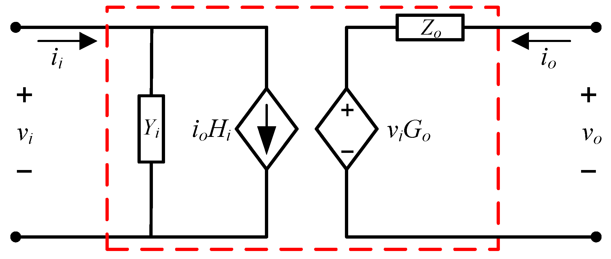
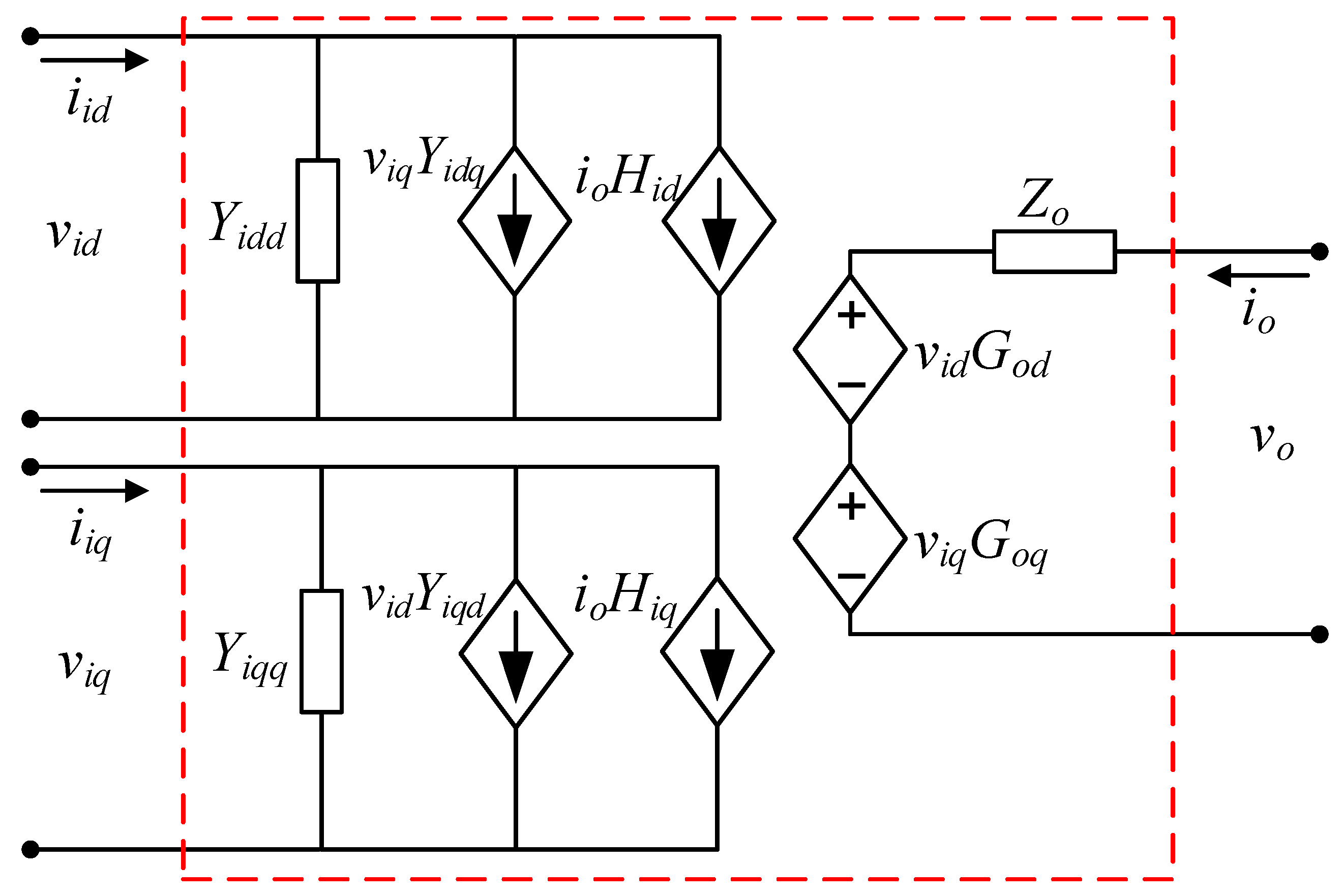
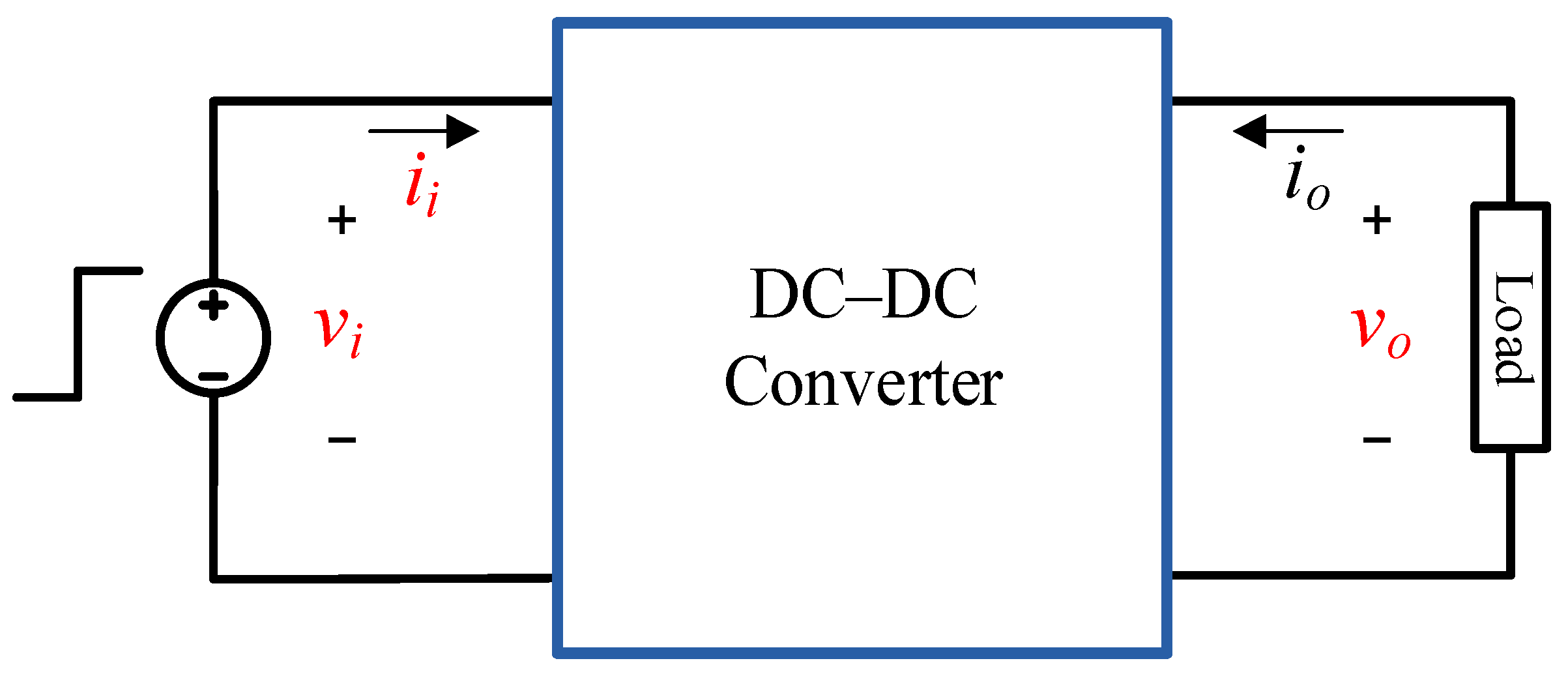
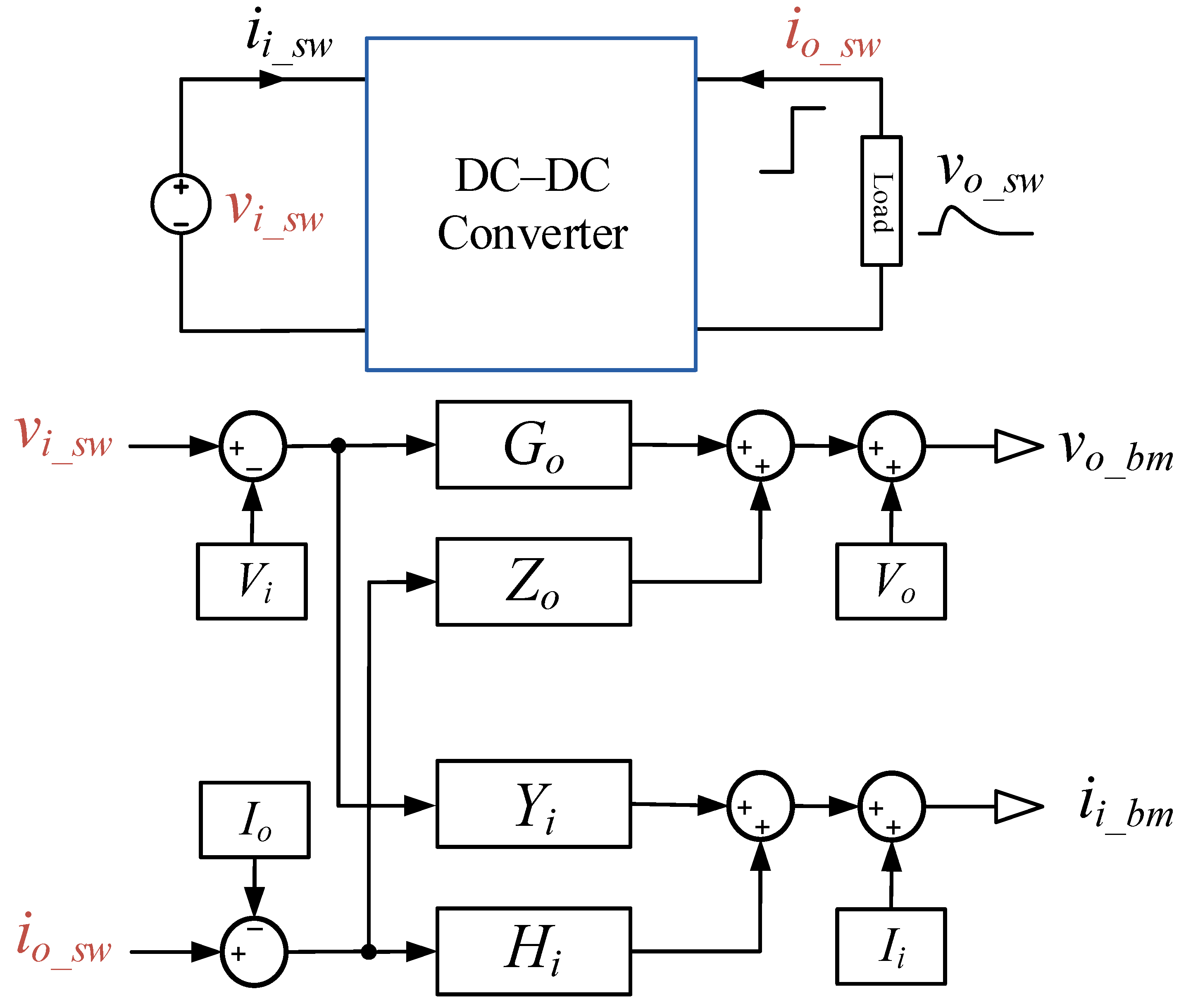
2. Behavioral Modeling for Power Electronic Converters

The two-port network-based behavioral modeling methodology is a hardware dependent approach, that is independent of the prior information regarding the detailed specifications of the converters. It requires the measurement and identification of linear time invariant (LTI) models, also known as g-parameters, introduced in [40], i.e., audiosusceptibility ( G o ) , input admittance ( Y i ) , output impedance ( Z o ) , and back current gain ( H i ) . The two-port network model based on g-parameters for a dc–dc PEC is shown in Figure 2.
For any PEC, the number of transfer functions required to construct its behavioral model is equal to the number of input variables times the number of output variables. As the dc–dc converter consists of two input and two output variables, its behavioral model requires measurement and identification of four transfer functions, as shown in Equation (1) [40].
[ v o i i ] = [ G o Z o Y i H i ] [ v i i o ]
Input voltage and output current ( v i ,   i o ) are the input variable of the two-port network, while the output voltage and input current ( v o ,   i i ) are the output variables of the two-port network.
The same concept used for dc–dc converters is applied for modeling of three-phase ac–dc converters [39]. The input of three-phase ac–dc converters is a three-phase source, so it is a four-port network in d q synchronous frame; however, the output being dc is represented by a two-port network. The g-parameters-based linear model for a three-phase ac–dc converter in d q domain is shown in Figure 3.
The three-phase ac–dc PEC consists of three input and three output variables, therefore its behavioral model requires measurement and identification of nine transfer functions, as shown in Equation (2).
[ v o i i d i i q ] = [ G o d G o q Z o Y i d d Y i d q H i d Y i q d Y i q q H i q ] [ v i d v i q i o ]
The input variables of the g-parameters-based model are the input voltage and output current ( v i d , v i q ,   i o ) , whereas the output voltage and input current ( v o ,   i i d ,   i i q ) are the output variables of the g-parameters based model.

2.1. Acquisition of Measurement Data

In order to measure the g-parameters, either the frequency or the transient response-based method could be employed [30,31,32]. The frequency response-based measurement method is based upon introducing a perturbation in input signals. This perturbation is achieved through an ac sweep signal, generated by a frequency response analyzer. The injection of perturbation in input signal results in small signal changes in the output signal.
In contrast, the transient response-based measurement method does not require any expensive equipment, i.e., a network analyzer. The transient response-based method is based upon introducing a step change in the input signal which results in transient change in the output signal. Once the perturbation has been injected or step change has been introduced, both the input and output frequency or time domain signals are recorded and subsequently used for identification of frequency responses.
The setup to acquire data for the measurement of the output impedance and back current gain of a dc–dc PEC is shown in Figure 4. A certain magnitude step change is applied at the load side of dc–dc PEC. The input signal ( i o ) and the output signals ( v o , i i ) are recorded and subsequently used for the identification of output impedance ( v o / i o ) and back current gain ( i i / i o ) .
The setup to acquire data for the measurement of the audio-susceptibility and input admittance of a dc–dc PEC is shown in Figure 5. A certain magnitude step change is applied at the input voltage of dc–dc PEC. The input signal ( v i ) and the output signals ( v o , i i ) are recorded using an oscilloscope and subsequently used for the identification of audiosusceptibility ( v o / v i ) and input admittance ( i i / v i ) .
The procedure to discuss the identification of transfer functions for dc–dc converters from measurement data is given in [32] via the transient response-based method and in [41] via the frequency response-based method. The complete measurement and identification of g-parameters for a three-phase ac–dc converter via the frequency response-based method can be found in [39]. After the acquisition of measurement data, parametric and non-parametric methods are employed to identify the dynamic models [42]. The order of the identified dynamic model has a very significant role in determining the complexity of the constructed behavioral model. Methodologies have been discussed in the literature to reduce the order of the identified models [41]. Usually, a compromise between model accuracy and simplicity of the model is required. The order of the identified transfer functions should be the lowest value which can provide the highest degree of accuracy. Once the transfer functions are obtained, the behavioral model is built and simulated in Matlab/Simulink (Mathworks, Natick, MA, USA) [43].

2.2. Behavivoral Model Verification

The verification of the developed behavioral model is done by doing the system’s dynamic analysis. First, a switch model of the dc nanogrid-based DES is simulated and its behavioral model is constructed. Then, large signal step disturbance is introduced to the load current or the input voltage of the switch model to perform dynamic analysis. Model verification is performed with the data that is dissimilar from that which is used to build the model [44]. The point to note here is that these large signal step disturbances are introduced to the input–output terminals of the system, i.e., to maintain black-box modeling methodology.

2.2.1. Model Verification for DC–DC Converter

The time domain waveforms of both the input ( v i _ s w , i o _ s w ) and the output ( v o _ s w , i i _ s w ) signals of the switch model of the dc–dc PEC are recorded. Then, the same input signals from the switch model are applied to the constructed behavioral model as shown in Figure 6. Then, the output signals from both, i.e., the switch model ( v o _ s w , i i _ s w ) and the behavioral model ( v o _ b m , i i _ b m ) are compared; in the case that they match closely, this results in verification of the constructed behavioral model. In Figure 6, the capital letters ( V i , I o , V o , I i ) are used to denote the operating point values.

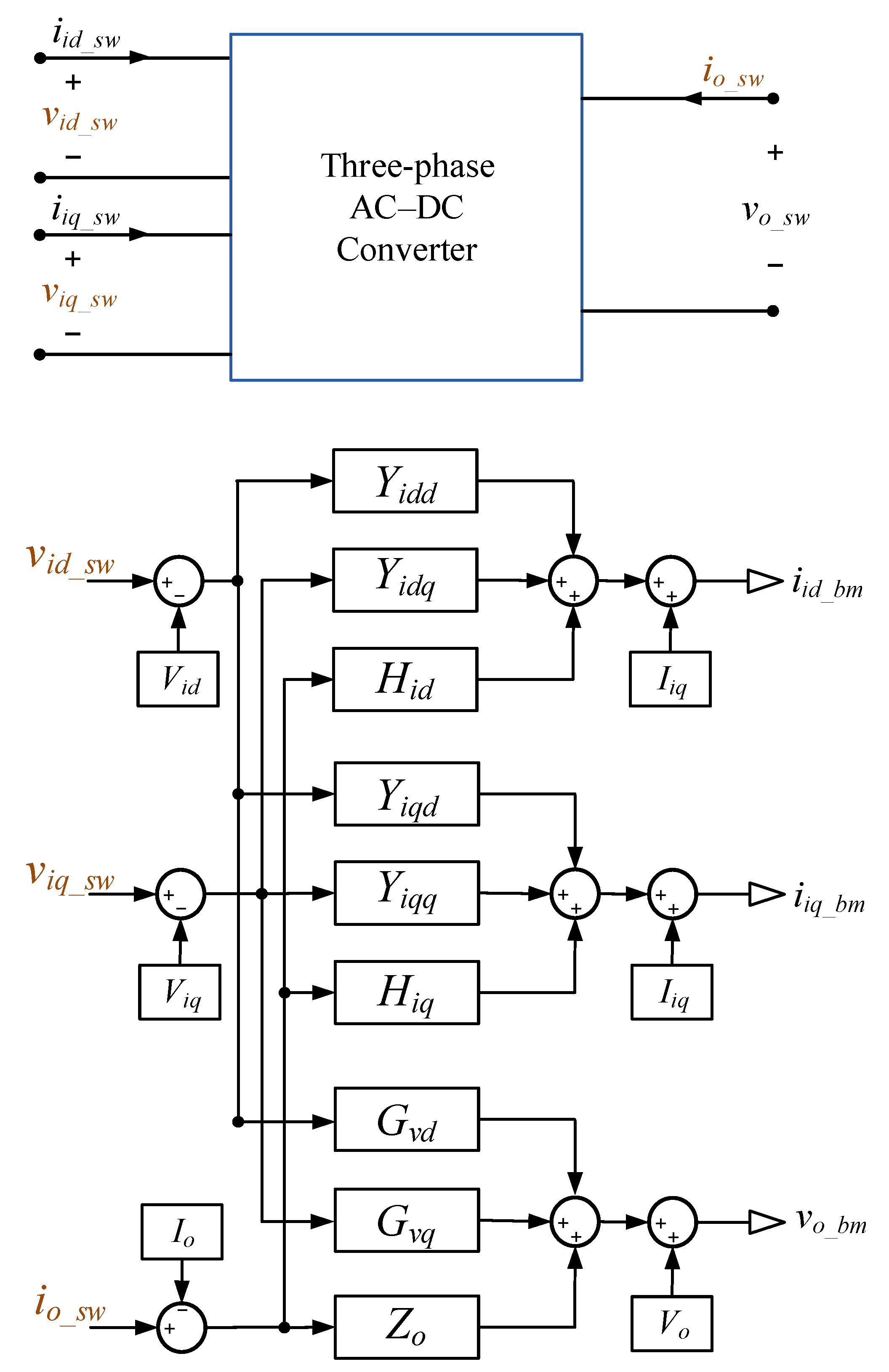
2.2.2. Model Verification for Three-Phase AC–DC Converter

The time domain waveforms of both the input ( v i d _ s w , v i q _ s w , i o _ s w ) and the output ( v o _ s w , i i d _ s w , i i q _ s w ) signals of the switch model of the three-phase PEC are recorded. These input signals from the switch model are applied to the developed behavioral model as shown in Figure 7. Then, the output signals from both, i.e., the switch model ( v o _ s w , i i d _ s w , i i q _ s w ) and the behavioral model ( v o _ b m , i i d _ b m , i i q _ b m ) , are compared; in the case that they match closely, this results in verification of the constructed behavioral model. The capital letters ( V i d , V i q ,   I o , I i d , I i q ,   V o ) are used to denote the operating point values.
The transfer functions required to be measured for constructing the behavioral model of three-phase ac–dc PEC, as shown in Figure 7, are given in Equation (3).
{ G o d = v o v i d | i o = v i q = 0   G o q = v o v i q | i o = v i d = 0   Z o = v o i o | v i d = v i q = 0 Y i d d = i i d v i d | i o = v i q = 0   Y i d q = i i d v i q | i o = v i d = 0   H i d = i i d i o | v i d = v i q = 0 Y i q d = i i q v i d | i o = v i q = 0   Y i q q = i i q v i q | i o = v i d = 0   H i q = i i q i o | v i d = v i q = 0

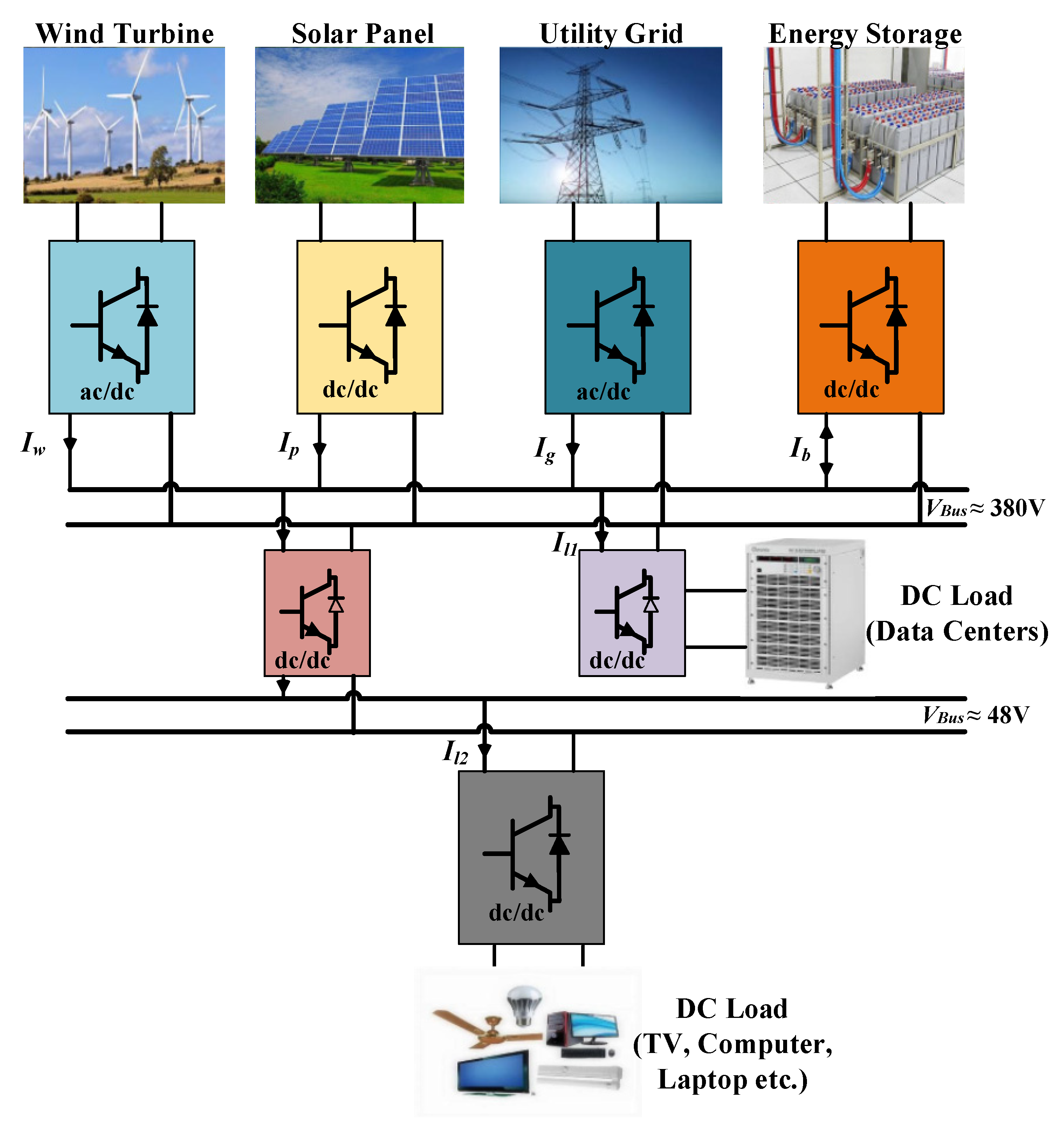
3. DC Nanogrid-based Distributed Energy System

In this section, the behavioral modeling technique has been applied to a complex dc nanogrid-based DES, whose block diagram is shown in Figure 8.
The dc nanogrid system consists of a central 380 V LVdc bus [22], which serves as the interface point for all the sources and loads. The sources include a three-phase voltage source labelled as grid, a renewable energy source in the form of photovoltaic (PV) source, and a battery as a storage device. As mentioned earlier, the 380 V LVdc bus is being proposed by many researchers to become an industry standard [17] for certain loads, i.e., data centers [4,23,24], telecom applications [22,23,24,25], and major household appliances [21,26]. Additionally, the 48 V voltage level is being recommended for certain electronic applications [17,21]. The three-phase voltage source is connected to the LVdc bus via a three-phase ac–dc converter (115 Vrms/380 V) [45]. The PV system is connected to the 3 LVdc bus via a dc–dc boost converter (55/380 V) [46]. The battery is connected to the LVdc bus via a bidirectional dc–dc converter (240/380 V) [47]. Two dc loads are connected, one directly to the LVdc bus [21,26] and the other via a dc–dc buck converter (380/48 V) [17,21]. Table 1 shows the values of different parameters used for the simulation of a dc nanogrid system.
First, the switch model of dc nanogrid-based DES is simulated. The measurement and identification of the g-parameters of various converters of the dc nanogrid system is carried out according to the technique already presented in Section 2.
When a certain magnitude step change is applied in the output current ( i o ) , i.e., load 2, it introduces a step change in the bus current ( i b ) as well. The bus current is the input current of the dc–dc converter connected to load 2, while at the same time it is the output current of the converters interfacing grid, PV and battery to the dc bus. The parameters given in Equation (4) are measured.
{   Z o L 2 = v o i o | v b = 0   H i L 2 =   i b i o | v b = 0     Z o p = v b i b | v i p = 0   H i p =   i i p i b | v i p = 0   Z o b = v b i b | v i b = 0   H i b =   i i b i b | v i b = 0
When a certain magnitude step change is applied in the PV input current ( i i p ) via changing the irradiance level of PV, it introduces a step change in bus voltage as well. The bus voltage is the output voltage of the converters interfacing grid, PV and battery to the dc bus, while at the same time it is the input voltage of the dc–dc converter connected to load 2. The parameters given in Equation (5) are measured.
{   G o L 2 = v o v b | i o = 0   Y i L 2 =   i b v b | i o = 0   G o p = v b v i p | i b = 0   Y i p =   i i p v i p | i b = 0   G o b = v b v i b | i b = 0   Y i b =   i i b v i b | i b = 0

3.1. Model Verification

Once the required transfer functions have been obtained, these are substituted in the behavioral model. The accuracy of the proposed model is verified via applying several test input signals to the switching model of dc nanogrid-based DES and the output signals are recorded. The magnitude of the step change during validation is kept different from the one used during measurement of g-parameters used for the construction of the behavioral model. The same test input signals are introduced to the behavioral model constructed, and comparison of the output of behavioral model is made with that of the switching model. The results are discussed in the next section, in which the green color represents the averaged switch model response and the red color represents the behavioral model’s response.

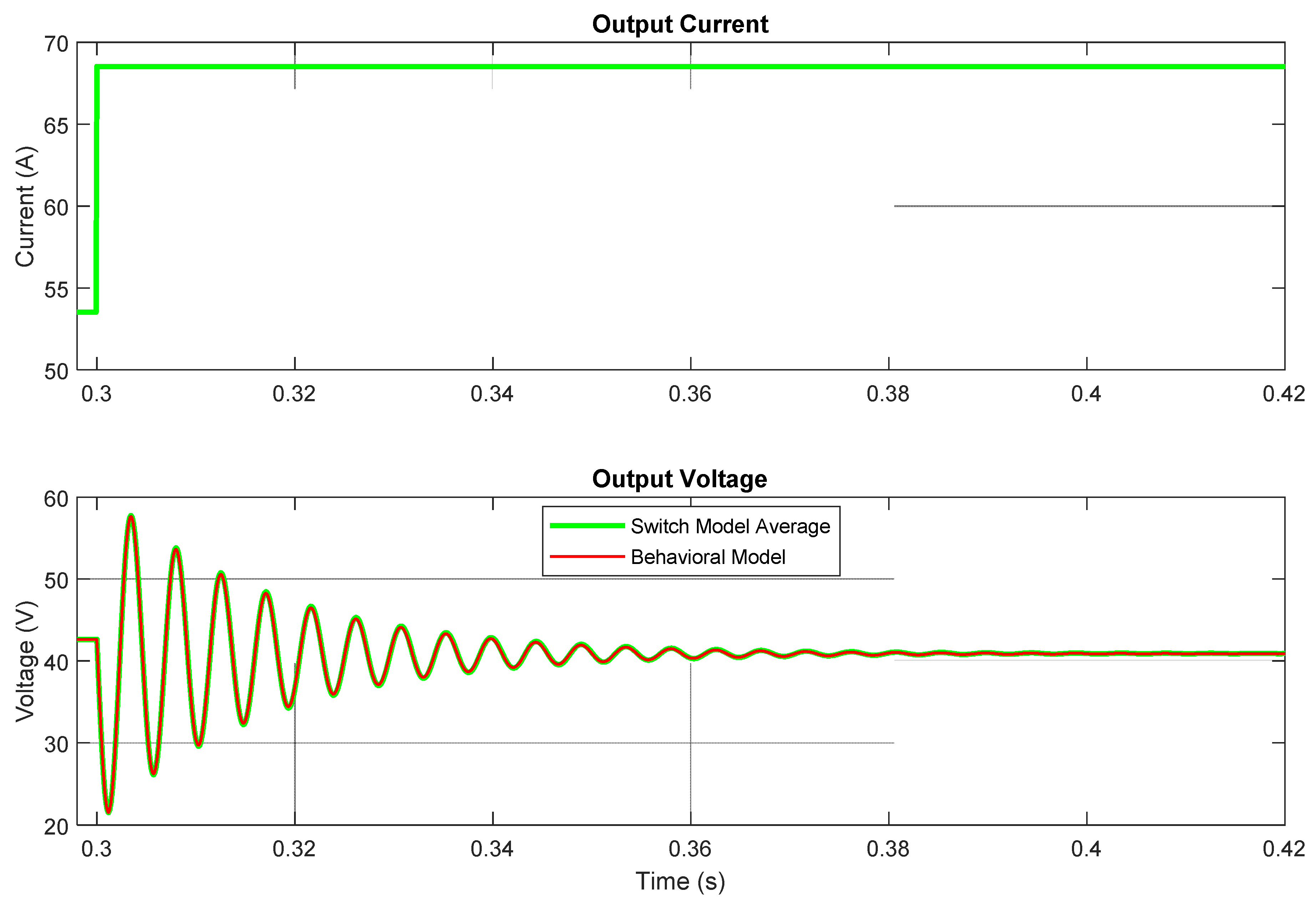
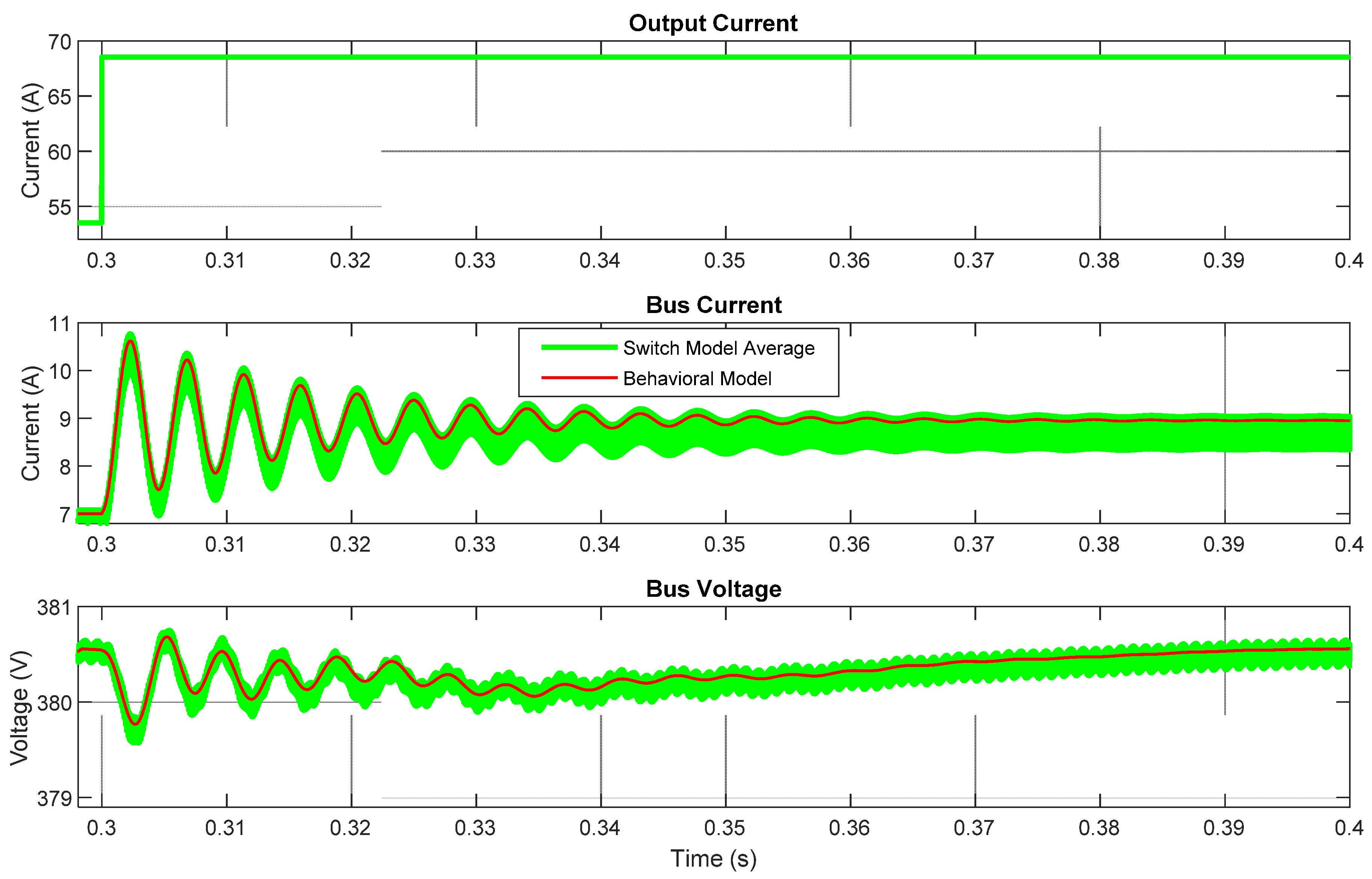
3.1.1. Output Current Step Test

In the first test, a step change is applied in the output current ( i o ) , i.e., load 2. The subsequent figures show the comparison of the switch mode and behavioral model.
When a step change is applied in the output current, the comparison of output voltage waveforms for the switching model and the behavioral model is shown in Figure 9.
When a step change is applied in the output current, the comparison of bus current and bus voltage waveforms for the switching model and the behavioral model is shown in Figure 10.
For the dc–dc buck converter, the roots are 1 × 10 3 ( 1.0639 ± 0.88 i ) , i.e., complex, hence leading to an underdamped (oscillatory) type of response. Furthermore, when a step change is applied in the output current ( i o ) , it introduces disturbance in bus voltage and bus current as well, because it serves as input to the dc–dc buck converter. So, when the step change is introduced in the output current, it results in disturbance in the bus current as well. As the nature of the response of the dc–dc buck converter is underdamped (oscillatory), it results in the similar type of response of bus voltage and bus current. The output current ( i o ) has been increased so it results in an increase in bus current as well, therefore higher levels of oscillation is seen in bus current as compared to bus voltage, which returns to its nominal value after some time.

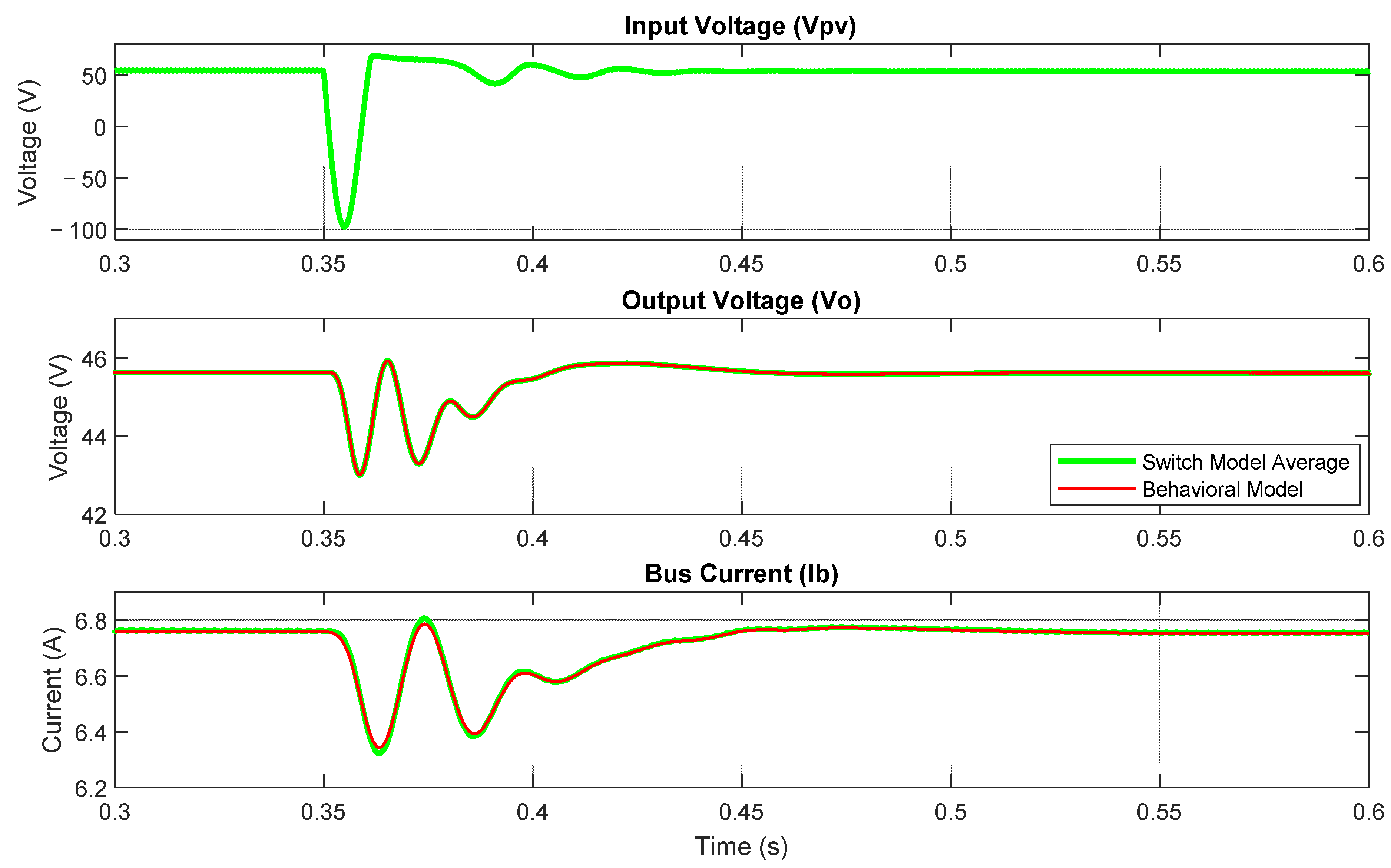
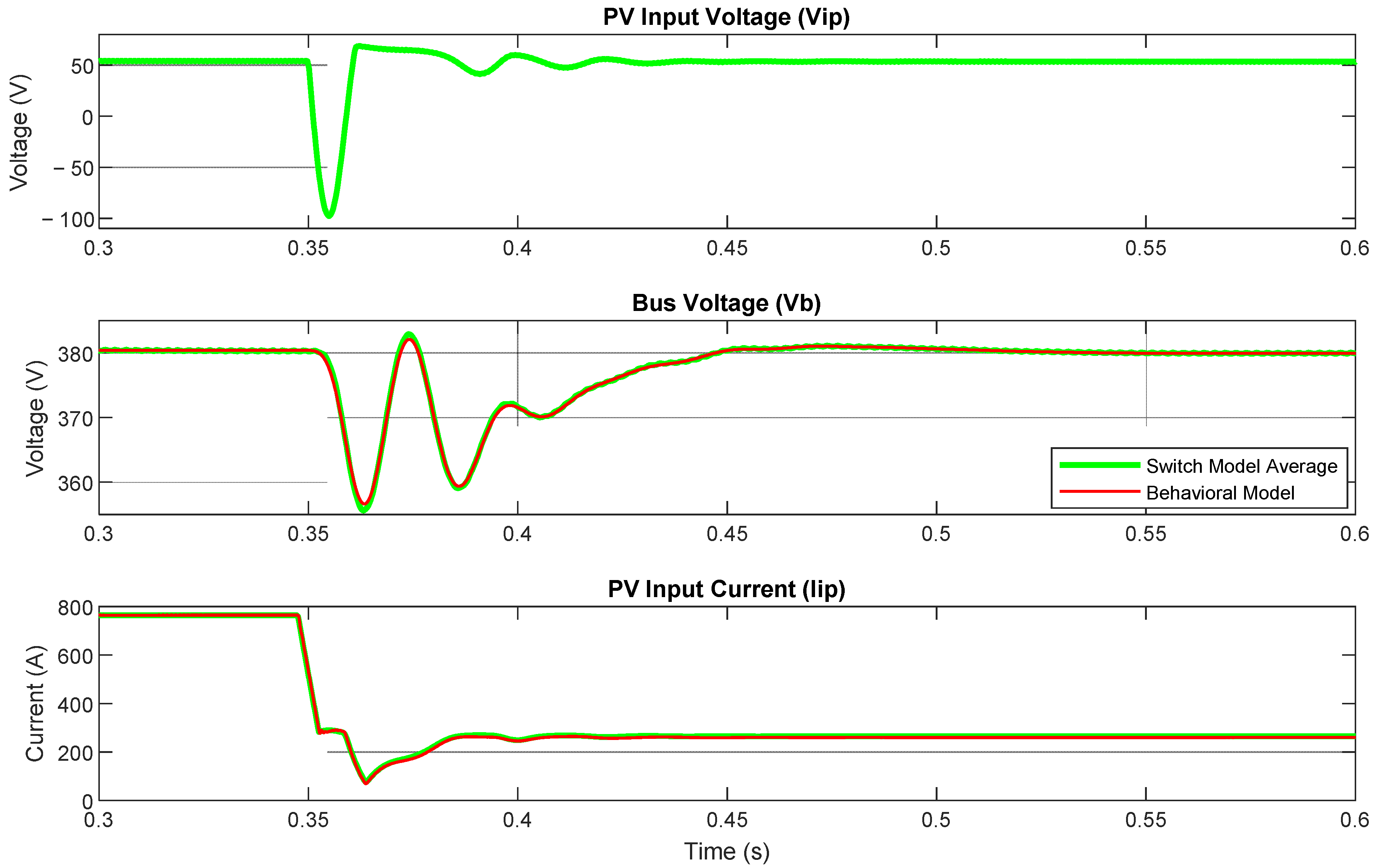
3.1.2. PV Input Current Step Test

In the second test, step change is applied in PV input current via decreasing the irradiance level from 7.8654 W / m 2 to 2.8654 W / m 2 (per module). As the irradiance level has been decreased, it results in the decrease of current from the PV source ( i i p ) , and consequently a reduced power output. The subsequent figures show the comparison of the switch model and the behavioral model. When a step change is applied in the PV generated current, the comparison of bus voltage and PV input current waveforms for the switching model and the behavioral model is shown in Figure 11.
When a step change is applied in the PV input voltage, the comparison of output voltage and bus current waveforms for the switching model and the behavioral model is shown in Figure 12. The results shown in Figure 10, Figure 11 and Figure 12 show that the behavioral model for dc nanogrid-based DES is successfully able to predict the dynamic response of output variables in response to disturbance in the input variables. It shows that the proposed behavioral model for dc nanogrid-based DES has a very good accuracy.
For quantitative comparison of the responses of the switch model and the behavioral model, the root mean square deviation (RMSD) values are computed for the above waveforms. Table 2 shows that the RMSD values are quite small, thus indicating very low error for the behavioral model and thus validating its accuracy. Equation (6) shows the equation used for computation of RMSD values.
The comparison of the switch model’s response is made with the behavioral model’s response for output voltage and input current:
R M S D ( v o swt , v o beh   model ) = x = 1 n ( v o , x swt v o , x beh   model ) 2 n
The comparison of the simulation time for the switch model vs. the behavioral model is presented in Table 3. While computing the simulation time, the simulation configuration parameters, i.e., step size, solver type etc., have been kept same. The comparison shows a remarkable reduction in the simulation time for the behavioral model as compared to the switch model, thus highlighting its advantage over the switch model.

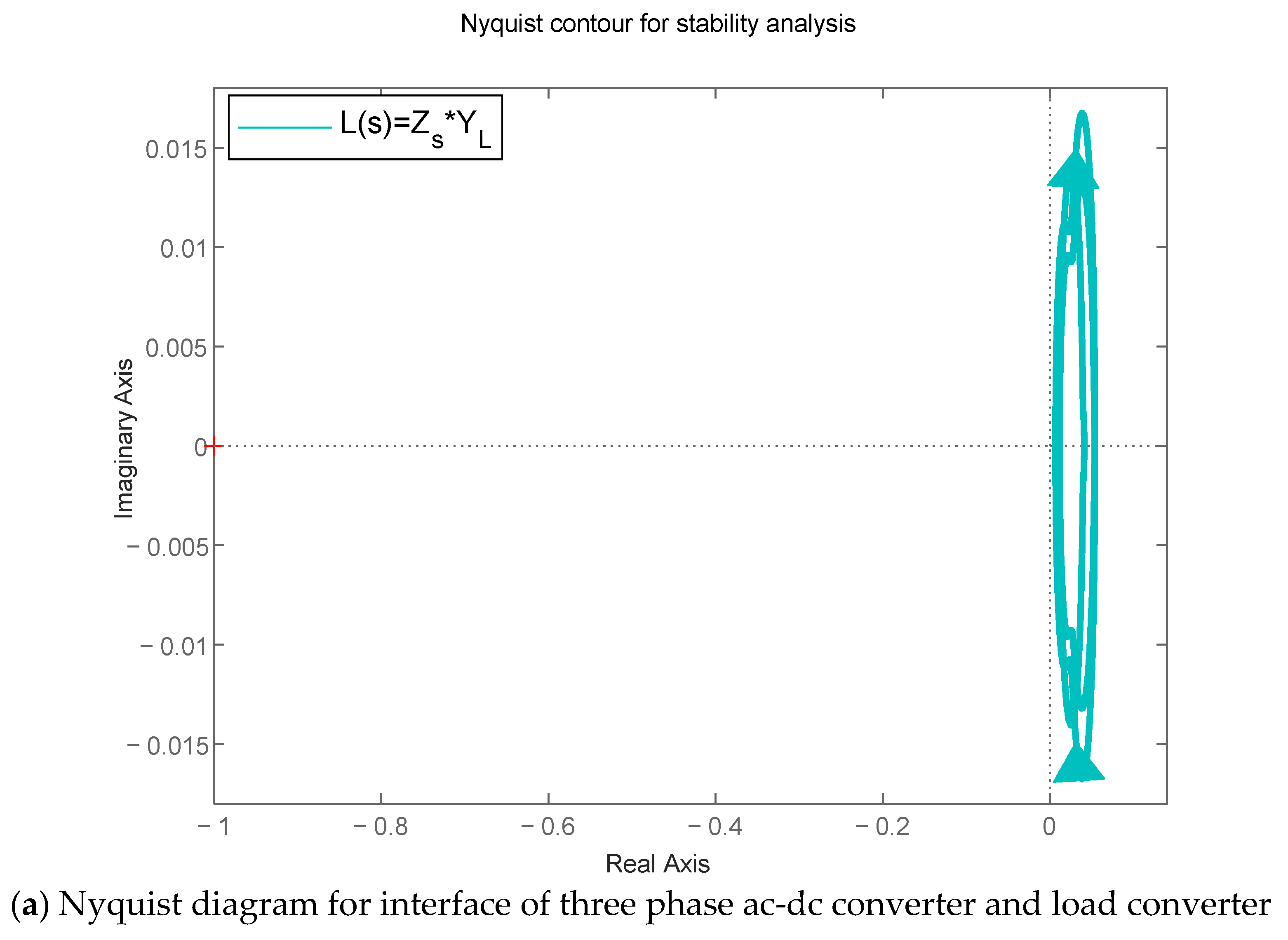
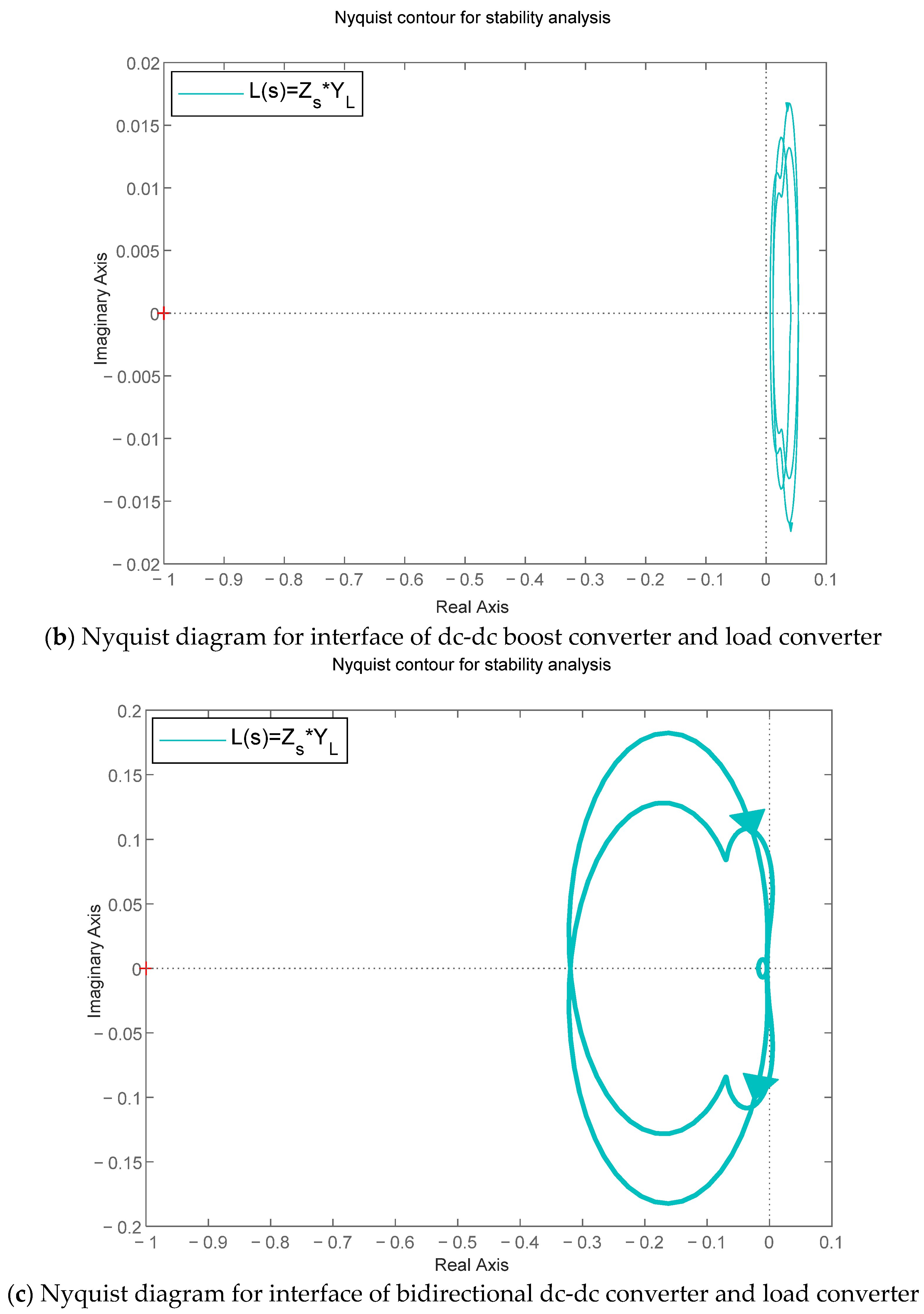
3.1.3. Stability Analysis of dc Nanogrid-Based DES

The integration of various PECs into dc nanogrid-based DES may give rise to issues regarding the whole system’s stability. To address this concern, the stability analysis of the dc nanogrid-based DES is being done using small signal impedance-based models [48,49]. This approach relies upon the measurement of output impedance of the source sub-system and input admittance of the load sub-system [49]. The technique is valid for the small-signal stability analysis of a dc nanogrid-type system, i.e., with multiple interconnected PEC. According to this methodology, if Z s and Y L represent the output impedance of the source sub-system and input admittance of the load sub-system at an interface, the resulting small signal transfer function is as given in Equation (7).
V o ( s ) V i ( s ) = Z L ( s ) Z L ( s ) + Z s ( s ) = 1 1 + Z s ( s )   Z L ( s )  
The system would stable if the impedance ratio Z s ( s ) / Z L ( s ) satisfies the Nyquist criterion. It shows that the system stability depends upon the ratio L ( s ) called the minor loop gain, shown in Equation (8) [50].
L ( s ) = Z s ( s ) Z L ( s ) = Z s ( s )   Y L ( s )
Therefore, the Nyquist stability criterion can be applied to L ( s ) for the stability analysis of two interconnected PEC at a certain interface. In dc nanogrid-based DES shown in Figure 8, the 380 V dc bus serves as an interface point between three source PECs and a load PEC. As the output impedances of the source PECs and the input admittance of the load PEC have already been measured and identified, the same data is used to determine the minor loop gain L ( s ) for the stability analysis at the 380 V dc bus interface. For the three mentioned cases, the Nyquist diagram of the return ratio is given in Figure 13a–c.
For each of the three cases, the non-encirclement of point (−1,0) in the return ratio Nyquist diagram shows a stable operation between the source and load PECs.

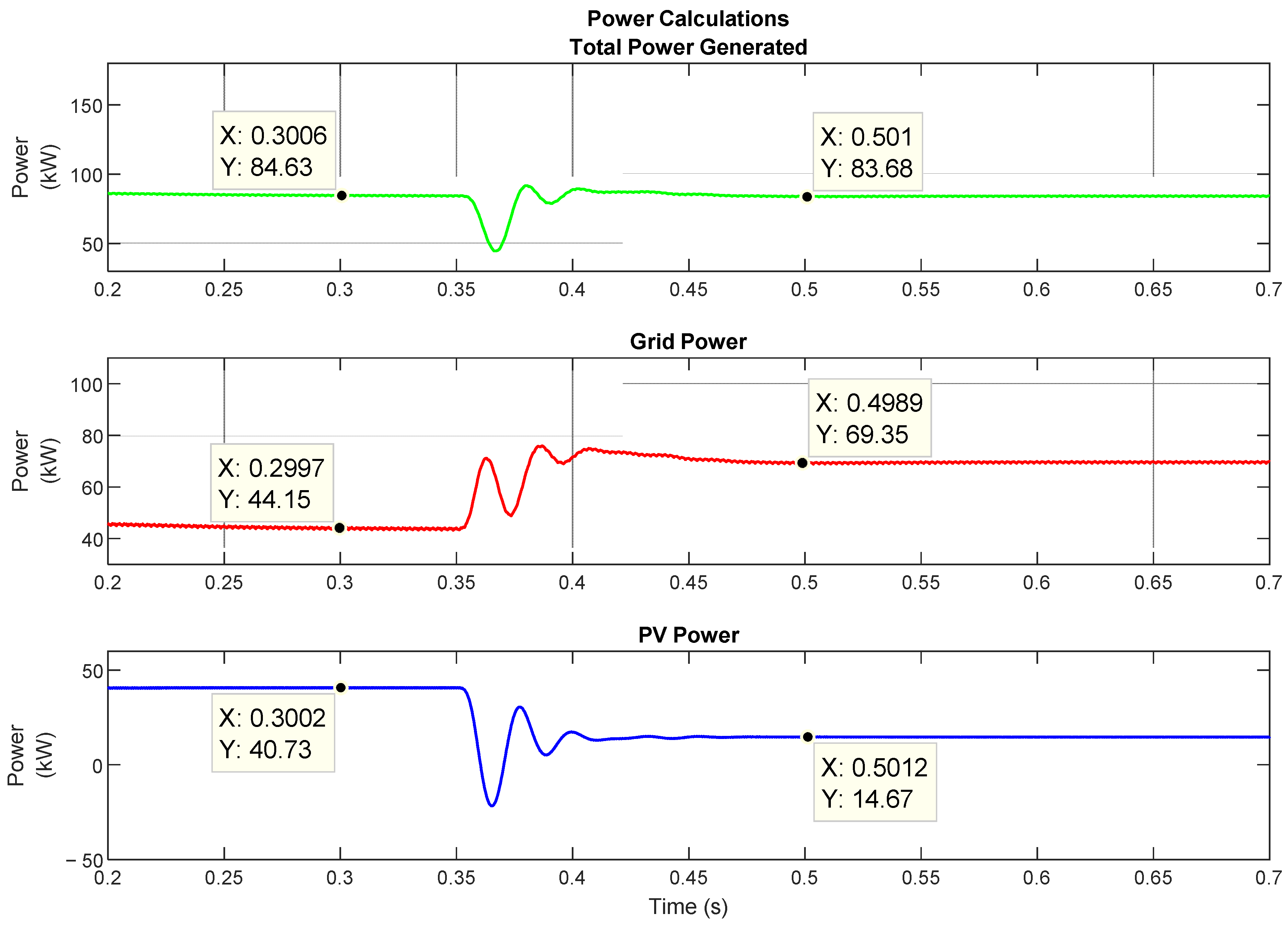
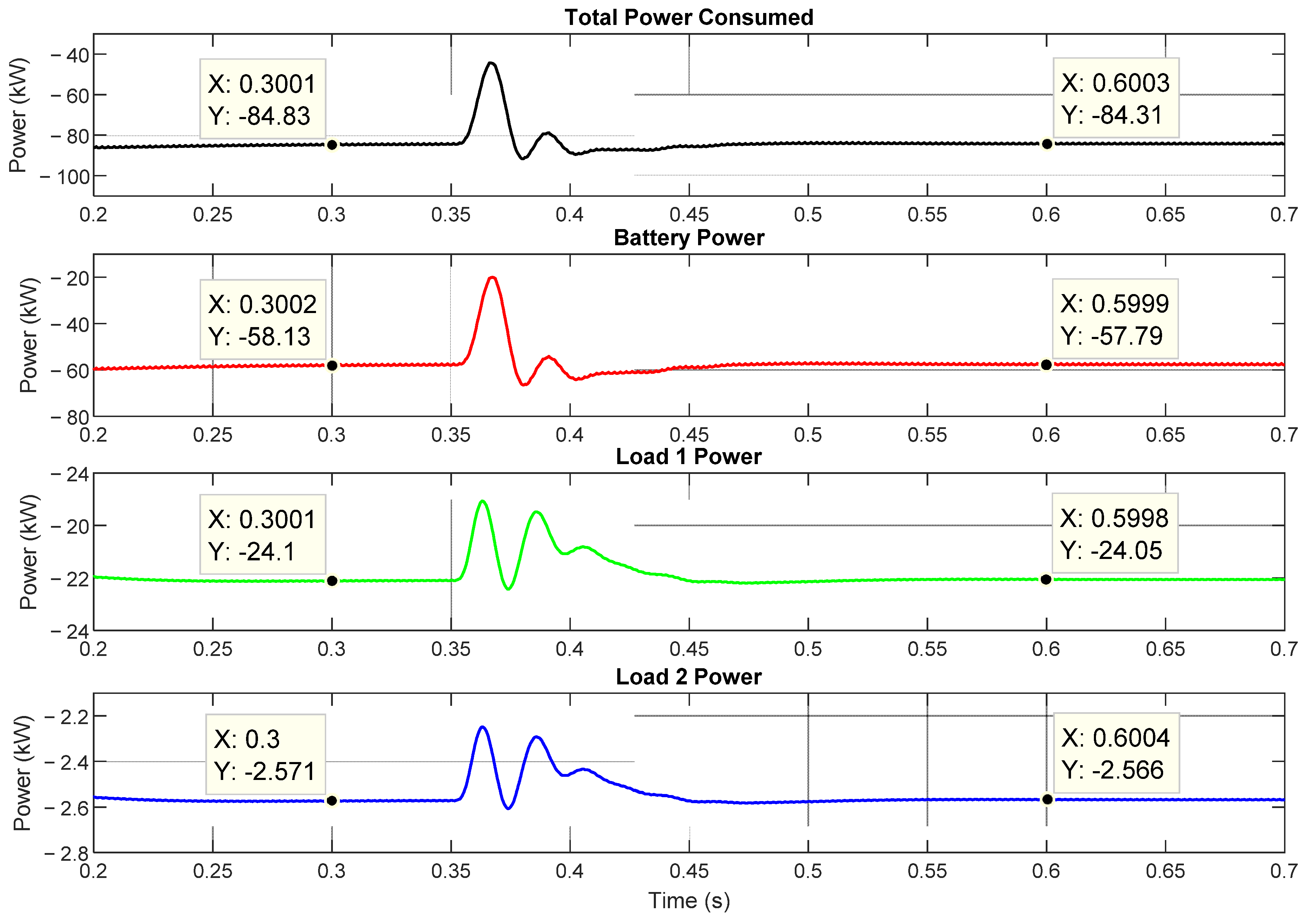
3.1.4. Power Measurements

The acquired data is further utilized to analyze the power generation and consumption by various sources and loads. As shown in Figure 14, a step change is applied in the PV input voltage via changing the irradiance level of PV. As mentioned above, the irradiance level has been decreased leading to reduction in current from PV source, and hence reduction in power output from PV source. Overall, it results in a power drop of 26.06 kW in output of PV, which is compensated by the grid, which increases its power level from 44.15 kW to 69.35 kW to meet the load requirements. Figure 14 shows the total power generated and contribution of grid power and PV power in it. It can be seen that the sum of grid and PV power is equal to the total generated power.
The total power consumed and the share of the battery, load 1 and load 2 is shown in Figure 15. It can be seen that the sum of power consumed by the battery, load 1 and load 2 is equal to the total consumed power.

4. Conclusions

DC nanogrid-based DES are composed of several commercial PEC. The integration of a huge number of PEC in DES can at times negatively influence its dynamic behavior. Due to the interactions among the PEC, their integration is not a straightforward task. In order to ensure an adequate system behavior before the physical set up, suitable electrical models need to be developed. However, the large variety of commercial PEC about which limited information is available make the system level analysis very challenging. One possible way to do the system level analysis is to use behavioral modeling, which is constructed by applying certain perturbation and observing the response on external accessible terminals only. The behavioral modeling approaches have been successfully applied to individual PEC. However, the literature about system level analysis is limited due to increased complexity arising due to interconnection of multiple sources, converters and loads. The paper has proposed the behavioral modeling methodology for application to power electronic converters being integrated to dc nanogrid-based DES for its system level study and dynamic analysis. The behavioral model for various converters are being developed while they are integrated to make dc nanogrid-based DES. The model has been verified by applying certain test signals to the switching and behavioral models and comparing the response of the two. The results justify that the behavioral model is successfully able to predict the dynamic behavior of the dc nanogrid-based DES. Furthermore, the behavioral model is not only successfully able to accurately predict the response of the system at the nominal operating point of the system (before step change), but also when it moves away from its nominal operating point as a result of the application of step change. The quantitative assessment of the behavioral model is carried out via computation of RMSD values, which compares the output of behavioral models with the switch model. As shown in Table 2, the RMSD, i.e., error values for output voltage, bus current and bus voltage parameters (in response to step change in output current), are 0.0791, 0.9810 and 0.8714, respectively. Similarly, the RMSD values for bus voltage, PV input current, output voltage and bus current (in response to step change in PV input voltage) are 0.1938, 0.0412, 0.0012 and 0.0047, respectively. The resulting values show that the deviation of the behavioral model is very low from the switch model, thus validating its accuracy. Additionally, the simulation time for the behavioral model is 87.1% lesser compared to the switch model. This remarkable increase in simulation speed of the behavioral model compared to the switch model highlights the advantage which behavioral modeling would offer in simulation of large and complex systems. Thus, the suitability of behavioral models to model the behavior of the dc nanogrid is justified.

Author Contributions

M.S., H.A. and S.K. conceived and designed the modeling paradigm. M.S., H.A., S.U.J. and B.M.K. performed the experiments, data analysis and implementation of methodology via software simulations. M.S., D.A. and H.A. wrote the original draft of the paper. A.A., A.W. and T.K. provided technical feedback, reviewed and edited the manuscript. Y.J. and H.A. supervised the whole research work. All authors have read and agreed to the published version of the manuscript.

Funding

This research received no external funding.

Conflicts of Interest

The authors declare no conflict of interest.

References

  1. Chen, X.; Hu, S. Distributed generation placement for power distribution networks. J. Circuits Syst. Comput. 2015, 24, 1550009-1–1550009-23. [Google Scholar] [CrossRef]
  2. Muthulakshmi, K.; Sasiraja, R.M.; Kumar, V.S. The proper location and sizing of multiple distributed generators for maximizing stability using PSO. J. Circuits Syst. Comput. 2017, 26, 1750057-1–1750057-20. [Google Scholar] [CrossRef]
  3. Senguttuvan, S.; Vijaykumra, M. Solar photovoltaic system interfaced shunt active power filter for enhancement of power quality in three-phase distribution system. J. Circuits Syst. Comput. 2018, 27, 1850166. [Google Scholar] [CrossRef]
  4. Kumra, D.; Zare, F.; Ghosh, A. DC Microgrid Technology: System Architectures, AC Grid Interfaces, Grounding Schemes, Power Quality, Communication Networks, Applications, and Standardizations Aspect. IEEE Access 2017, 5, 12230–12256. [Google Scholar] [CrossRef]
  5. Fotopoulou, M.; Rakopoulos, D.; Trigkas, D.; Stergiopoulos, F.; Blanas, O.; Voutetakis, S. State of the Art of Low and Medium Voltage Direct Current (DC) Microgrids. Energies 2021, 14, 5595. [Google Scholar] [CrossRef]
  6. Normark, B.; Shivakumar, A.; Welsch, M. DC Power Production and Consumption in Households. In Europe’s Energy Transition-Insights for Policy Making; Elsevier: Amsterdam, The Netherlands, 2017; pp. 237–248. ISBN 978-0-12-809806-6. [Google Scholar]
  7. Ploumpidou, E. Supporting the Transition to DC Micro Grids in the Built Environment 2017; Technische Universiteit Eindhoven: Eindhoven, The Netherlands, 2017. [Google Scholar]
  8. Hakala, T.; Lahdeaho, T.; Komsi, R. LVDC pilot implementation in public distribution network. In Proceedings of the International Conference Electric Distribution (CIRED), Lyon, France, 15–18 June 2015; pp. 1–5. [Google Scholar]
  9. Ullah, S.; Haidar, A.M.A.; Hoole, P.; Zen, H.; Ahfock, T. The Current State of Distributed Renewable Generation, Challenges of Interconnection and Opportunities for Energy Conversion Based DC Microgrids. J. Clean Prod. 2020, 273, 122777. [Google Scholar] [CrossRef]
  10. Gao, L.; Liu, Y.; Ren, H.; Guerrero, J.M. A DC Microgrid Coordinated Control Strategy Based on Integrator Current-Sharing. Energies 2017, 10, 1116. [Google Scholar] [CrossRef] [Green Version]
  11. Park, D.; Candelaria, J.; Ma, L.; Dunn, K. DC ring-bus microgrid fault protection and identification of fault location. IEEE Trans. Power Deliv. 2013, 28, 2574–2584. [Google Scholar] [CrossRef]
  12. Jiang, Z.; Hossain, S.; Huang, H. A distributed, real-time simulation platform for aerospace power system design, testing and evaluation. In Proceedings of the 2016 IEEE National Aerospace and Electronics Conference (NAECON) and Ohio Innovation Summit (OIS), Dayton, OH, USA, 26–29 July 2016; pp. 9–15. [Google Scholar]
  13. Han, D.; Li, S.; Sarlioglu, B. Adoption of wide bandgap technology in hybrid/electric vehicles-opportunities and challenges. In Proceedings of the IEEE International Transportation Electrification Conference (ITEC), Chicago, IL, USA, 22–24 June 2017; pp. 561–566. [Google Scholar]
  14. Miftakhutdinov, R. Overview and design aspects of data- and telecommunication power system to meet latest efficiency and power saving standards and regulations. In Proceedings of the 2011 33rd International Telecommunications Energy Conference (INTELEC), Amsterdam, The Netherlands, 9–13 October 2011. [Google Scholar]
  15. Diaz, E.R.; Vasquez, J.C.; Guerrero, J.M. Intelligent dc homes in future sustainable energy systems: When efficiency and intelligence work together. IEEE Consum. Electron. Mag. 2016, 5, 74–80. [Google Scholar] [CrossRef] [Green Version]
  16. Dragičević, T.; Lu, X.; Vasquez, J.C.; Guerrero, J.M. Dc microgrids-part ii: A review of power architectures, applications, and standardization issues. IEEE Trans. Power Electron. 2016, 31, 3528–3549. [Google Scholar] [CrossRef] [Green Version]
  17. Burmester, D.; Rayudu, R.; Seah, W.; Akinyele, D. A review of nanogrid topologies and technologies. Renew. Sustain. Energy Rev. 2017, 67, 760–775. [Google Scholar] [CrossRef]
  18. Boroyevich, D.; Cvetkovic, I.; Dong, D.; Burgos, R.; Lee, F. Future electronic power distribution systems a contemplative view. In Proceedings of the 2010 12th International Conference on Optimization of Electrical and Electronic Equipment, Brasov, Romania, 20–22 May 2010; pp. 1369–1380. [Google Scholar]
  19. Boroyevich, D.; Cvetkovic, I.; Burgos, R. Intergrid: A future electronic energy network? IEEE J. Emerg. Sel. Top. Power Electron. 2013, 1, 127–138. [Google Scholar] [CrossRef]
  20. Francis, A.; Asensi, R.; Garcia, O.; Prieto, R.; Uceda, J. Modeling electronic power converters in smart dc microgrids—An overview. IEEE Trans. Smart Grid 2017, 9, 6274–6287. [Google Scholar] [CrossRef]
  21. Cvetkovic, I.; Dong, D.; Zhang, W.; Jiang, L.; Boroyevich, D.; Lee, F.; Mattavelli, P. A Testbed for Experimental Validation of a Low-voltage DC Nanogrid for Buildings. In Proceedings of the International Power Electronics and Motion Control Conference EPE-PEMC, Novi Sad, Serbia, 4–6 September 2012; pp. 1–8. [Google Scholar]
  22. AlLee, G.; Tschudi, W. Edison redux: 380 Vdc brings reliability and efficiency to sustainable data centers. IEEE Power Energy Mag. 2012, 10, 50–59. [Google Scholar] [CrossRef]
  23. Pratt, A.; Kumar, P.; Aldridge, T.V. Evaluation of 400V DC distribution in telco and data centers to improve energy efficiency. In Proceedings of the 29th International Telecommunications Energy Conference, Rome, Italy, 30 September–4 October 2007; pp. 32–39. [Google Scholar]
  24. Hirose, K. Consideration of voltage range of a 380 VDC distribution system for international standardization. In Proceedings of the 35th International Telecommunications Energy Conference, Smart Power Efficiency (INTELEC), Hamburg, Germany, 13–17 October 2013; pp. 1–6. [Google Scholar]
  25. Inamori, J.; Hoshi, H.; Tanaka, T.; Babasaki, T.; Hirose, K. 380-VDC power distribution system for 4-MW-scale cloud facility. In Proceedings of the 2014 IEEE 36th International Telecommunications Energy Conference (INTELEC), Vancouver, BC, Canada, 28 September–2 October 2014; pp. 1–8. [Google Scholar]
  26. Lucia, O.; Cvetkovic, I.; Boroyevich, D.; Mattavelli, P.; Lee, F. Design of Household Appliances for DC-Based Nanogrid System: An Induction Heating Cooktop Study Case. In Proceedings of the 2013 Twenty-Eighth Annual IEEE Applied Power Electronics Conference and Exposition (APEC), Long Beach, CA, USA, 17–21 March 2013; pp. 1576–1583. [Google Scholar]
  27. Emadi, A. Modeling and analysis of multiconverter dc power electronic systems using the generalized state-space averaging method. IEEE Trans. Ind. Electron. 2004, 51, 661–668. [Google Scholar] [CrossRef]
  28. Mocci, A.; Serpi, A.; Marongiu, I.; Gatto, G. Enhanced modeling of dc-dc power converters by means of averaging technique. In Proceedings of the 40th Annual Conference of the IEEE Industrial Electronics Society (IECON), Dallas, TX, USA, 29 October–1 November 2014; pp. 5101–5107. [Google Scholar]
  29. Oliver, J.A.; Prieto, R.; Romero, V.; Cobos, J.A. Behavioral modeling of DC-DC converters for large-signal simulation of distributed power systems. In Proceedings of the 21st Annual IEEE Applied Power Electronics Conference and Exposition (APEC’06), Dallas, TX, USA, 19–23 March 2006. [Google Scholar]
  30. Arnedo, L.; Burgos, R.; Wang, F.; Boroyevich, D. Black-box terminal characterization modeling of DC-to-DC Converters. In Proceedings of the 22nd Annual IEEE Applied Power Electronics Conference and Exposition (APEC’07), Anaheim, CA, USA, 25 February–1 March 2007. [Google Scholar]
  31. Cvetkovic, I.; Boroyevich, D.; Mattavelli, P.; Lee, F.C.; Dong, D. Nonlinear, hybrid terminal behavioral modeling of a dc-based nanogrid system. In Proceedings of the 26th Annual IEEE Applied Power Electronics Conference and Exposition (APEC), Orlando, FL, USA, 6–11 March 2011. [Google Scholar]
  32. Valdivia, V.; Barrado, A.; Lazaro, A.; Zumel, P.; Raga, C. Easy modeling and identification procedure for “black box” behavioral models of power electronics converters with reduced order based on transient response analysis. In Proceedings of the 24th Annual IEEE Applied Power Electronics Conference and Exposition (APEC), Washington, DC, USA, 15–19 February 2009. [Google Scholar]
  33. Francis, A.; Asensi, R.; Garcia, O.; Prieto, R.; Uceda, J. Black-box small-signal structure for single-phase and three-phase electric vehicle battery chargers. IEEE Access 2020, 8, 170496–170506. [Google Scholar]
  34. Cho, B.H. Modeling and Analysis of Spacecraft Power Systems. Ph.D. Thesis, Virginia Polytechnic Institute and State University, Blacksburg, Virginia, 1985. [Google Scholar]
  35. Ali, H.; Zheng, X.; Zaman, H.; Liu, H.; Wu, X. Behavioral Modeling for parallel and cascade connected dc-dc converters. J. Circuits Syst. Comput. 2019, 28, 1950058-1–1950058-17. [Google Scholar] [CrossRef]
  36. Gong, H.; Yang, D.; Wang, X. Identification of the DQ impedance model for three-phase power converter considering the coupling effect of the grid impedance. In Proceedings of the 2019 IEEE Applied Power Electronics Conference and Exposition (APEC), Anaheim, CA, USA, 17–21 March 2019; pp. 120–126. [Google Scholar]
  37. Valdivia, V.; Lazaro, A.; Barrado, A.; Zumel, P.; Fernandez, C.; Sanz, M. Black-Box Modeling of Three-Phase Voltage Source Inverters for System-Level Analysis. IEEE Trans. Ind. Electron. 2012, 59, 3648–3662. [Google Scholar] [CrossRef]
  38. Guarderas, G.; Frances, A.; Asensi, R.; Uceda, J. Large-signal blackbox behavioral modeling of grid-supporting power converters in AC microgrids. In Proceedings of the 2017 IEEE 6th International Conference on Renewable Energy Research and Applications (ICRERA), San Diego, CA, USA, 5–8 November 2017; pp. 153–158. [Google Scholar]
  39. Ali, H.; Liu, H.; Zheng, X.; Gao, P.; Zaman, H. Frequency response based behavioral modeling verification for three phase AC-DC converter. In Proceedings of the 43rd Annual Conference of the IEEE Industrial Electronics Society, Beijing, China, 29 October–1 November 2017; pp. 4908–4912. [Google Scholar]
  40. Maranesi, P.G.; Tavazzi, V.; Varoli, V. Two-port characterization of PWM voltage regulators at low frequencies. IEEE Trans. Ind. Electron. 1988, 35, 444–450. [Google Scholar] [CrossRef]
  41. Ali, H.; Zheng, X.; Wu, X.; Zaman, H.; Khan, S. Reduced Order Identification and Stability Analysis of DC-DC Converters. J. Power Electron. 2017, 17, 453–463. [Google Scholar] [CrossRef] [Green Version]
  42. Ljung, L. Integrated frequency-time domain tools for system identification. In Proceedings of the American Control Conference, Boston, MA, USA, 30 June–2 July 2004. [Google Scholar]
  43. MathWorks. Available online: http://www.mathworks.com (accessed on 5 November 2020).
  44. Ljung, L. System Identification—Theory for the User, 2nd ed.; Prentice Hall: Upper Saddle River, NJ, USA, 1999. [Google Scholar]
  45. Chen, F.; Burgos, R.; Boroyevich, D.; Zhang, X. Low-Frequency Common-Mode Voltage Control for Systems Interconnected with Power Converters. IEEE Trans. Ind. Electron. 2017, 64, 873–882. [Google Scholar] [CrossRef]
  46. Liang, Y.; Zhang, H.; Du, M.; Sun, K. Parallel Coordination Control of Multi-Port DC-DC Converter for Stand-Alone Photovoltaic-Energy Storage Systems. CPSS Trans. Power Electron. Appl. 2020, 5, 235–241. [Google Scholar] [CrossRef]
  47. She, X.; Huang, A.Q.; Lukic, S.; Baran, M.E. On Integration of Solid-State Transformer with Zonal DC Microgrid. IEEE Trans. Smart Grid 2012, 3, 975–985. [Google Scholar] [CrossRef]
  48. Wildrick, C.M.; Lee, F.C.; Cho, B.H.; Choi, B. A method of defining the load impedance specification for a stable distributed power system. IEEE Trans. Power Electron. 1995, 10, 280–285. [Google Scholar] [CrossRef]
  49. Sun, J. Small-signal methods for AC distributed power systems-A review. IEEE Trans. Power Electron. 2009, 24, 2545–2554. [Google Scholar]
  50. Middlebrook, R.D. Input Filter Considerations in Design and Application of Switching Regulators. In Proceedings of the IEEE Industrial Applications Society Annual Meeting, Chicago, IL, USA, 11–14 October 1976; pp. 366–382. [Google Scholar]
Figure 1. Configuration of direct current (dc) nanogrid based distributed energy system (DES) for future residential applications [20].
Energies 14 07904 g001
Figure 2. Two-port network model based on g-parameters for dc–dc power electronic converter (PEC).
Energies 14 07904 g002
Figure 3. The g-parameters-based model for three-phase ac–dc PEC.
Energies 14 07904 g003
Figure 4. Load current step change-based measurement setup for output impedance and back current gain.
Energies 14 07904 g004
Figure 5. Input voltage step change-based measurement setup for input admittance and audiosusceptibility.
Energies 14 07904 g005
Figure 6. Behavioral model verification for the dc–dc converter.
Energies 14 07904 g006
Figure 7. Behavioral model for the three-phase ac–dc converter.
Energies 14 07904 g007
Figure 8. Block diagram of dc nanogrid-based distributed energy system.
Energies 14 07904 g008
Figure 9. Output voltage waveforms comparison for step change in output current.
Energies 14 07904 g009
Figure 10. Bus current and bus voltage waveforms comparison for step change in output current.
Energies 14 07904 g010
Figure 11. Bus voltage and PV input current waveforms comparison for step change in PV input voltage.
Energies 14 07904 g011
Figure 12. Output voltage and bus current waveforms comparison for step change in PV input voltage.
Energies 14 07904 g012
Figure 13. Stability analysis via Nyquist diagram.
Energies 14 07904 g013aEnergies 14 07904 g013b
Figure 14. Total power generated and contribution of grid power and PV power, before and after the step change.
Energies 14 07904 g014
Figure 15. Total power consumed and the share of battery, load 1 and load 2, before and after the step change.
Energies 14 07904 g015
Table 1. Simulation parameters of dc nanogrid-based DES.
Parameters Input   Voltage   ( V i n ) Switching   Frequency   ( f ) Filter   Inductor   ( L ) Capacitor   ( C ) Output Voltage ( V o )
DC–DC Boost Converter55 V 10 kHz 1 mH 2500 μ F 380 V
Bidirectional Converter240 V 10 k Hz 10 μ H 150 μ F 380 V
DC–DC Buck Converter380 V 100 k Hz 1 mH 520 μ F 48 V
Table 2. Simulation parameters of dc nanogrid-based DES.
Figure No.ParameterMean Square Error (MSE)
Figure 9Output Voltage0.0791
Figure 10Bus Current0.9810
Bus Voltage0.8714
Figure 11Bus Voltage0.1938
PV Input Current0.0412
Figure 12Output Voltage0.0012
Bus Current0.0047
Table 3. Simulation time comparison for the switch model and behavioral model of dc nanogrid-based DES.
Switch ModelBehavioral ModelPercentage Decrease
140 s18 s87.1%
Publisher’s Note: MDPI stays neutral with regard to jurisdictional claims in published maps and institutional affiliations.

