Article

Symmetrical Cascaded Switched-Capacitor Multilevel Inverter Based on Hybrid Pulse Width Modulation

1
School of Mechanical Engineering and Automation, Harbin Institute of Technology, Shenzhen 518055, China
2
School of Automation, Guangdong University of Technology, Guangzhou 510006, China
*
Author to whom correspondence should be addressed.
Energies 2021, 14(22), 7643; https://doi.org/10.3390/en14227643
Submission received: 12 October 2021 / Revised: 6 November 2021 / Accepted: 11 November 2021 / Published: 15 November 2021

Abstract

:
Multilevel inverters have been widely used in various industrial applications such as renewable energy generation and electric vehicles. An improved circuit of symmetrical cascaded switched-capacitor multilevel inverter is proposed so that the reactive power is absorbed by its power supply instead of capacitors. Then, a special hybrid pulse width modulation strategy combing level-shifted pulse width modulation (LS-PWM) and phase-shifted pulse width modulation (PS-PWM) was developed for the inverter. With this modulation algorithm, the power between cascaded units is automatically balanced, and the voltage of the capacitor in each unit is also automatically balanced to the dc input voltage. In addition, the optimized capacitor voltage ripple makes it possible to use a smaller capacitor to produce a better output voltage waveform. Theoretical analysis, simulation and experimental results show that the equivalent switching frequency of the cascaded multilevel inverter is twice the original frequency so that the output voltage harmonics are only distributed near even multiples of the carrier frequency.

1. Introduction

Recently, multilevel inverters have been widely used in photovoltaic power generation, energy vehicles and high voltage DC (HVDC) transmission since it not only offers the advantage of low voltage stress across switching devices on the occasion of high voltage application but also generates a sinusoidal output waveform with reduced harmonic distortion at low switching frequency [1,2].
Basically, multilevel inverters can be categorized into three types: diode-clamped, capacitor-clamped, and cascaded H-bridge. One dc voltage source is equipped in the diode-clamped and capacitor-clamped multilevel inverter, which utilizes diodes or capacitors to divide the dc source voltage into multiple voltage levels. A large number of power switches, complex switching strategies and capacitor voltage balancing control are required for the clamped-type multilevel inverter [3,4,5]. On the other side, the cascaded H-bridge multilevel inverter has less switch voltage stress, and it is easy to realize the modular design. However, multiple isolated dc sources are required [6,7].
In order to overcome the limitation of the conventional multilevel inverters, a variety of novel topologies have been proposed, such as modular multilevel converter (MMC) [8,9], Z-source inverter [10,11], switched boost inverter [12,13], switched-capacitor (SC) inverter [14,15,16,17,18,19,20,21,22,23,24], etc. The switched-capacitor multilevel inverter has especially gained more popularity because of its self-voltage balancing and boosting ability. In [17,18], by constructing an H-shaped SC cell with three switches and two voltage sources (dc sources or capacitors), the voltage sources are connected in series or parallel by controlling the three switches appropriately, thus more numbers of voltage levels are generated. In [19], two switches of an SC cell are replaced by two diodes so that the modulation circuit design is simplified. In [20], a new SC cell consisting of four switches, two diodes and two capacitors is proposed to produce more output voltage levels. A single back-end H-bridge inverter is connected in [17,18,19,20], and the voltage stress of the H-bridge power switches is large, which is equal to the maximum voltage level of the dc bus.
In order to reduce the voltage stress of the H-bridge switches and the number of isolated dc voltage sources, the switched-capacitor techniques are integrated into a cascaded H-bridge multilevel inverter in [21] by adding bidirectional switches between H bridges. Most of the dc voltage sources in the cascaded multilevel inverter are replaced by capacitors, which are charged by a single dc source with the help of bidirectional switches. Further, a low-voltage SC cell and a high-voltage SC cell consisting of seven switches, four capacitors and two diodes are inserted into the dc sides of two cascaded H-bridges to generate more output voltage levels [22]; however, the modulation for power switches is rather complex.
A simple SC cell, consisting of two switches, one diode and one capacitor, is embedded between the dc power supply and H-bridge [23,24]. With the SC cell, two voltage levels in the dc bus and five voltage levels in the output of the H-bridge are obtained. Nevertheless, when reactive power flows from the inductive load to the input, the backflow current would keep charging the capacitor in the SC cell due to the existence of the diode. Thus, it is possible that the capacitor voltage reaches far beyond the dc source voltage when dealing with large reactive power. In addition, symmetrical phase-shift modulation in [23] leads to a power imbalance between cascaded units. Different dc voltage source values are assigned in [24] to produce the maximum number of voltage levels at the output, which aggravates the problem of the power imbalance between cascaded units.
In this paper, the diode of the SC cell in [23,24] is replaced by a power switch, realizing a bidirectional current flow and thus improving the reactive power capability of the inverter. As a result, each cascaded unit involves one capacitor and seven transistors as well as one dc source. More output levels can be obtained by cascading multiple units. Besides, a hybrid pulse width modulation combining level-shifted pulse width modulation (LS-PWM) and phase-shifted pulse width modulation (PS-PWM) was developed for the symmetrical cascaded switched-capacitor multilevel inverter. With this modulation algorithm, the power between cascaded units as well as the voltage of the capacitor in the SC cell is automatically balanced, and the capacitor voltage ripple is effectively minimized. In summary, with the hybrid pulse width modulation, the proposed cascaded SC multilevel inverter has the following highlights:
Self-balanced capacitor voltages;
Self-balanced power among cascaded SC cells;
Reduced capacitor voltage ripple;
Enhanced reactive power capability.

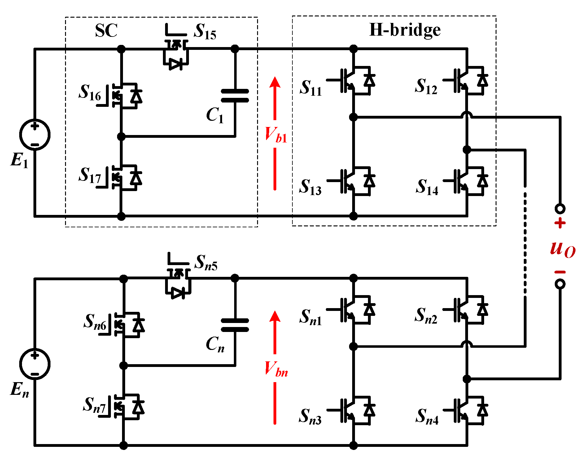
2. Cascaded Switched-Capacitor Multilevel Inverter

2.1. Circuit Description

Figure 1 shows a switched-capacitor multilevel inverter cascaded by n units, and every unit consists of a dc voltage source Ei (i = 1, 2, …, n), an SC cell, and an H-bridge.
The main difference between Figure 1 and the proposed circuit in [23] is that the charging diode of SC is replaced by MOSFET (Si5). As mentioned above, the reactive power capability of the inverter can be improved, and the system power loss can also be significantly reduced since the conduction loss of a MOSFET is much smaller than that of a diode, especially when the charging current is large in low voltage side.

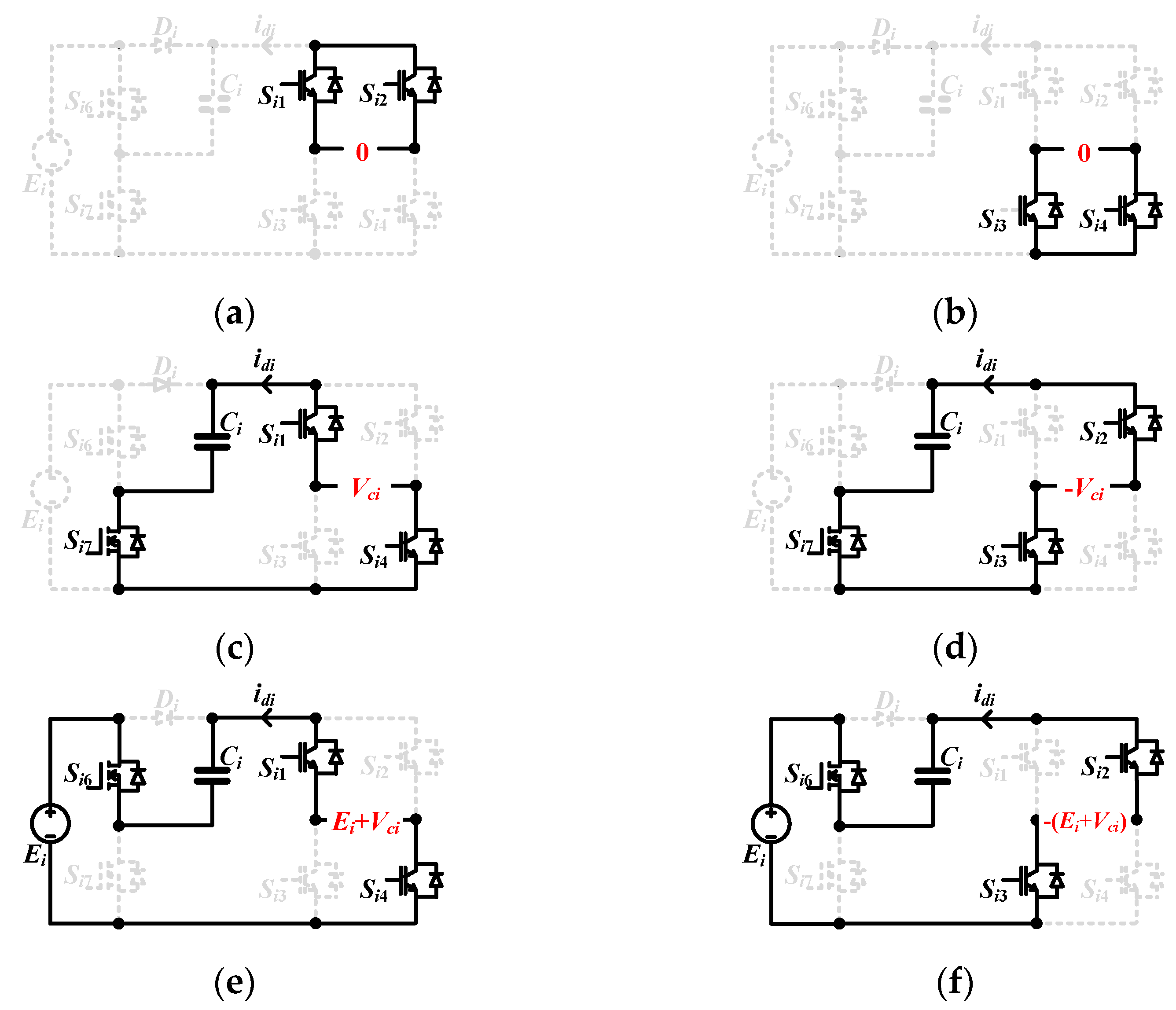
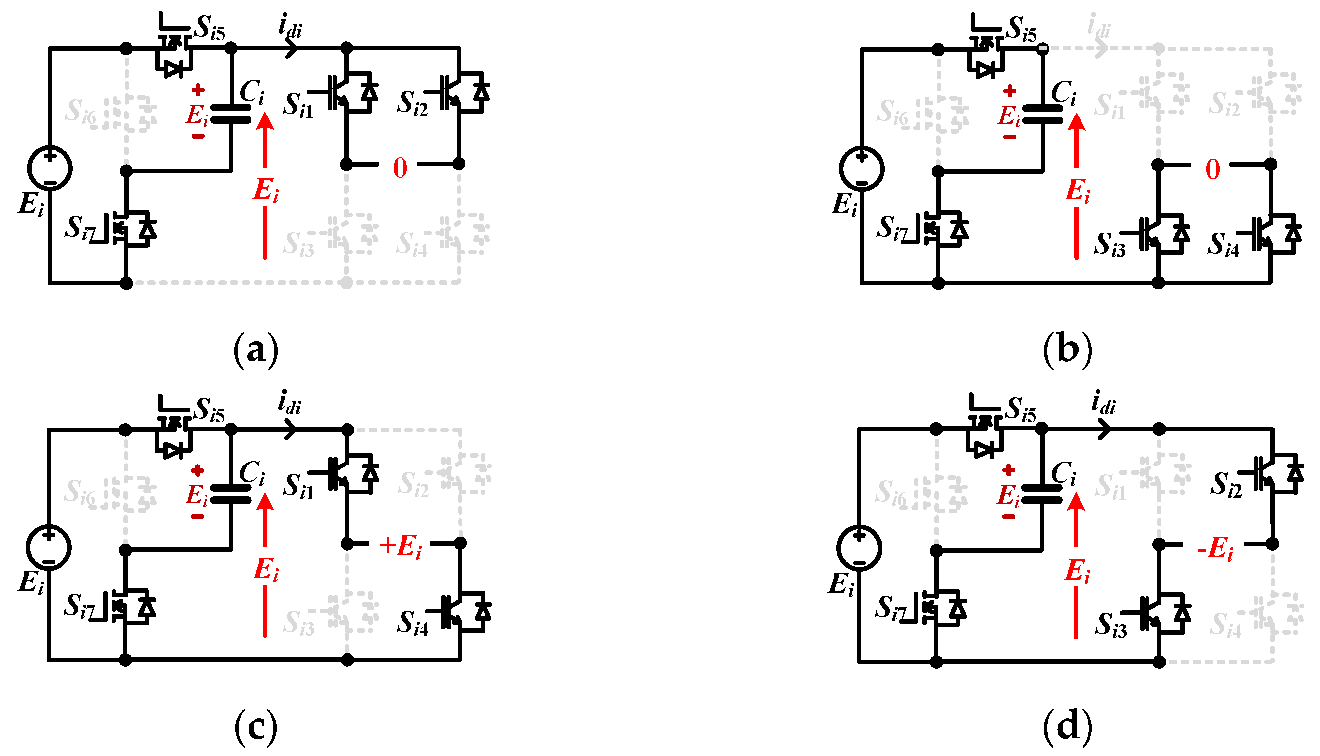
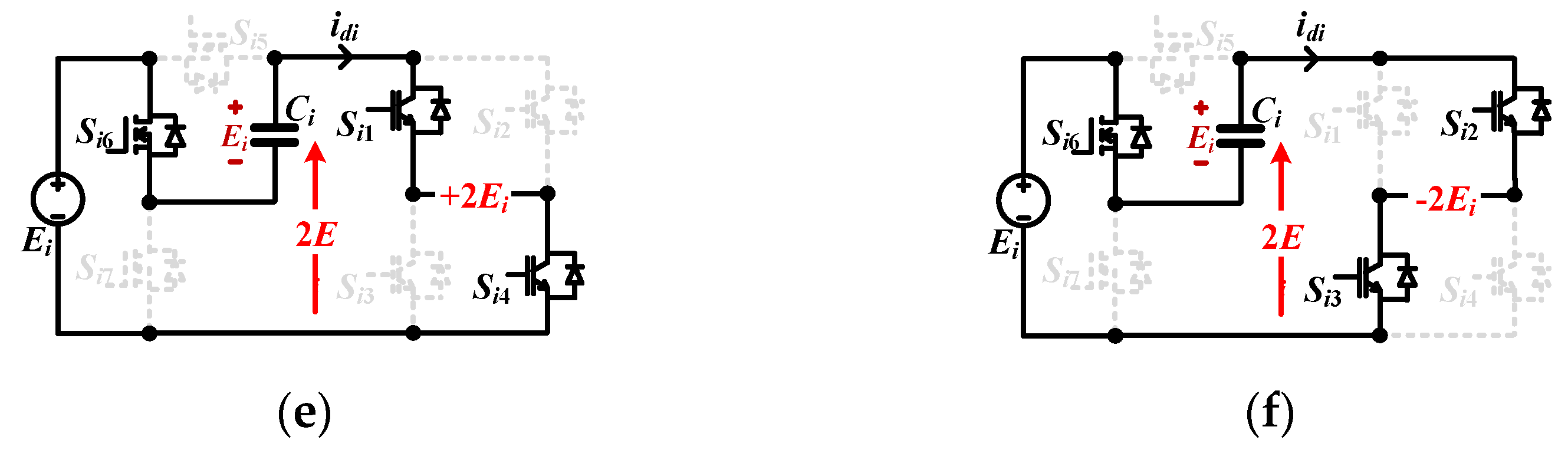
2.2. Operation Principle

In each unit, the SC cell includes switches (Si5, Si6, and Si7) and capacitor Ci, and the H-bridge is composed of switches Si1~Si4. In the SC cell, the switches Si5 and Si7 are turned on/off simultaneously and have a complementary pulse signal with Si6. When Si5 and Si7 are turned on, and Si6 is off, the capacitor Ci is parallelly connected to the dc source, and the dc bus voltage Vbi is equal to Ei. When Si5 and Si7 are turned off, and Si6 is turned on, the capacitor Ci is in series with the dc source. Since Ci was charged to the dc source voltage Ei in the previous state, the dc bus voltage Vbi is equal to 2Ei. It can be concluded that the capacitor is charged when connected in parallel and discharged when connected in series. By converting the capacitor and the dc source in series or in parallel connection, the dc bus has two voltage levels: Ei and 2Ei. With the operation of the H-bridge, a total of five voltage levels is produced for each unit, i.e., 0, ±Ei and ±2Ei. The detailed operation state circuits under resistive load are shown in Figure 2. From the analysis, power switches of different voltage ratings should be selected for the SC cell and H-bridge. The voltage stress of all power switches in the SC cell is Ei, and the voltage stress of switches in the H-bridge is 2Ei.
If the dc sources are independent, and its voltage meets Ei+1 = 3Ei or Ei+1 = 5Ei, the circuit shown in Figure 1 is configured as an asymmetric cascaded switched-capacitor multilevel inverter, from which more voltage levels are produced. However, since the voltage and power rating of each unit is different, each unit needs to be designed separately, and it is difficult to realize the modular design.
If the dc source values are equal to E, the circuit shown in Figure 1 is configured as a symmetrical cascaded switched-capacitor multilevel inverter. The voltage rating of each cell is the same, and its power rating is also the same under appropriate modulation strategy; therefore, modular design is realized, and only a single unit needs to be designed. In the following, we focus on a symmetrical switched-capacitor multilevel inverter cascaded by two units. Five voltage levels of 0, ±E and ±2E are produced by each unit, so the cascaded inverter has a total of 5 × 5 = 25 working status, resulting in nine voltage levels of 0, ±E, ±2E, ±3E and ±4E for the inverter’s output, as shown in Table 1. However, there is only one combination for the output voltage level ±4E, and there are several redundant states for other voltage levels. Therefore, it is important to design the modulation algorithm to select an appropriate redundant state in order that the power between cascaded modules can be balanced automatically and the voltage ripple of the switched capacitor could be minimized.

2.3. Enhanced Reactive Power Capability of the Proposed Circuit

Since the current of the dc bus idi is always positive under resistive load, the switching modes of our proposed circuit and the one in [23] are completely the same. However, there is a significant difference between the two circuits if an inductive load is connected. As shown in Figure 3, when the load is inductive, a phase shift φ between the output voltage and output current of the inverter will lead to a negative idi in the dc bus. Take the first-half period, for example, idi is negative during 0~t2 and positive during t2~t4.
During 0~t2, for our proposed circuit, as shown in Figure 2e, at Mode 5, when the dc bus voltage is 2Ei, the negative idi will charge the capacitor Ci and cause a voltage rise on the capacitor. To the next state, when the dc bus voltage switches to Ei, as shown in Figure 2c, due to the existence of the switch Si5, the capacitor discharges immediately, and its voltage is clamped to the dc source voltage Ei. In contrast, for the proposed circuit in [23], due to the existence of diode in SC cell, whether in Mode 3 or Mode 5, as shown in Figure 4, the negative current idi keeps charging the capacitor. The process continues until the current idi reverses at t2 instant, which results in a continuous rise of the capacitor voltage during 0~t2.
When the output voltage uoi is negative, according to the switching modes of Mode 4 and Mode 6 in Figure 2 and Figure 4, the situation is quite similar. The capacitor voltage of our proposed circuit is maintained around the source voltage Ei, but the capacitor voltage of the inverter in [23] will keep rising until the inverter’s output voltage and current are in the same direction. It is obvious that the reactive power capability in [23] is limited due to its high capacitor voltage, while the proposed circuit in this paper can work properly under a large inductive load.

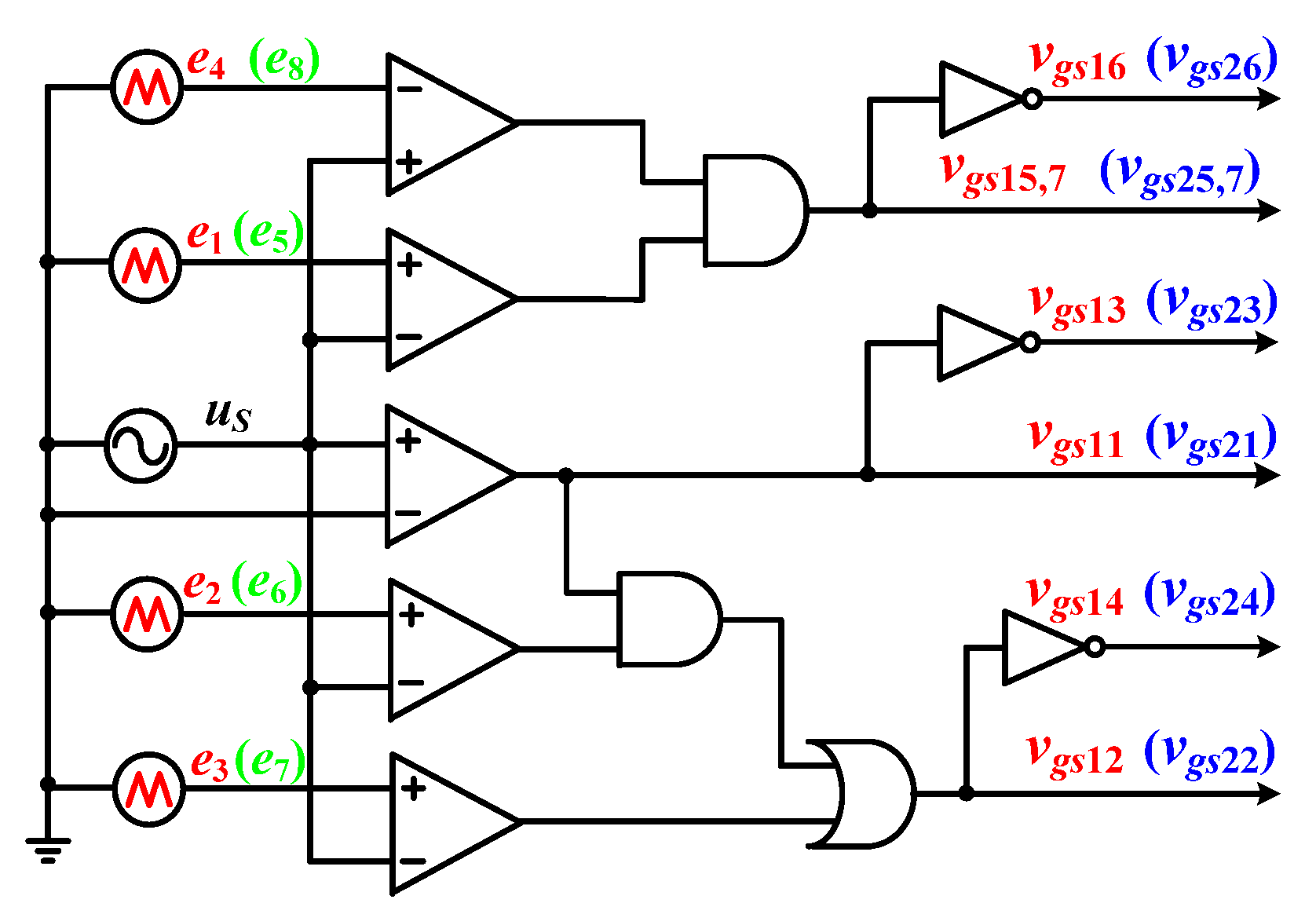
3. Modulation Strategy

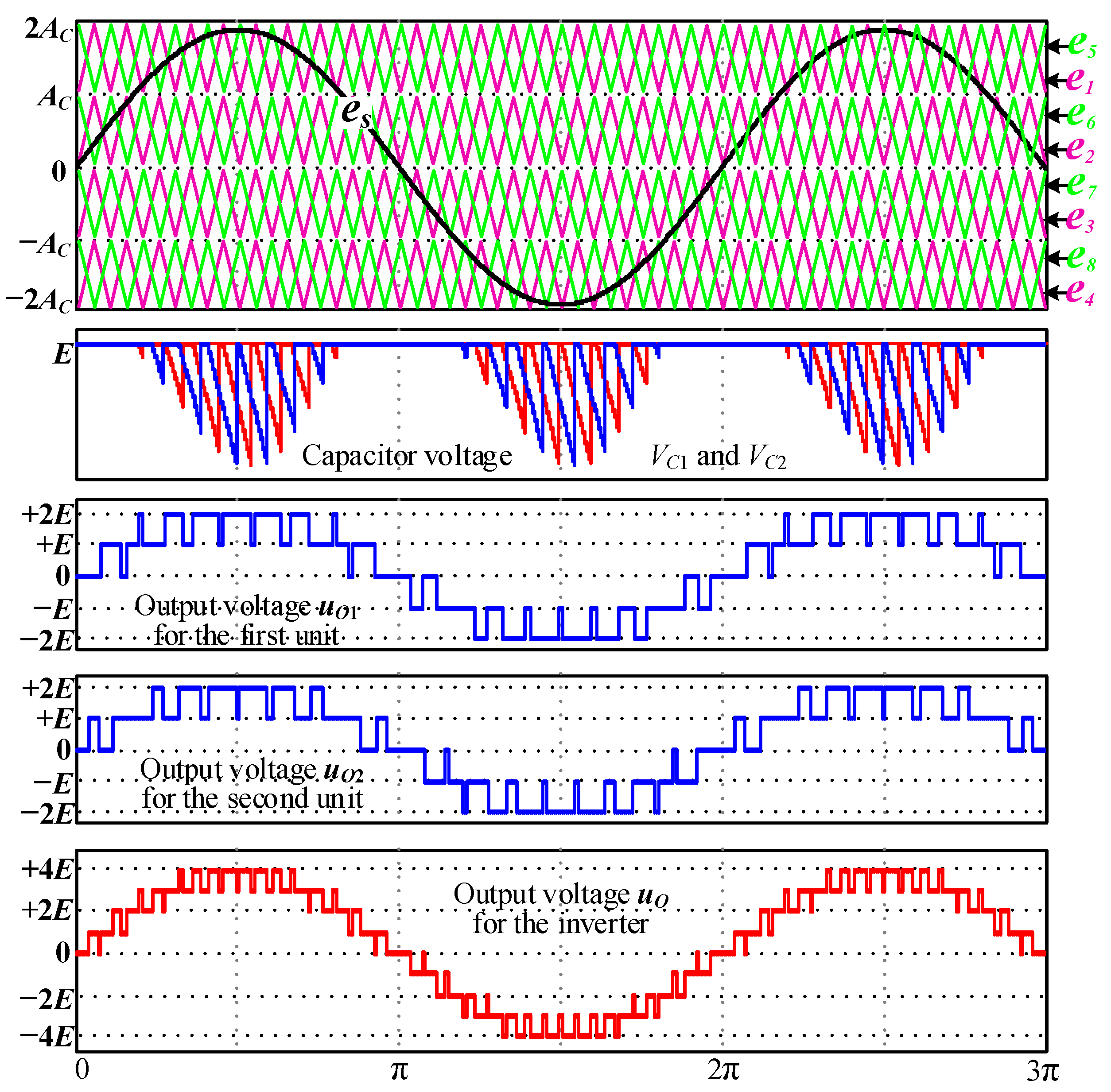
3.1. Hybrid Pulse Width Modulation

LS-PWM and PS-PWM are two of the most commonly used modulation strategies for a conventional multilevel inverter. As discussed above, five-level voltage is produced by each unit in the proposed cascaded multilevel inverter, which can be modulated using LS-PWM with four carriers. With LS-PWM, in addition, a high-quality output waveform of an inverter is achieved by charging and discharging the capacitor of SC cell alternatively in high frequency, the voltage of the capacitor is automatically balanced and the voltage ripple of the capacitor could be minimized. As for symmetrical cascaded units, PS-PWM is a good choice when using which power between cascaded units is automatically balanced. Therefore, by combining PS-PWM and LS-PWM, a hybrid pulse width modulation for a nine-level inverter is provided in Figure 5. With this hybrid modulation, power balancing between cascaded units and the capacitor voltage ripple minimization can both be achieved.
In Figure 5, es is the modulating signal with amplitude Aref, and e1~e8 are carriers. The level-shifted carriers e1 ~ e4 have the same phase, which is compared with the modulating signal to generate switching control signals for the first cascaded unit. Similarly, the level-shifted carriers e5~e8, whose phase is opposite to e1~e4, are compared with the modulating signal for generating switching control signals for the second cascaded unit. It can be seen from Figure 5, five voltage levels of 0, ±E and ±2E are produced for the output (uo1 and uo2) in each unit, and a nine-level output voltage (uo) of 0, ±E, ±2E, ±3E and ±4E is obtained by cascading two units. It was noted that for each unit, when the output voltage is switching between +E and +2E, the capacitor operates in charging and discharging mode alternately in high frequency. Therefore, the capacitor voltage can be balanced to dc input voltage automatically, and the voltage ripple of the capacitor can be minimized.
The modulation index is defined as
M = A r e f 2 A c
where Ac is the peak-to-peak amplitude of the carriers.
The operating status of each switch in the cascaded inverter is given in Table 2, where “↓” and “↑” represent capacitor discharging and charging, respectively.
According to Table 2 and Figure 5, the modulation logic of switching control signals in the first cascaded unit can be summarized as follows. When es > 0, the control signal of S11 satisfies vgs11 = 1, which is complementary to control signal of S13; when 0 < es < e2 or es < e3, the control signal of S12 satisfies vgs12 = 1, which is complementary to control signal of S14; when e4 < es < e1, the control signals of S15 and S17 satisfy vgs15 = vgs17 = 1, which is complementary to the control signal of S16. Similarly, the modulation logic of switching control signals in the second cascaded unit is shown as follows: when es > 0, vgs21 = 1; when 0 < es < e6 or es < e7, vgs22 = 1; when e8 < es < e5, vgs25 = 1. Thus, the logic modulating circuit of hybrid pulse width modulation is shown in Figure 6.
The hybrid pulse width modulation strategy described above can be easily extended to a symmetrical cascaded multilevel inverter cascaded by n units. Switching control signals in each unit is still generated from the modulating circuit in Figure 6, and the phase shift between different carrier sets for cascaded units should be set to (360/n) °.

3.2. Harmonic Analysis of Output Voltage

Assuming the capacitor voltage is equal to E, the Fourier transform of the inverter output voltage can be expressed as
u o = E [ 4 M cos ( ω 0 t ) + i = 1 8 m = 1 + n = + A m n i cos ( n ω 0 t + m ω c t + m α i ) ]
where ω 0 and ω c are the frequency of modulating signal and carriers, respectively. Amni is the amplitude of harmonics caused by the i-th carrier centering at the frequency of n ω 0 + m ω c , and αi is the phase angle of the i-th carrier.
In addition, Amni is equal to 0 when m + n is an even number [25]. In the proposed hybrid pulse width modulation, the phase difference between two sets of carrier signals is 180°; thus, the harmonics generated from two cascaded units cancel each other when m is an odd number, and the harmonics only need to be considered when m is an even number.

3.3. Power Balance

As discussed above, in the hybrid pulse width modulation, a single modulating signal and two sets of carriers of opposite phases are utilized. From (2), the fundamental component of the output voltage is independent of the carrier; thus, the fundamental power in two cascaded units is equal.
Considering the harmonic component of the multilevel output voltage is low, the power dissipated by the harmonic current can be neglected. Therefore, the output power of each unit approaches, and power balancing is realized automatically.

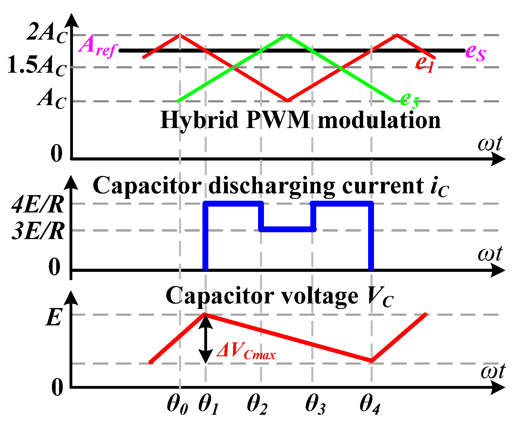
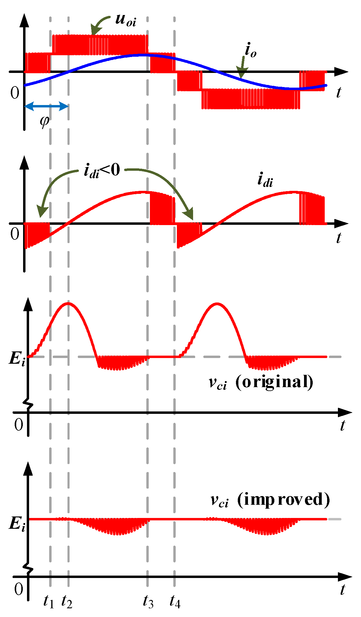
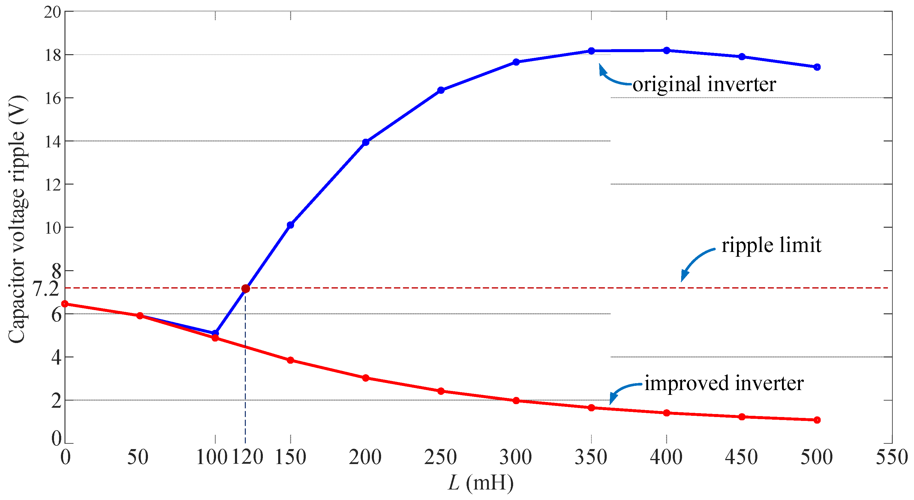
4. Capacitor Voltage Ripples

With the hybrid pulse width modulation, the capacitor in the SC cell operates alternately in series and in parallel with the dc voltage source. The capacitor voltage is clamped to dc voltage E whenever it is connected in parallel with the source, so the voltage ripple of the capacitor is proportional to the integral of discharging current and is inversely proportional to its capacitance.
The integral of discharging current takes the maximum value when the modulating signal es reaches its peak Aref. The discharging current and capacitor voltage are given in Figure 7 when a pure resistive load R is connected.
The maximum capacitor voltage ripple can be expressed as
Δ V C m a x = E R C [ θ 1 θ 2 4 d ( ω t ) + θ 2 θ 3 3 d ( ω t ) + θ 3 θ 4 4 d ( ω t ) ]
Based on a similar triangle theory, it can be further expressed as
Δ V C m a x = ( 5 A r e f / A C 6 ) R C f C = ( 10 M 6 ) E R C f C
where fC is the frequency of carriers e1~e8.
The capacitor satisfies
C > 10 M 6 α R f C
where α = ∆VCmax/E represents the allowable ripple voltage across the capacitors, and it is normally set around 10%.

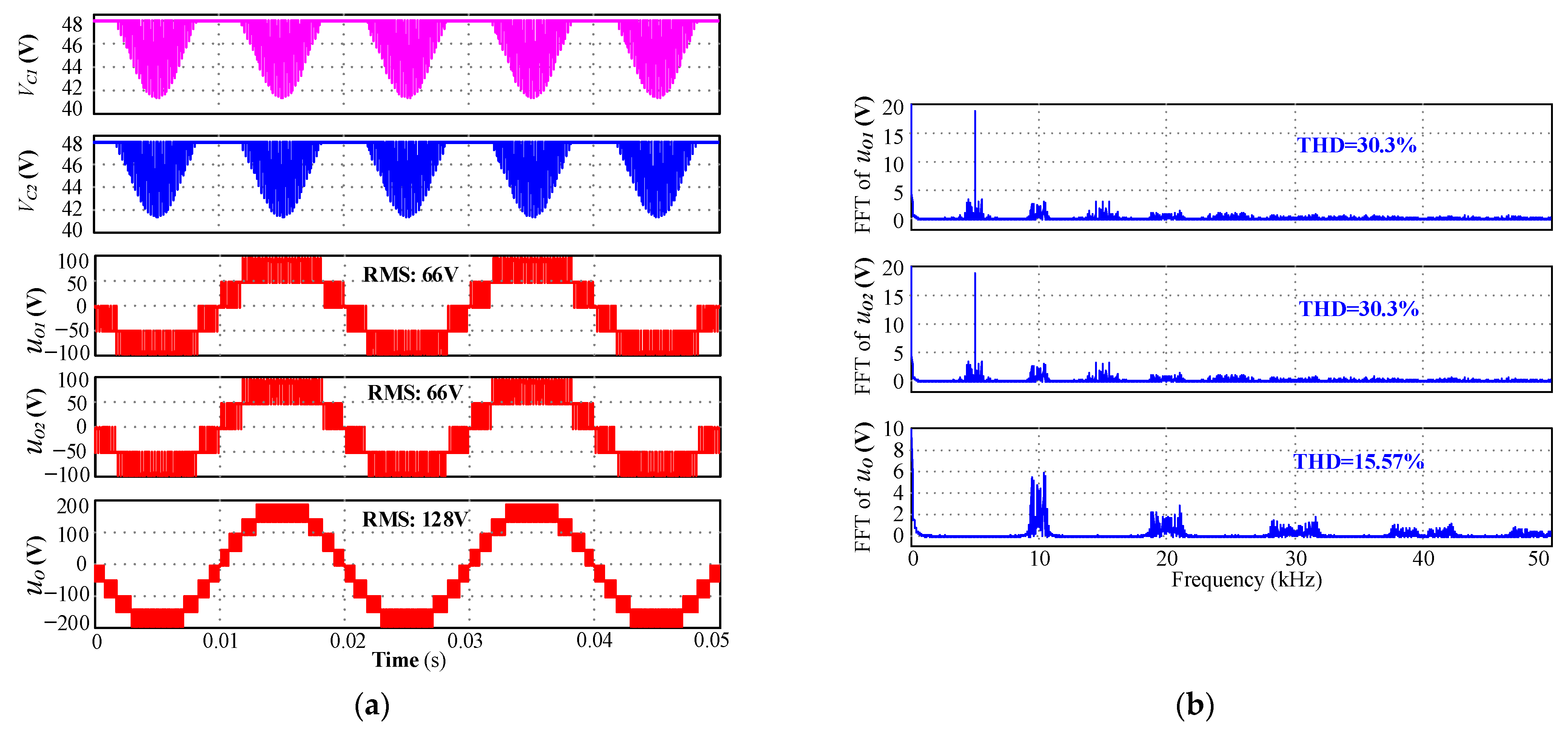
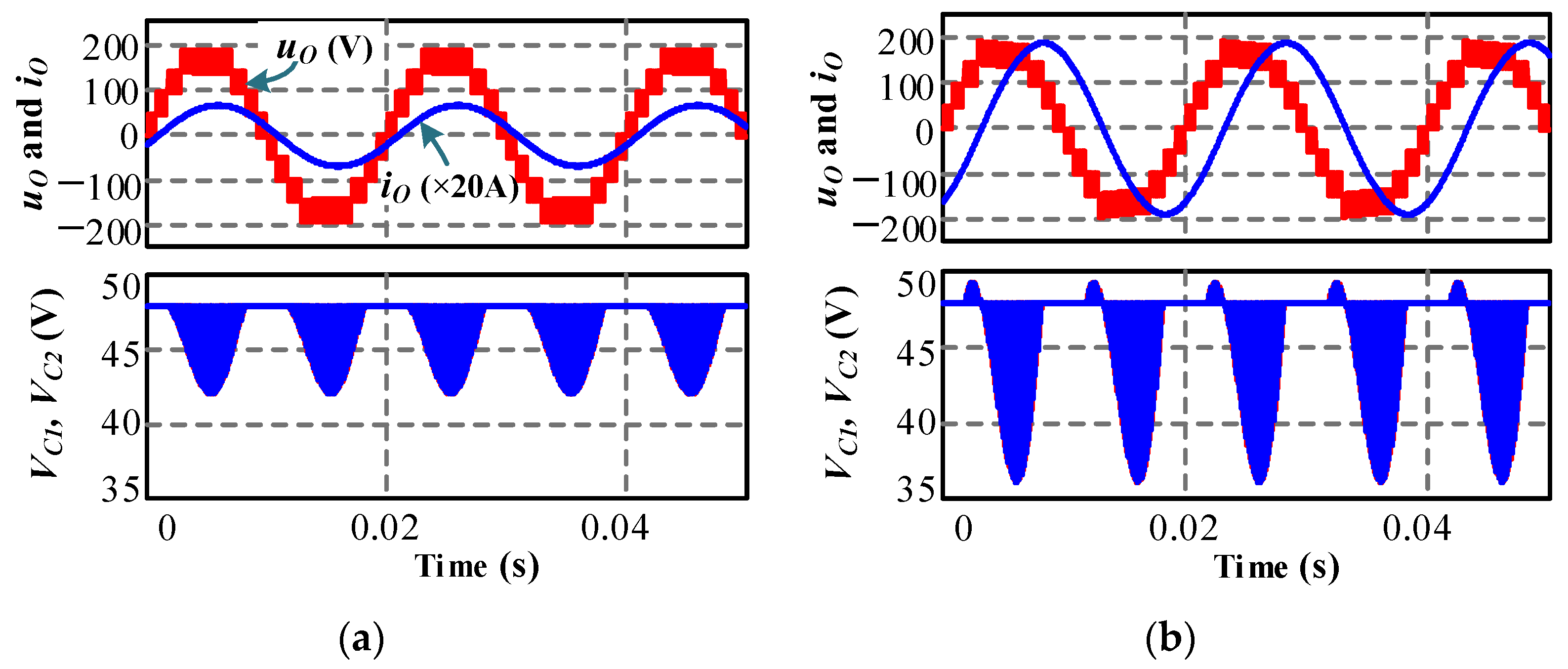
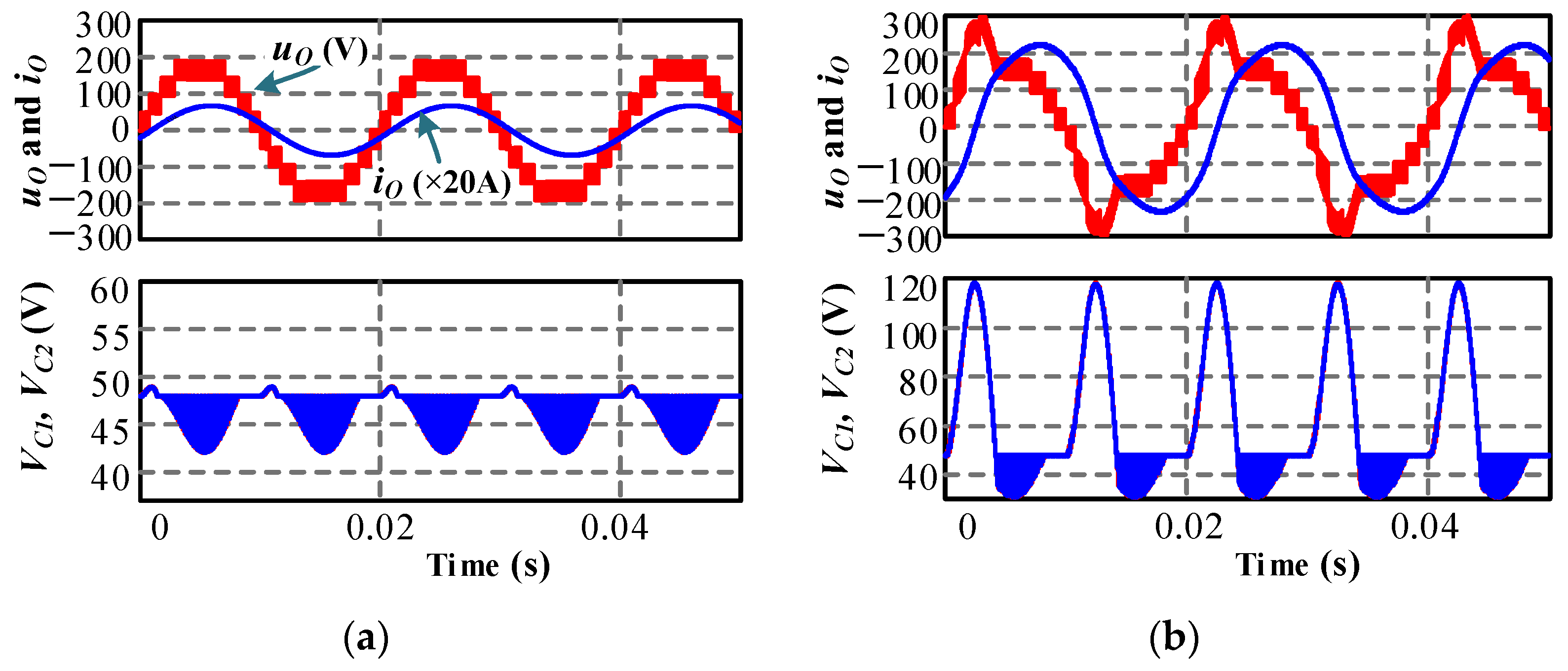
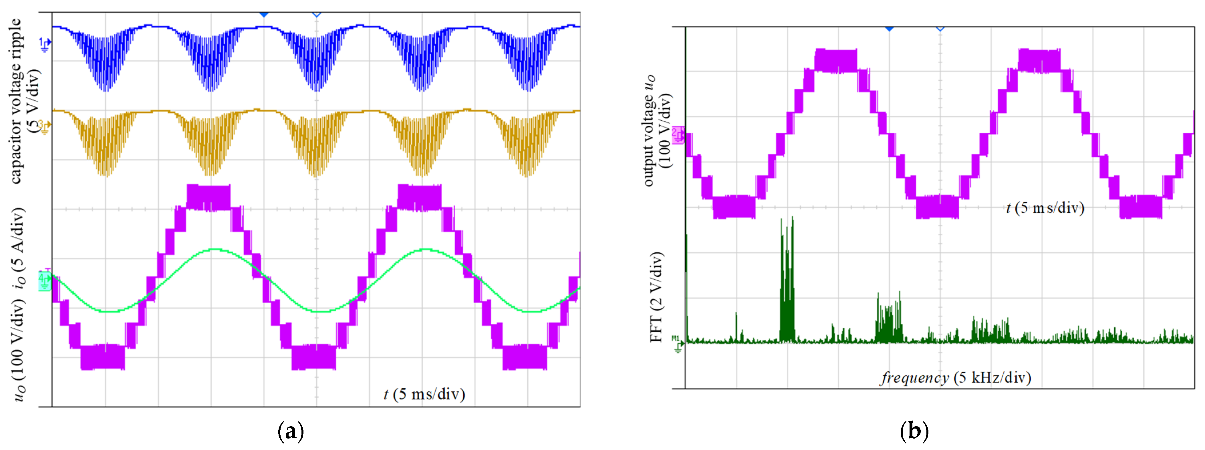
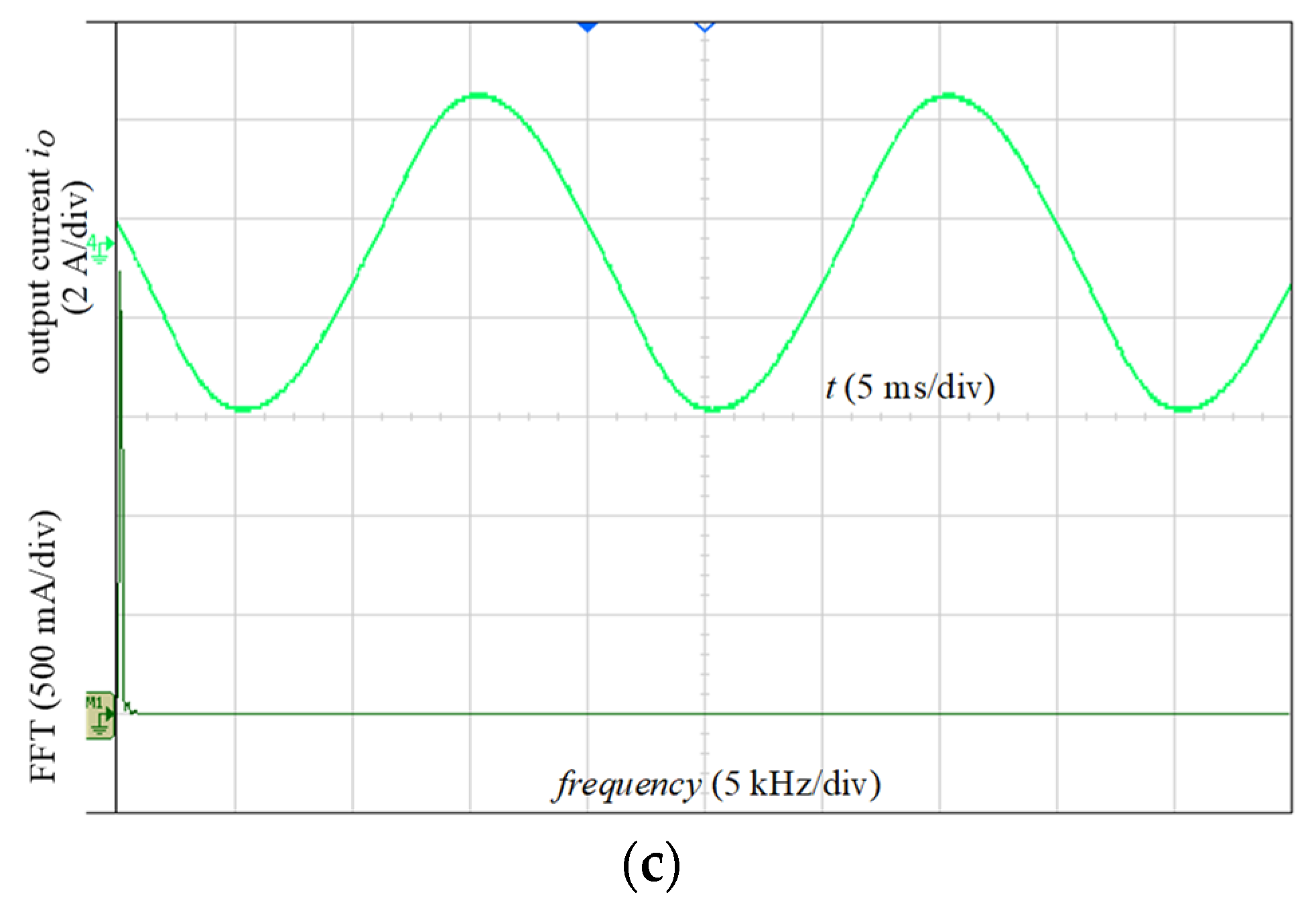
5. Simulation Verification

In order to verify the effectiveness of the proposed symmetrical switched-capacitor multilevel inverter and its hybrid pulse width modulation, a simulation model was built in PSIM. The simulation parameters are listed in Table 3.
Figure 8 shows the simulation results under the 50 Ω load condition. As shown in Figure 8a, a five-level output voltage is produced by each unit, and a nine-level output voltage is generated by cascading two units. Since the RMS value of output voltage in each unit is measured the same as 66 V, it can be deduced that the power of each cascaded unit is equal, and the power between two cascaded units is automatically balanced. Moreover, the capacitor voltage is balanced to the dc input voltage by using hybrid PWM. From the FFT analysis result in Figure 8b, the voltage harmonics of each unit are distributed near the carrier frequency (5 kHz) and its multiples (10 kHz, 15 kHz, …), while the harmonics of the total output voltage are located near even multiples of the carrier frequency (10 kHz, 20 kHz, …), showing that the equivalent switching frequency after cascading is increased to twice the carrier frequency.
Figure 9 shows the simulation waveforms under inductive load. It can be seen that the capacitor keeps the voltage around the dc input voltage due to the clamping of Si5, and the inverter works properly even when the reactive power demand is large. For comparison, the cascaded inverter using a diode in the SC cell [23] is also simulated, and the simulation results are shown in Figure 10. It can be seen that the capacitor voltage is far beyond the dc input voltage because the diode prevents the current flow, and the reversing current keeps charging the capacitor in the SC cell. The output voltage waveform is heavily distorted, as shown in Figure 10b, and the overvoltage of capacitors might cause some safety issues. Thus, the optimized topology in this paper, by simplifying replacing the diode with MOSFET, improves not only the performance of the inverter under inductive load but also the system’s reliability.
In order to compare the reactive power capability of the proposed circuit and the inverter in [23], the capacitor voltage ripple with different inductive loads is depicted in Figure 11. Assuming that the limitation of capacitor voltage ripple is 15% Ei, i.e., ∆VCmax = 7.2 V, with the inverter in [23], the ripple will reach the limitation when the inductance increases to 120 mH and the power factor of the inverter is about 0.798. With the proposed circuit in this paper, as shown in Figure 11, the voltage ripple will never exceed the limitation even with a large inductance.
Compared to the power factor of [0.798,1] in [23], the power factor is extended to [0,1] for our proposed circuit, which has demonstrated an enhanced reactive power capability.
On the other side, the proposed circuit has a smaller voltage ripple on the capacitor under the same inductive load, which means that the capacitance required can be reduced. Therefore, an electrolytic capacitor could be replaced by a film capacitor featuring a long lifetime and high reliability.

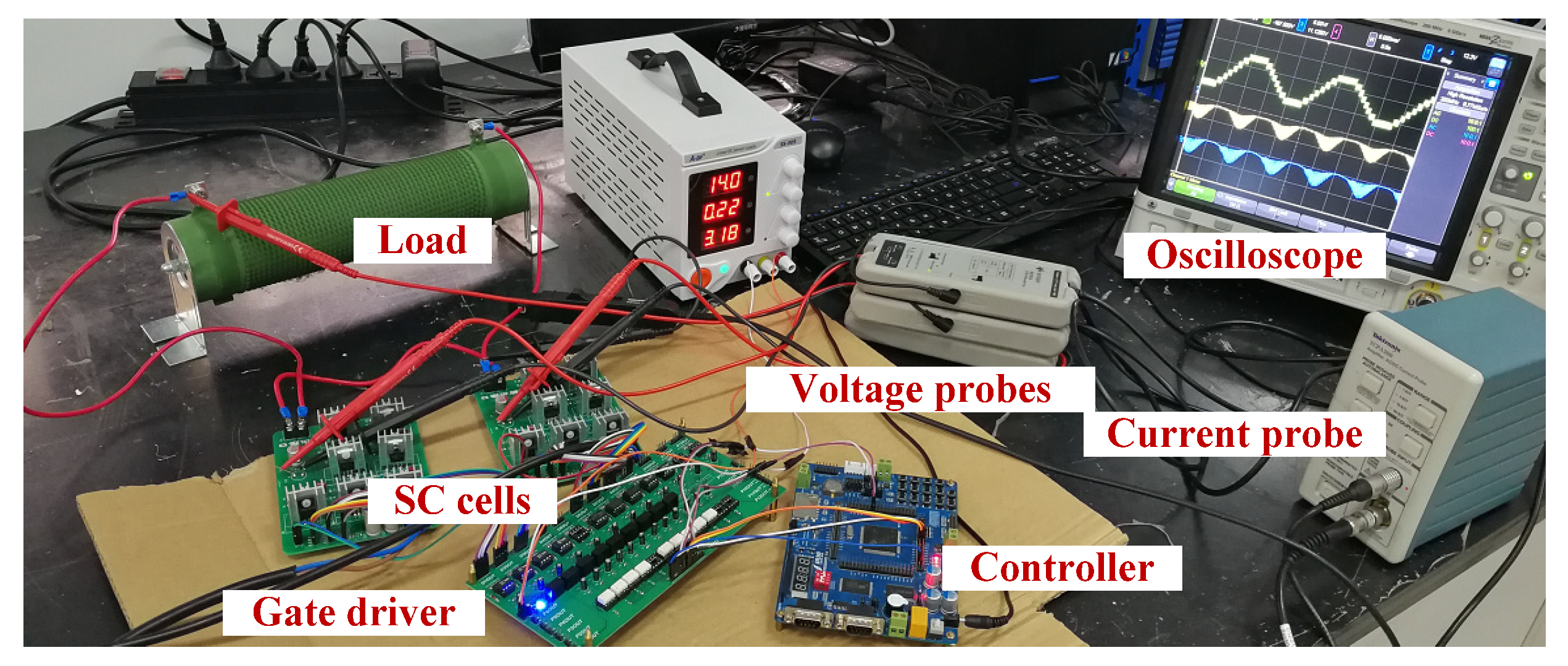
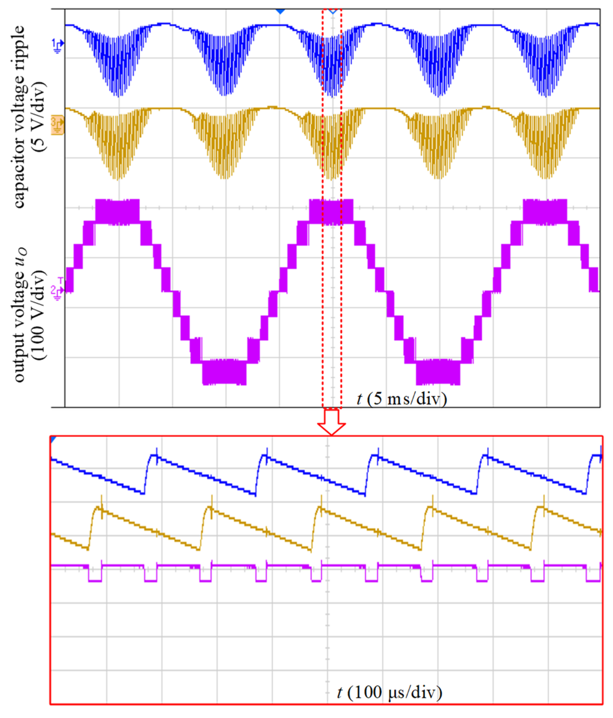
6. Experimental Verification

A prototype is also built. The parameters are listed in Table 3, and the experiment bench is shown in Figure 12. In the experiment, the hybrid modulation strategy illustrated in Figure 3; Figure 4 is realized using a DSP microcontroller. The generated control signals are sent to power switches through the optocoupler.
Figure 13 shows the experimental waveforms for a resistive load. The proposed switched-capacitor multilevel inverter cascaded by two units can generate a nine-level output voltage with a step voltage of 48 V. The RMS value of output voltage is measured as 125.84 V, which is close to the simulation value (126 V). By using hybrid PWM modulation, the capacitors are charged and discharged alternately, obtaining a high-quality output voltage waveform with a small capacitor (100 μF). In addition, the voltage of each capacitor is automatically balanced, and their voltage ripple is almost the same, which means that the transferred power in cascaded units is balanced automatically.
Figure 14 shows the experimental waveforms for an inductive load. In Figure 14a, the waveforms of capacitor voltage, output voltage and output current are shown. It shows that the capacitor voltage balancing and power balancing between cascaded units are realized. The FFT analysis of output voltage is shown in Figure 14b. It is shown that the harmonics are mainly distributed around even multiples of the carrier frequency, i.e., 10 kHz, 20 kHz and 30 kHz, which coincides with theoretical analysis and simulation results. The FFT analysis of output current is shown in Figure 14c, which indicates that the output current is a pure sine wave without containing any harmonics.
The relationship between the system efficiency and output power is achieved in Figure 15 by adjusting the value of the resistive load. The results show that the efficiency of the inverter is larger than 92% when the power ranges from 24 W to 222 W. Especially, the efficiency is larger than 97% when the output power is larger than 50 W. It is obvious that the inverter has a high efficiency over a wide load range.

7. Conclusions

In this paper, an optimized symmetrical switched-capacitor multilevel inverter was proposed, and a hybrid pulse width modulation strategy combining LS-PWM and PS-PWM was applied. The theoretical analysis, simulation results and experimental results are provided. Compared to the inverter in [23], the proposed multilevel inverter has the following advantages:
(1)
With LS-PWM, a five-level output voltage is produced for each cascaded unit, and the capacitor voltage can be balanced to the dc input voltage automatically. The capacitor keeps charging and discharging alternately in high frequency so that only a small capacitor is needed to minimize the capacitor voltage ripple;
(2)
With PS-PWM, power balancing between cascaded units is realized automatically. The equivalent switching frequency of the cascaded inverter is increased to twice the carrier frequency; therefore, the harmonics of the output voltage is located near even multiples of the carrier frequency;
(3)
It has superior reactive power capability and reliability.

Author Contributions

Conceptualization, Y.Y.; methodology, Y.Y. and L.C.; software, J.L.; validation, S.C.; formal analysis, J.L.; investigation, L.C.; data curation, S.C.; writing— J.L.; writing—review and editing, L.C.; supervision, Y.Y.; funding acquisition, L.C. All authors have read and agreed to the published version of the manuscript.

Funding

This research was funded by National Natural Science Foundation of China grant number 52007040.

Institutional Review Board Statement

Not applicable.

Informed Consent Statement

Not applicable.

Data Availability Statement

The data presented in this study are available on request from the corresponding author.

Conflicts of Interest

The authors declare no conflict of interest.

References

  1. Franquelo, L.G.; Rodriguez, J.; Leon, J.I.; Kouro, S.; Portillo, R.; Parts, M.A.M. The age of multilevel converters arrives. IEEE Ind. Electron. Mag. 2008, 2, 28–39. [Google Scholar] [CrossRef] [Green Version]
  2. Li, Z.; Wang, P.; Li, Y.; Gao, F. A novel single-phase five-level inverter with coupled inductors. IEEE Trans. Power Electron. 2012, 27, 2716–2725. [Google Scholar] [CrossRef]
  3. Ben Smida, M.; Ben Ammar, F. Modeling and DBC-PSC-PWM control of a three-phase flying-capacitor stacked multilevel voltage source inverter. IEEE Trans. Ind. Electron. 2010, 57, 2231–2239. [Google Scholar] [CrossRef]
  4. Rodriguez, J.; Bernet, S.; Steimer, P.K.; Lizama, I.E. A survey on neutral-point-clamped inverters. IEEE Trans. Ind. Electron. 2010, 57, 2219–2230. [Google Scholar] [CrossRef]
  5. Lara, J.; Masisi, L.; Hernandez, C.; Arjona, M.A.; Chandra, A. Novel single-phase grid-tied NPC five-level converter with an inherent DC-link voltage balancing strategy for power quality improvement. Energies 2021, 14, 2644. [Google Scholar] [CrossRef]
  6. McGrath, B.P.; Holmes, D.G.; Kong, W.Y. A decentralized controller architecture for a cascaded H-bridge multilevel converter. IEEE Trans. Ind. Electron. 2014, 61, 1169–1178. [Google Scholar] [CrossRef]
  7. Sepahvand, H.; Liao, J.; Ferdowsi, M.; Corzine, K.A. Capacitor voltage regulation in single-DC-source cascaded H-bridge multilevel converters using phase-shift modulation. IEEE Trans. Ind. Electron. 2013, 60, 3619–3626. [Google Scholar] [CrossRef]
  8. Marquardt, R. Modular multilevel converters: State of the art and future progress. IEEE Power Electron. Mag. 2018, 5, 24–31. [Google Scholar] [CrossRef]
  9. Gohari, A.; Afjei, E.S.; Torkaman, H. Novel symmetric modular hybrid multilevel inverter with reduced number of semiconductors and low-voltage stress across switches. IEEE J. Emerg. Sel. Top. Power Electron. 2020, 8, 4297–4305. [Google Scholar] [CrossRef]
  10. Tang, Y.; Xie, S.; Zhang, C.; Xu, Z. Improved Z-source inverter with reduced Z-source capacitor voltage stress and soft-start capability. IEEE Trans. Power Electron. 2009, 24, 409–415. [Google Scholar] [CrossRef]
  11. Meraj, M.; Rahman, S.; Iqbal, A.; Ben-Brahim, L.; Abu-Rub, H.A. Novel level-shifted PWM technique for equal power sharing among quasi-Z-source modules in cascaded multilevel inverter. IEEE Trans. Power Electron. 2021, 36, 4766–4777. [Google Scholar] [CrossRef]
  12. Ravindranath, A.; Mishra, S.K.; Joshi, A. Analysis and PWM control of switched boost inverter. IEEE Trans. Ind. Electron. 2013, 60, 5593–5602. [Google Scholar] [CrossRef]
  13. Kumar, A.; Wang, Y.; Raghuram, M.; Pilli, N.K.; Singh, S.K.; Pan, X.; Gang, X. A generalized switched inductor cell modular multilevel inverter. IEEE Trans. Ind. Appl. 2020, 56, 507–518. [Google Scholar] [CrossRef]
  14. Mak, O.C.; Ioinovici, A. Switched-capacitor inverter with high power density and enhanced regulation capability. IEEE Trans. Circuits Syst. I Fundam. Theory Appl. 1998, 45, 336–347. [Google Scholar]
  15. Xun, Z.; Ding, H.; He, Z. A novel switched-capacitor inverter with reduced capacitance and balanced neutral-point voltage. Electronics 2021, 10, 947. [Google Scholar] [CrossRef]
  16. Qiang, H.; Wu, Z.; Xu, T.; Kong, P.; Mao, S.; Zheng, J. Boost voltage single phase full bridge inverter with no voltage drop based on switched capacitor. Energies 2021, 14, 3466. [Google Scholar] [CrossRef]
  17. Hinago, Y.; Koizumi, H. A single-phase multilevel inverter using switched series/parallel DC voltage sources. IEEE Trans. Ind. Electron. 2010, 57, 2634–2650. [Google Scholar] [CrossRef]
  18. Hinago, Y.; Koizumi, H. A switched-capacitor inverter using series/parallel conversion with inductive load. IEEE Trans. Ind. Electron. 2012, 59, 878–887. [Google Scholar] [CrossRef]
  19. Ye, Y.; Cheng, K.W.E.; Liu, J.; Ding, K. A step-up switched-capacitor multilevel inverter with self-voltage balancing. IEEE Trans. Ind. Electron. 2014, 61, 6672–6680. [Google Scholar] [CrossRef]
  20. Peng, W.; Ni, Q.; Qiu, X.; Ye, Y. Seven-level inverter with self-balanced switched-capacitor and its cascaded extension. IEEE Trans. Power Electron. 2019, 34, 11889–11896. [Google Scholar] [CrossRef]
  21. Sun, X.; Wang, B.; Zhou, Y.; Wang, W.; Du, H.; Lu, Z. A single DC source cascaded seven-level inverter integrating switched-capacitor techniques. IEEE Trans. Ind. Electron. 2016, 63, 7184–7194. [Google Scholar] [CrossRef]
  22. Ye, Y.; Lin, M. Single source step-up multilevel inverter based on switched capacitor. Proc. CSEE 2020, 40, 5636–5644. [Google Scholar]
  23. Liu, J.; Cheng, K.W.E.; Ye, Y. A cascaded multilevel inverter based on switched-capacitor for high-frequency ac power distribution system. IEEE Trans. Power Electron. 2014, 29, 4219–4230. [Google Scholar] [CrossRef]
  24. Babaei, E.; Gowgani, S.S. Hybrid multilevel inverter using switched capacitor units. IEEE Trans. Ind. Electron. 2014, 61, 4614–4621. [Google Scholar] [CrossRef]
  25. Rodriguez, J.; Lai, J.-S.; Peng, F.Z. Multilevel inverters: A survey of topologies, controls, and applications. IEEE Trans. Ind. Electron. 2002, 49, 724–738. [Google Scholar] [CrossRef] [Green Version]
Figure 1. Cascaded switched-capacitor multilevel converter.
Energies 14 07643 g001
Figure 2. Switching modes of an optimized cascaded unit. (a) Mode 1, (b) Mode 2, (c) Mode 3, (d) Mode 4, (e) Mode 5, (f) Mode 6.
Energies 14 07643 g002aEnergies 14 07643 g002b
Figure 3. Operation waveforms under inductive load.
Energies 14 07643 g003
Figure 4. Switching modes of the inverter in [23] under inductive load. (a) Mode 1, (b) Mode 2, (c) Mode 3, (d) Mode 4, (e) Mode 5, (f) Mode 6.
Energies 14 07643 g004
Figure 5. Modulation principle of hybrid PWM.
Energies 14 07643 g005
Figure 6. Modulating logic circuit of hybrid PWM.
Energies 14 07643 g006
Figure 7. The maximum capacitor voltage ripple.
Energies 14 07643 g007
Figure 8. Simulation waveforms for a resistive load: (a) Output voltage and capacitor voltage ripple; (b) FFT analysis result of output voltage.
Energies 14 07643 g008
Figure 9. Simulation waveforms for the optimized inverter with inductive loads: (a) 50 Ω-50 mH; (b) 10 Ω-50 mH.
Energies 14 07643 g009
Figure 10. Simulation waveforms for the original inverter with inductive loads: (a) 50 Ω-50 mH; (b) 10 Ω-50 mH.
Energies 14 07643 g010
Figure 11. Capacitor voltage ripple versus load inductance (R = 50 Ω).
Energies 14 07643 g011
Figure 12. Experiment bench.
Energies 14 07643 g012
Figure 13. Experimental waveforms for a resistive load.
Energies 14 07643 g013
Figure 14. Experimental waveforms for an inductive load: (a) Waveforms of output voltage, output current, and capacitor voltage; (b) FFT analysis of output voltage; (c) FFT analysis of output current.
Energies 14 07643 g014aEnergies 14 07643 g014b
Figure 15. Efficiency versus output power.
Energies 14 07643 g015
Table 1. Working status of the cascaded inverter.
NumberuO1uO2uO
1+2E+2E+4E
2+2E+E+3E
3+E+2E
4+E+E+2E
50+2E
6+2E0
7+E0+E
80+E
9+2EE
10E+2E
11+2E−2E0
12+EE
1300
14E+E
15−2E+2E
16−2E+EE
17+E−2E
180E
19E0
200−2E−2E
21−2E0
22EE
23−2EE−3E
24E−2E
25−2E−2E−4E
Table 2. Operating status of each switch.
StatusCapacitor StatusOutput Level
Si1Si2Si3Si4Si5Si6Si7
1001010+2E
1001101+E
11001010
00111010
0110101E
0110010−2E
Table 3. Parameters of the cascaded multilevel inverter.
ParametersSimulationExperiment
E48 V48 V
M0.950.95
f0/fC50 Hz/5 kHz50 Hz/5 kHz
C1, C2100 μF100 μF
S15~17, S25~27Ideal switchIRFI4410Z
S11~14, S21~24Ideal switchIRF640
Load50 Ω/50 Ω-50 mH/10 Ω-50 mH50 Ω/50 Ω-53 mH
Publisher’s Note: MDPI stays neutral with regard to jurisdictional claims in published maps and institutional affiliations.

