Article

Modeling, Analysis, and Control Design of a Single-Stage Boost Inverter

1
Department of Engineering and Technology, Southeast Missouri State University, Cape Girardeau, MO 63701, USA
2
Department of Electrical & Biomedical Engineering, University of Nevada, Reno, NV 89557, USA
3
Department of Electrical & Computer Engineering, Missouri University of Science and Technology, Rolla, MO 65409, USA
*
Author to whom correspondence should be addressed.
Energies 2021, 14(14), 4098; https://doi.org/10.3390/en14144098
Submission received: 8 June 2021 / Revised: 30 June 2021 / Accepted: 1 July 2021 / Published: 7 July 2021
(This article belongs to the Special Issue Power Converters Design, Control and Applications)

Abstract

:
A single-phase, single-stage, differential boost inverter comprises two independently-controlled boost DC-DC converters, with the load connected between their outputs. The net voltage on the load is sinusoidal and has a controllable frequency and magnitude that is larger than that of the DC source. The present work first derives steady-state and small-signal models of the inverter with parasitic elements. The results obtained from the line-to-output transfer function, control-to-output transfer function, open-loop input impedance, and open-loop output impedance models are compared with that of the ones obtained from the experimental testbed. Using the new models, a voltage mode controller is designed in the synchronous reference frame. The regulator design is explored through the use of an example. The results are verified against the small-signal model, then PLECS simulations, and finally a laboratory experiment. The results indicate excellent agreement between the model and experiment during transients in voltage reference, input source voltage, and output load. A sensitivity analysis is performed based on the inverter model considering the parameter variation. Finally, loss and efficiency estimations are provided in this work.

1. Introduction

Traditional full-bridge inverters are buck type, meaning that the generated output voltage magnitude is lower than that of the DC input voltage. To generate an output voltage that is larger in magnitude than the input voltage, an additional boost stage is needed. With the two-stage configuration, the input DC signal is first stepped up using a boost converter and then passed through a buck-type full-bridge inverter. The drawbacks of the two stage configuration are discussed in [1]. Additionally, the efficiency and footprint of the two stage system are not attractive. Considering the complexity of this multistage design, a simple single-stage boost inverter was first proposed by Cáceres and Barbi [2]. The proposed system was designed for a single-phase system. Using this method only four electronic switches are engaged, in contrast to the six switches that are used in a traditional two-stage inverter. Xue et al. in [3] reported that the inverter presented by Cáceres in [2] is one of the topologies of single-phase inverters for small distributed power generators. It is reported that this particular inverter topology has the capability to operate both as a stand-alone and grid-connected power supply unit. The suggested applications of this type of inverter can be found in solar photovoltaic units, wind turbine systems, and fuel cell inverters [4,5,6].
Several single-phase, single-stage, current-source-based inverters (CSI) are discussed in [7]. In [1], a modified modulation technique and a double-tuned resonant filter has been proposed to improve the harmonic response on the DC side with relatively small inductance. The literature review in [7] discusses some challenges associated with the basic boost inverter structure. For improved operation, a new type of single-stage boost inverter is proposed in the same literature. However, the proposed model uses a series capacitor at the output to filter out the DC component which carries the fundamental current. In addition, the inverter fails to operate if a capacitive load is connected. The switched-capacitor differential boost inverter (SCDBI) discussed in [8,9] implemented a gain linearization strategy with the use of unipolar modulation (3L-PWM) resulting in a significant reduction of total harmonic distortion (THD) of the output voltage. However, the SCDBI inverter uses four additional switches. Although several single-stage inverter topologies exist in the literature [10,11,12], the one discussed in [2] has the simplest configuration.
Considering the simplicity of its operation, the inverter in [2] is discussed in this work. The inverter consists of two DC-DC synchronous boost converters. These converters are controlled independently. The inverter has four MOSFET/IGBT switches (two for each boost configuration), two inductors, and two capacitors. Identical inductors and capacitors are used for both converters. The load is connected differentially across the two output capacitors. With this configuration, the inverter was analyzed in [13] considering four different switching states. In [14], only two switching modes are considered. However, both analysis techniques excluded component parasitic from the discussion. The latter technique assumed one of the converters to be a fixed DC source which reduced the system dynamics to only one converter. The models describing the control-to-output relationship in [2,15] do not include component parasitic. The derived transfer functions contain higher-order polynomials in the denominator, which complicates controller design. In addition to that, the transfer functions for the open-loop input impedance and output impedance are not well explained in the previous work. In this work, the boost inverter operation is discussed using two operating modes. Converter dynamics from both the boost operations are considered in deriving the control-to-output transfer function. The mathematical modeling includes the component parasitic resulting in a more accurate representation of the system dynamics. Furthermore, the open-loop input and output impedance are derived and analyzed.
The primary control objective of a single-stage boost inverter is to regulate the individual converters in a way so as to generate a sinusoidal waveform with the nominal operating frequency added to a DC offset. The AC waveforms are 180° out of phase with respect to each other. The differential connection at the load terminals cancels out the DC offsets from both the converters, leaving a sinusoidal signal. The two algorithms that are commonly used in controlling boost inverters are the sliding mode controller and the current mode controller [4,16,17,18,19,20,21,22]. The major issues involving the sliding mode controller are variable switching frequency and complex operating theory [2,23]. The current-controlled theory presented in [18,24] overcomes these issues. However, linearization of the current-controlled model is difficult once control variables and states are considered. Both sliding mode and current-controlled mode controllers require the use of multiple voltage and current sensors.
To overcome these issues, a simple voltage-mode controller for operating the boost inverter is proposed in this work. The proposed controller requires only two voltage measurements. This results in a simpler controller algorithm that eliminates the need for an extra inner loop for current control. This in turn eliminates the need for current sensors and results in a cost-effective design. The voltage mode control of such an inverter was proposed in [25,26], in which a conventional proportional integral derivative (PID) regulator is used in both cases. However, that method suffers from a significant steady-state error in tracking the reference magnitude. Additionally, the presence of harmonic distortion and even harmonic components makes implementing such controllers impractical [27]. The other types of controller algorithm employed to control SCDBI-type inverters are a proportional resonant controller [8] and a modified proportional integral (PI) structure with an extra pole adjusted to attenuate the converter gain close to the resonance frequency [9].
In this work, a synchronous reference frame proportional integral controller (SRFPI) is proposed to control the boost inverter. The proposed controller overcomes the error tracking issues. The SRFPI technique has been used previously in controlling the traditional voltage source inverters [28]. A list of novel contributions in this work includes:
  • A detailed derivation of the quasi-steady state equivalent model of the system;
  • An accurate AC small-signal mathematical modeling of the system considering the component parasitic;
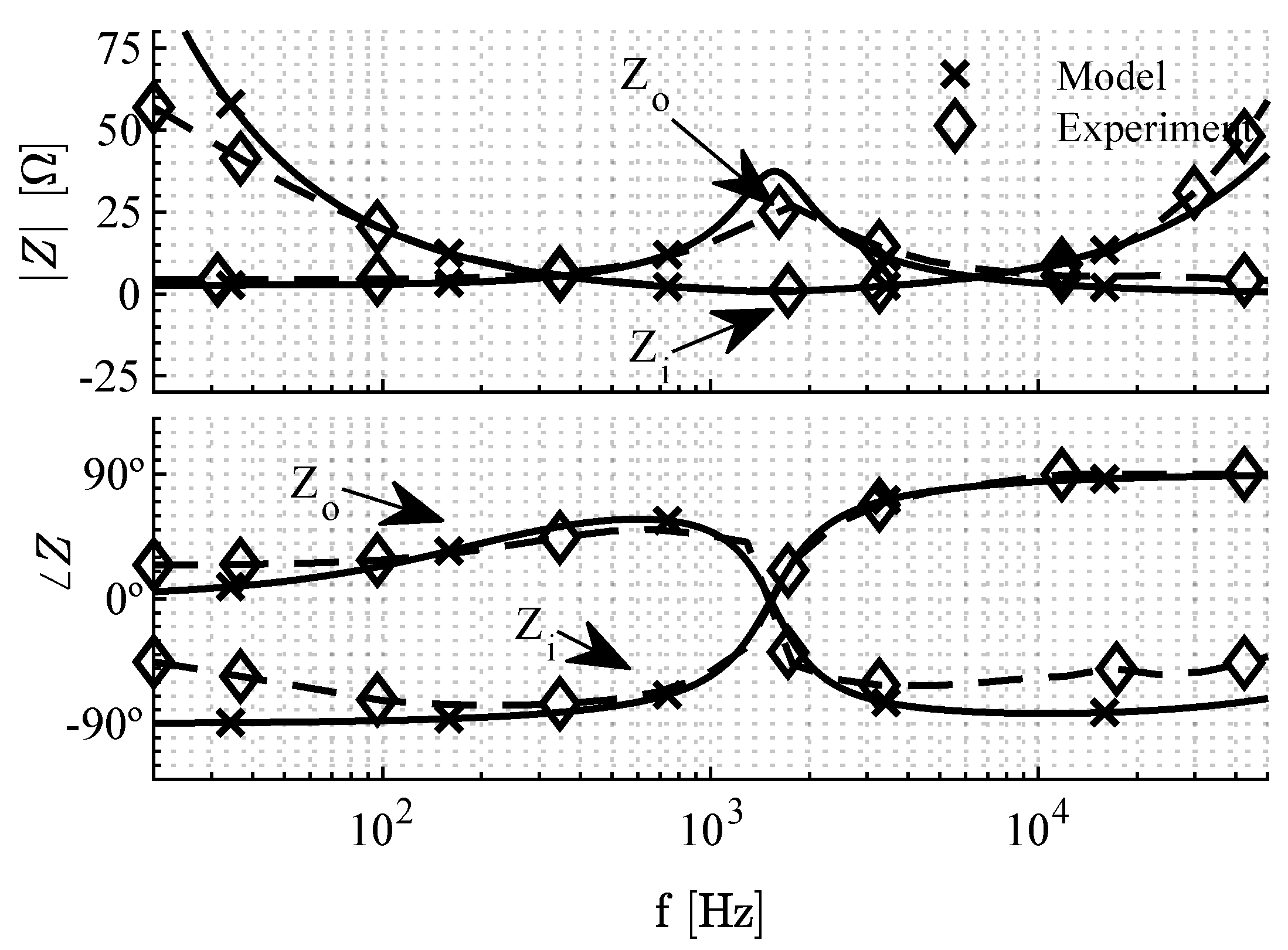
  • Experimental verification of the line-to-output transfer function, control-to-output transfer function, open-loop input impedance, and open-loop output impedance;
  • Design of a voltage mode controller in the synchronous reference frame and selection of controller parameters;
  • Estimation of loss and efficiency of the system.
The rest of the paper is organized as follows: Section 2 discusses the basics of the boost inverter operation using the duty cycle variation. Accurate mathematical models are proposed describing the converter dynamics in Section 3. The voltage mode controller design is explained in Section 4. Finally, the results from the simulation and the experimental procedure are presented with discussions in Section 5.

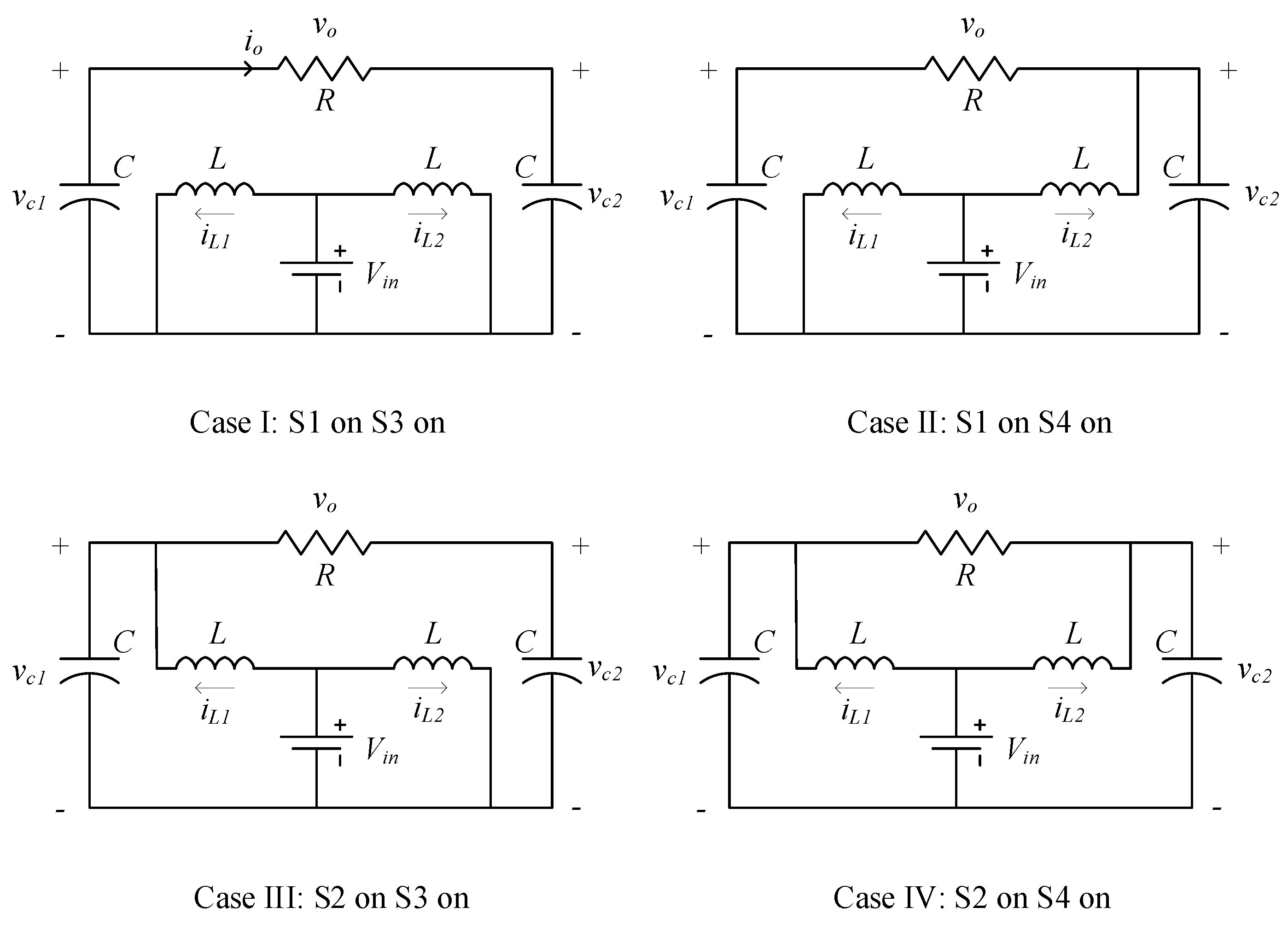
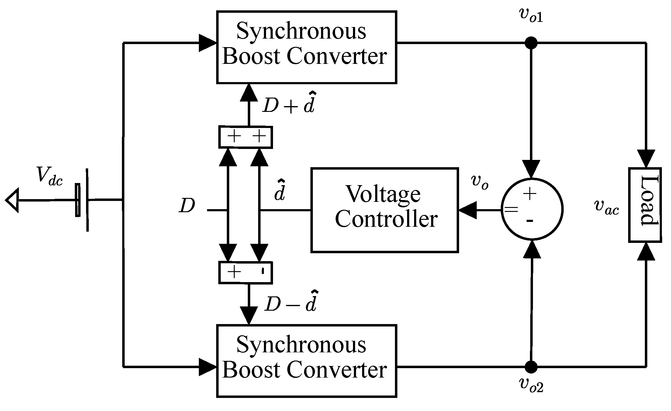
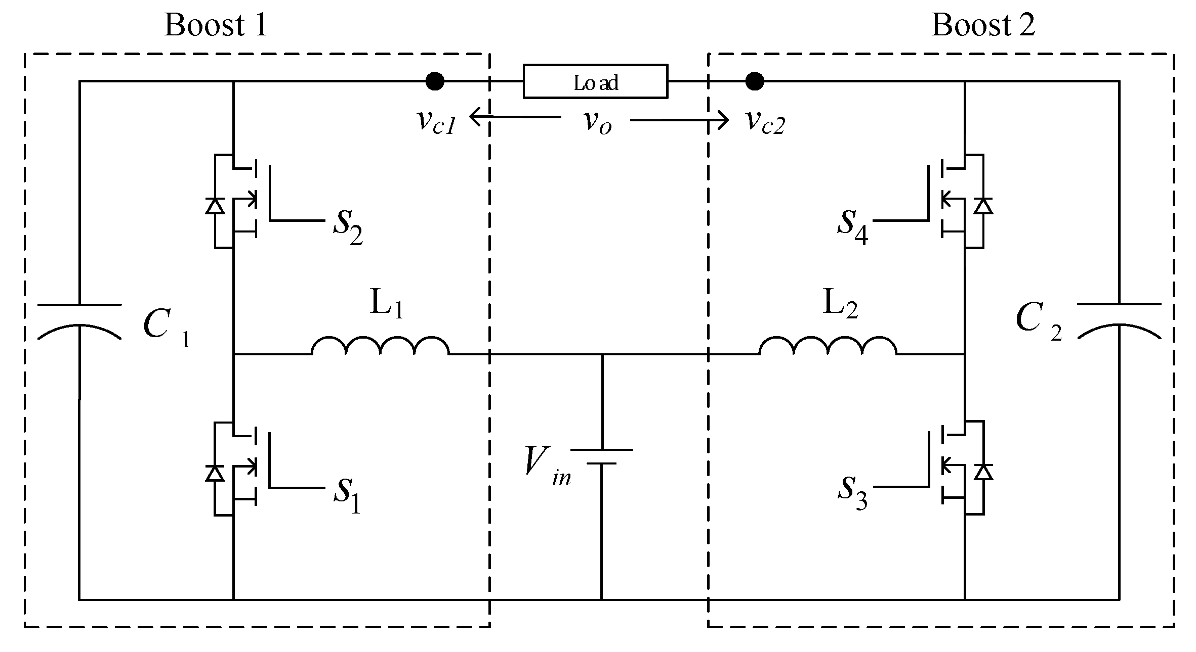
2. Basics of a Boost Inverter

The boost inverter proposed by Cacéres [2] is provided in Figure 1. The inverter uses two synchronous boost converters, marked as “Boost 1” and “Boost 2”, that enable continuous current flow with no zero states or discontinuous conduction. The original model was proposed based on the assumption that the values of the passive components are identical in both the converters. In practice, inductor values are chosen such that L 1 = L 2 = L and capacitor values are chosen as C 1 = C 2 = C . The boost sections are controlled separately to produce output voltages, v c 1 and v c 2 , appearing across the respective capacitors. The controllers are coordinated in a way that v c 1 and v c 2 are phase-shifted by 180° at all times, i.e.,
v c 1 = V d c + V m 2 cos ω t
v c 2 = V d c + V m 2 cos ( ω t + π )
where, V d c denotes the dc offset voltage, V m is the magnitude of the ac output, and ω is the nominal operating frequency in rad/s. If the load is connected across the capacitors, the final output voltage across the load is:
v o = v c 1 v c 2 = V m cos ω t .
Notice the cancellation of the DC terms in (2). The cancellation occurs regardless of the power factor of the load. The output voltage has a magnitude that is twice of that of the one obtained from the individual converter’s AC portion.
The waveform analysis in [29] explains that the boost inverter switching may not be realized using only one duty cycle variation. Assuming duty cycles for the individual boost sections to be D a and D b respectively, four different cases can occur. These four cases are depicted in Figure 2.
Only two out of these four cases can result in a sinusoidal voltage at the output. The following discussion provides a graphical representation of the duty cycles D a and D b and their relationship to the boost inverter output.
At steady-state, a conventional DC-DC boost converter produces an output voltage higher than the input voltage. The output is a fixed DC voltage with some high frequency switching ripple that is within an acceptable limit defined in the design process. In this particular configuration, the inverter consists of two boost converters, each producing a sinusoidally varying signal at a frequency much lower than the switching frequency with some DC offset. As a result, the duty cycle variations are very similar to the ones depicted in Figure 3. With the expectation that the duty cycles vary sinusoidally, both the waveforms in Figure 3 need to be centered around D = 0.5 . That way the waveform symmetry is preserved as the waveforms neither clip at the floor nor saturates at the top. In that case, the AC variation has an amplitude of d ^ . These two duty cycle variations, D a and D b , maintain a 180° phase shift with respect to each other. To generalize the duty cycle variation expressions considering D a = d = D + d ^ , the relationship between the duty cycles is:
D b = 1 D a = 1 ( D + d ^ ) = D d ^ = d ^
where, D = D = 0.5 .
This outcome indicates that Boost 1 inductor stores energy at the same time when Boost 2 inductor transfers energy to the load during 0 ω t < π . This process reverses during the next half cycle when π ω t < 2 π . The boost inverter operation is then limited to only two modes, Q s and Q s . The switching signals S 1 and S 4 have identical switch commands Q s , whereas switching signals S 2 and S 3 have commands Q s . This simplifies the mathematical modeling of the inverter to a great extent. The following section proposes a steady-state equivalent model and a small-signal model of the inverter system considering the component parasitic.

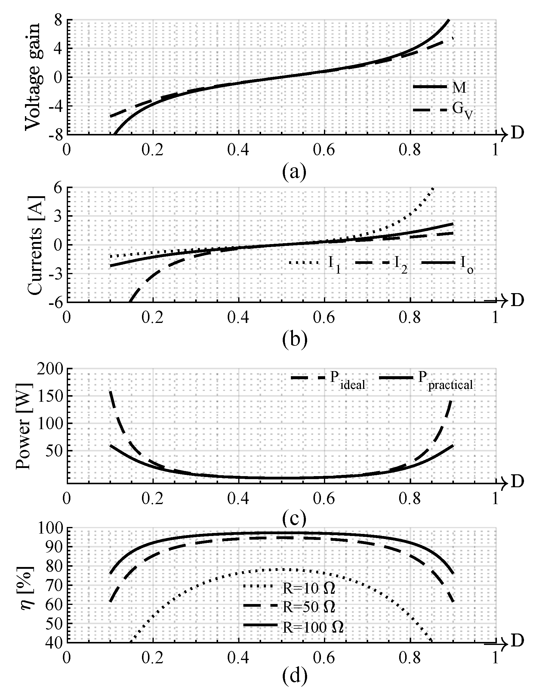
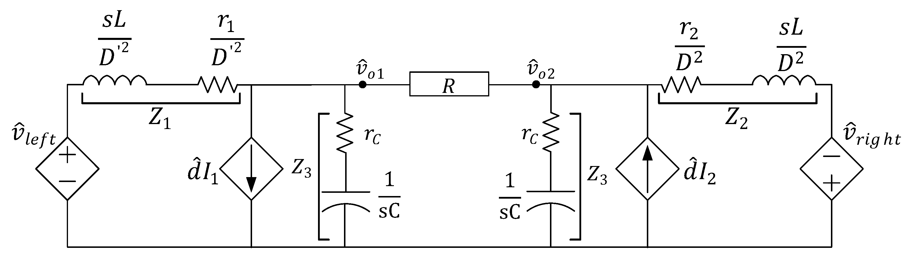
3. Mathematical Modeling of the System

The operating modes of the boost inverter are depicted in Figure 4. For the sake of simplicity, “Load” will be replaced by a linear resistor, R, during the discussion. The parameter definitions are provided in Table 1. The average current through the left capacitor over a complete cycle is:
I C 1 = 0 = D V o R + D ( I 1 V o R ) .
From which the value of I 1 is obtained as:
I 1 = V o D R .
Following the same method, the average value of the inductor voltage found from the left inductor over a complete cycle is:
V L 1 = 0 = D ( V i n ( r L + r D S ) I 1 ) + D ( V i n ( r L + r D S ) I 1 r C I C 1 V C 1 ) .
In the second time interval, I C 1 = I 1 V o R . From this and from (4) we obtain:
0 = V i n V o D R r 1 D ( V C 1 V o R r C )
where, r 1 = r L + r D S + D r C .
Similarly, the average current through the second capacitor is:
I C 2 = 0 = D V o R + D ( I 2 V o R )
which results in the value of I 2 as:
I 2 = V o D R .
Finally, considering I C 2 = I 2 V o R in the first time interval and r 2 = r L + r D S + D r C the average value of the remaining inductor voltage over a complete cycle is:
V L 2 = 0 = D ( V i n ( r L + r D S ) I 2 r C I C 2 V C 2 ) + D ( V i n ( r L + r D S ) I 2 )
resulting in:
0 = V i n V o D R r 2 D ( V C 2 V o R r C ) .

3.1. Quasi-Steady-State Equivalent Circuit Modeling

Taking (4) through (7) into considerations, the steady-state equivalent model of the boost inverter is formulated. The proposed steady-state equivalent model of the inverter is presented in Figure 5. From Figure 5c the individual converter outputs are:
V o 1 = V C 1 V o R r C = V i n D r 1 D 2 V o R
V o 2 = V C 2 V o R r C = V i n D + r 2 D 2 V o R .
Since, the output voltage across the load resistor is V o = V o 1 V o 2 , after subtracting (9) from (8) and then rearranging the terms gives the output-to-input ratio as:
G V = V o V i n = 2 D 1 D ( 1 D ) × 1 1 + 1 R r 1 D 2 + r 2 D 2 .
If the loss terms are not included, the voltage gain in (10) simply contains the gain factor M where, M = 2 D 1 D ( 1 D ) .
After substituting the parameter values from Table 1 the steady-state characteristic plots are obtained for different values of duty cycles. They are presented in Figure 6. The plot for G V in Figure 6a shows that at D = 0.5 the output-to-input ratio becomes zero.
The voltage gain lines, G V and M, start to deviate away from linearity noticeably below D = 0.2 and above D = 0.8 . Those are the practical limits of the inverter duty cycle. The gain curves match very closely between 0.25 D 0.75 . To know the current limits of individual converters, inductor currents at different duty cycles are determined. Referring to (4) and (6), the individual inductor currents are:
I 1 = V i n R × 2 D 1 D ( 1 D ) 2 × 1 1 + 1 R r 1 D 2 + r 2 D 2
and I 2 = V i n R × 2 D 1 D 2 ( 1 D ) × 1 1 + 1 R r 1 D 2 + r 2 D 2 .
The two inductor currents, I 1 and I 2 , and the output current, I o , are plotted for varying duty cycles in Figure 6b. A significant increase in inductor currents is noticed outside the range of 0.3 D 0.7 . These currents follow non-linear characteristics for a wide range of duty cycle meaning that the inductor currents are non-sinusoidal for the most part of the inverter operation. However, the output current stays linear for a range determined by the G V curve in Figure 6a. The system conduction loss depends on I 1 , I 2 , and the component parasitic. Since, D I 1 = D I 2 the efficiency of the inverter is:
η = P o P i n = V o D I 1 V i n I 1 + I 2 × 100 = 1 1 + 1 R r 1 D 2 + r 2 D 2 × 100 % .
A comparison of active power output with and without the conduction losses is depicted in Figure 6c. As expected, the output power reduces significantly as the loss terms are included in the mathematical model. In Figure 6d, the system efficiency is presented at three different load values as the duty cycle is varied. With the increase in load resistance, fewer I 2 R losses occur due to low current through the component parasitic. The efficiency calculation in (13) is significant in determining the load value that can be used in this particular boost inverter arrangement. For an accurate determination of the system efficiency, the other forms of losses such as the switching loss, dead time loss, gate charge loss, core losses in the inductor, etc. are needed to be calculated. The relationship between equivalent resistances, r 1 and r 2 , due to the parasitic components of the circuit elements is:
r 2 = r 1 + r C ( 1 2 D ) .
At D = 0.5 , these two resistances become equal.

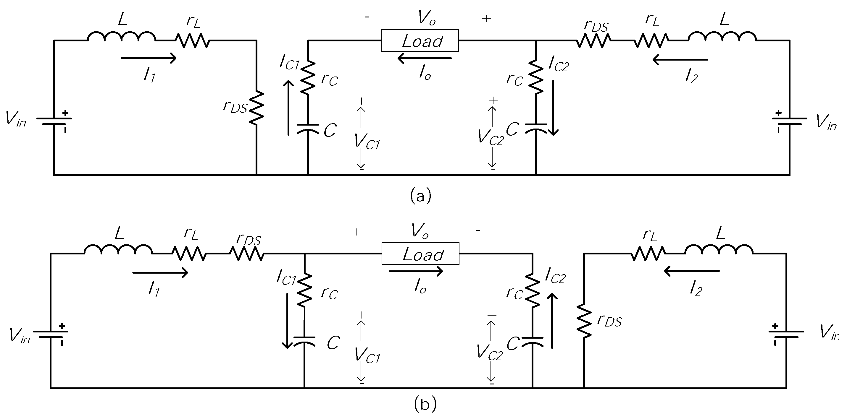
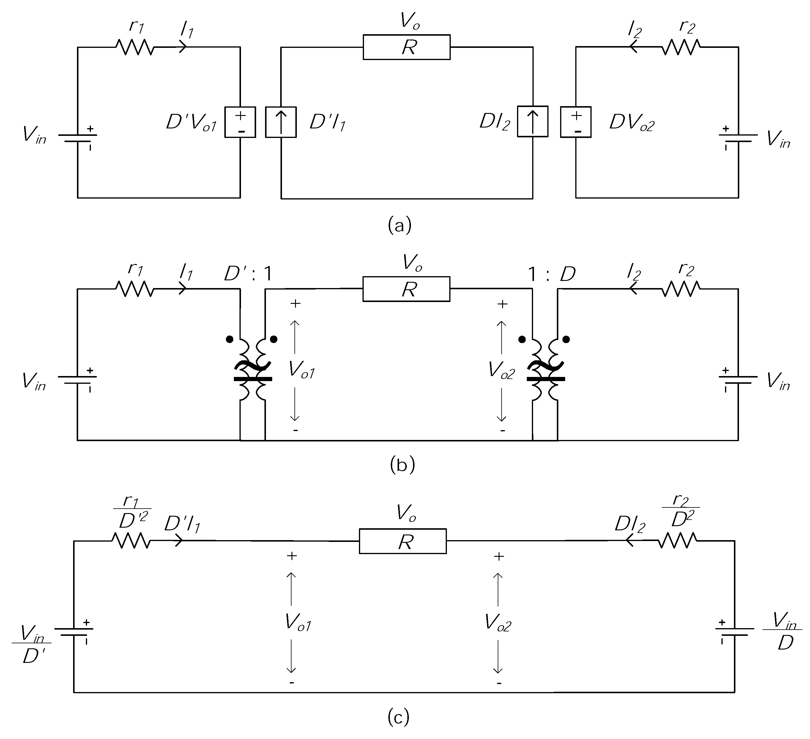
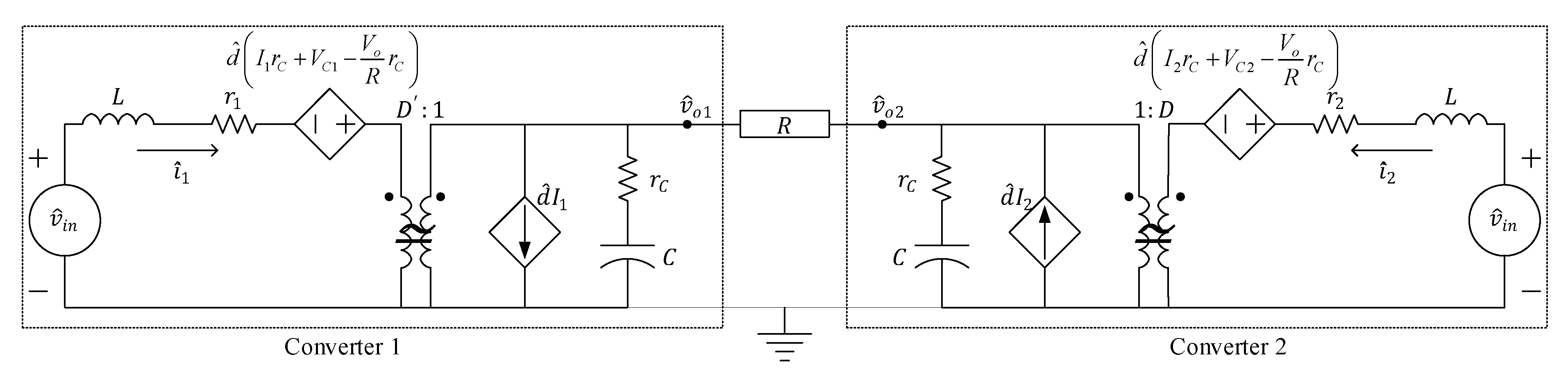
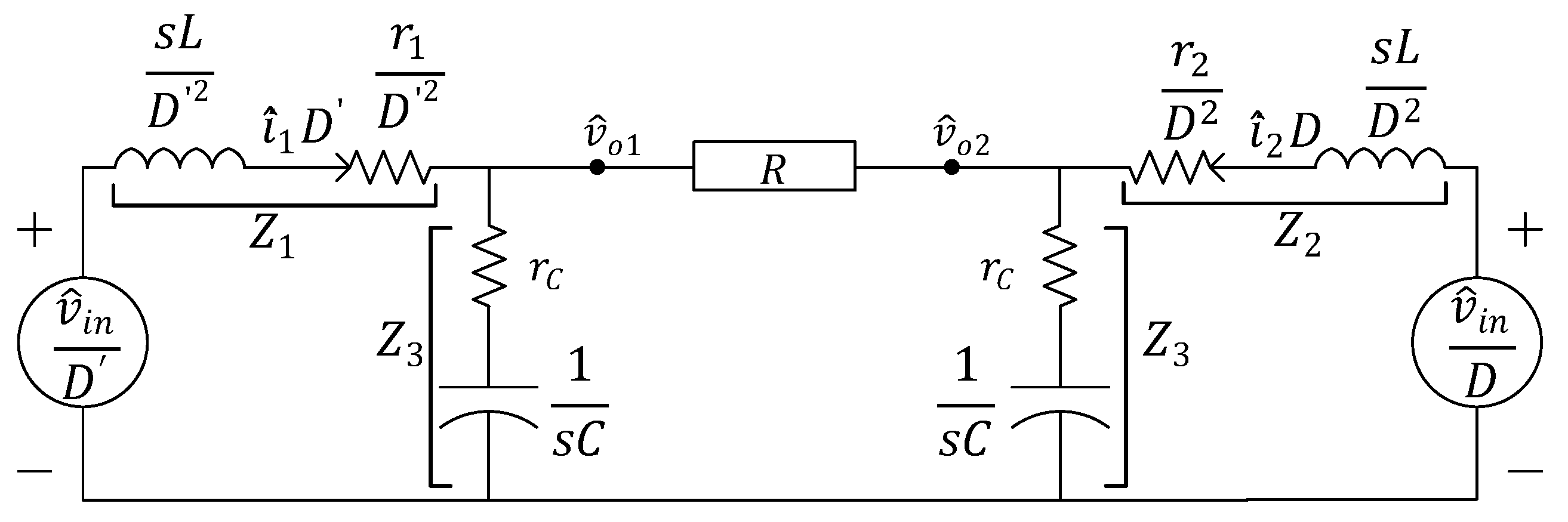
3.2. Small-Signal AC Modeling

The inverter small-signal AC model is obtained considering a small perturbation around the stable operating points. The quantities averaged over a cycle of the switching frequency, f s w , is the summation of the DC components and the AC: components
v i n = V i n + v ^ i n
v L 1 = V L 1 + v ^ L 1
i 1 = I 1 + i ^ 1
v L 2 = V L 2 + v ^ L 2
i 2 = I 2 + i ^ 2
v C 1 = V C 1 + v ^ C 1
i C 1 = I C 1 + i ^ C 1
v C 2 = V C 2 + v ^ C 2
i C 2 = I C 2 + i ^ C 2
d = D + d ^
d = D d ^ .
Substituting (15) through (25) in (4)–(7) and then equating the AC terms and neglecting the terms given by the product of two AC terms on both sides results in:
0 = v ^ i n + d ^ ( I 1 r C + V C 1 V o R r C ) i ^ 1 r 1 D ( v ^ C 1 v ^ o R r C )
0 = v ^ o R + d ^ I 1 D i ^ 1
0 = v ^ i n d ^ ( I 2 r C + V C 2 V o R r C ) i ^ 2 r 2 D ( v ^ C 2 v ^ o R r C )
0 = v ^ o R d ^ I 2 D i ^ 2 .
The small-signal AC model of the boost inverter is obtained based on the results in (26) through (29). The AC equivalent model is depicted in Figure 7 where, v ^ o 1 = v ^ C 1 v ^ o R r C and v ^ o 2 = v ^ C 2 v ^ o R r C .

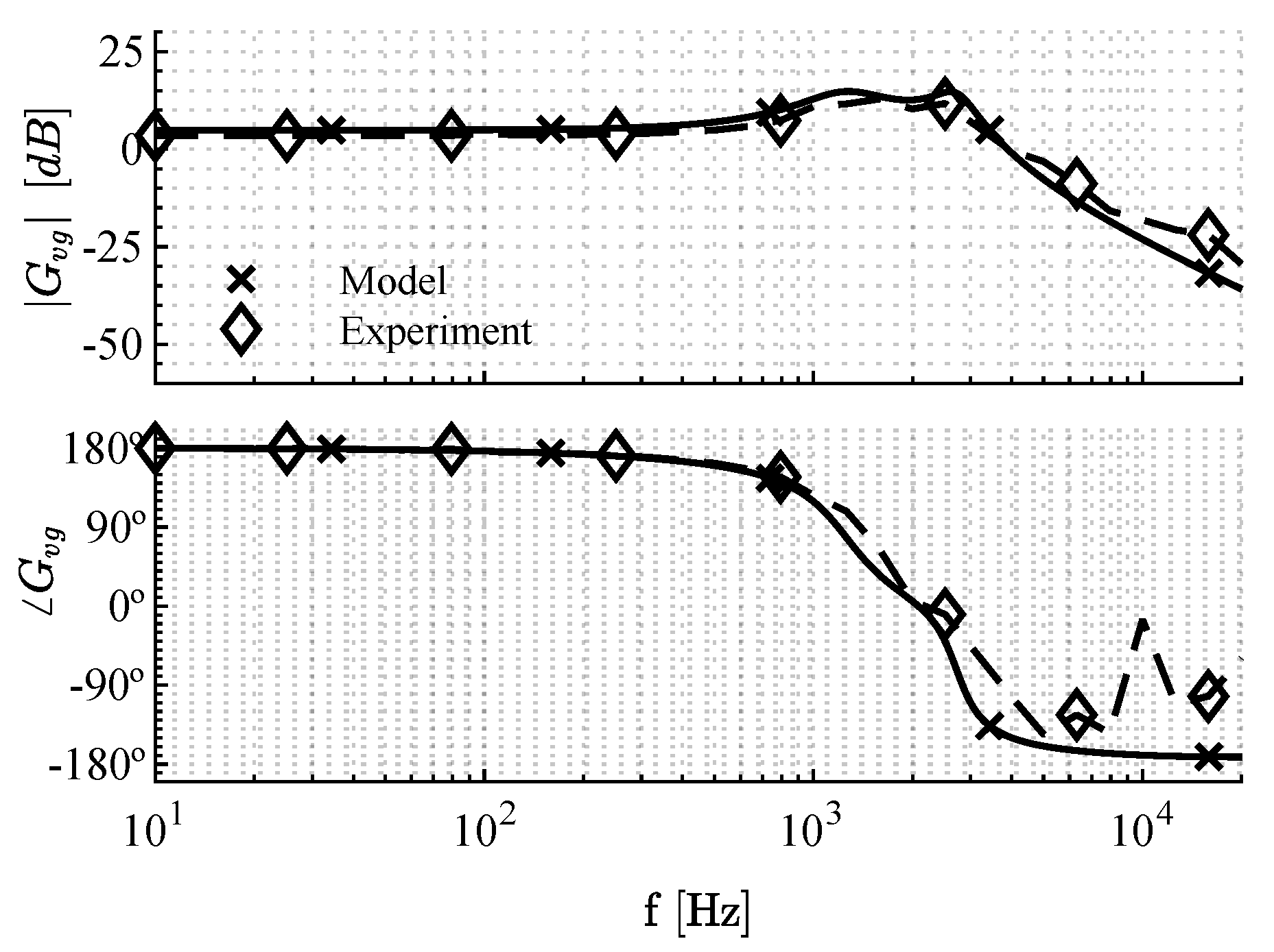
3.3. Line to Output Transfer Function

To obtain the line-to-output transfer function, G v g = v ^ o v ^ i n , the small-signal perturbation value d ^ is set to zero. The equivalent diagram is presented in Figure 8. After that, a Thévenin equivalent circuit with a source, v ^ t h , and an impedance, Z t h , is determined from the load’s perspective.
Removing the load and looking back from the load terminals the Thévenin’s equivalent impedance is:
Z t h = Z 1 | | Z 3 + Z 2 | | Z 3 .
where:
Z 1 = s L + r 1 D 2 ; Z 2 = s L + r 2 D 2 ; Z 3 = 1 s C + r C .
The Thévenin’s equivalent source is determined as:
v ^ t h = v ^ i n 1 D Z 3 Z 1 + Z 3 1 D Z 3 Z 2 + Z 3 .
Finally, applying the voltage divider rule, the line-to-output transfer function is:
G v g | d ^ = 0 = v ^ o v ^ i n = 1 D Z 3 Z 1 + Z 3 1 D Z 3 Z 2 + Z 3 1 1 + Z t h R .
It is interesting to note that the impedances Z 1 and Z 2 become equal at D = 0.5 . The expression then becomes equal to that of the one in (10). At D = 0.5 , the transfer function becomes equal to zero. That means this configuration is immune to any perturbation in the input source provided D (that is, the center point of duty ratio variation) always stays at 0.5. For any other values, any variation in the input will have an effect on the output response. The Bode plots in Figure 9 obtained from the small-signal model and the experimental results match closely at D = 0.7 . The Bode plots overlap for a large range of frequencies.

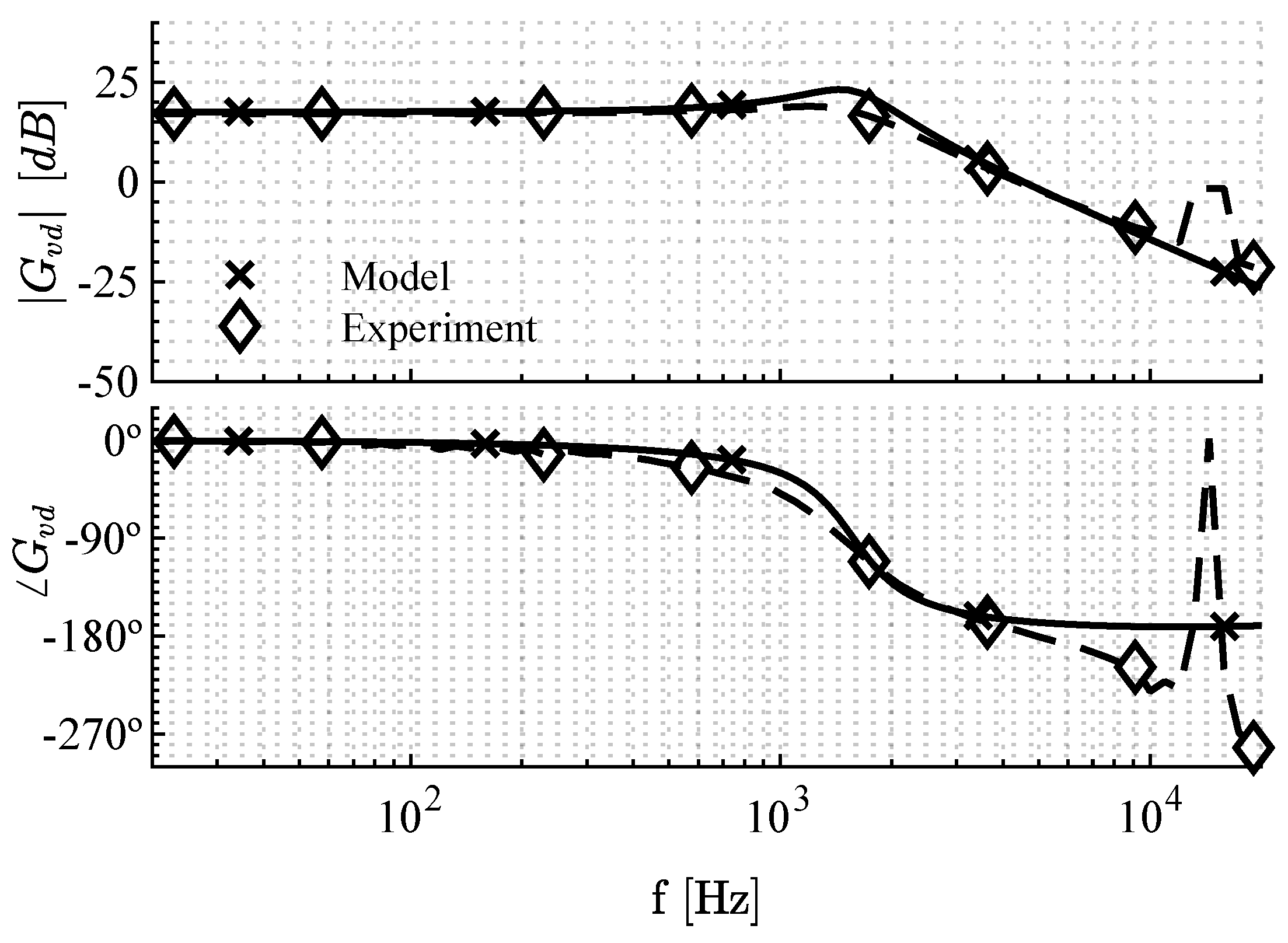
3.4. Control-to-Output Transfer Function

The control-to-output transfer function, G v d = v ^ o d ^ , is determined by setting v ^ i n to zero in the AC equivalent model. The equivalent diagram is given in Figure 10 where, v ^ l e f t and v ^ r i g h t are d ^ I 1 r C + V C 1 V o R r C / D and d ^ I 2 r C + V C 2 V o R r C / D respectively. After applying the source transformation technique and determining the equivalent current sources, the currents going into nodes v ^ 01 and v ^ 02 are:
i ^ l e f t = d ^ 1 Z 1 D I 1 r C + V C 1 V o R r C I 1
and
i ^ r i g h t = d ^ I 2 1 Z 2 D I 2 r C + V C 2 V o R r C
respectively. Since, the duty cycle is varied around 0.5, the average duty cycle becomes:
D = D = 0.5 .
This in turn results in:
Z 1 = Z 2 .
Moreover, from Figure 5c we obtain:
V o = 0 as a result , V C 1 = V C 2 ,
| I 1 | = | I 2 | .
The rest of the calculations are greatly simplified as i ^ l e f t becomes equal to i ^ r i g h t .
Afterwards, the superposition theorem is applied to the network to determine the node voltages considering one source at a time. With the presence of i ^ l e f t alone in the system, the equations relating to the node voltages are:
d ^ 1 Z 1 D I 1 r C + V C 1 I 1 = v ^ o 1 1 Z 1 | | Z 3 + 1 R + v ^ o 2 1 R
0 = v ^ o 1 1 R + v ^ o 2 1 Z 1 | | Z 3 + 1 R .
For simplified representation of the terms assuming:
β = 1 Z 1 D I 1 r C + V C 1 I 1
γ = 1 R
Δ = 1 Z 1 | | Z 3 + 1 R .
Solving (40) and (41):
v ^ o 1 d ^ = β Δ Δ 2 γ 2
and
v ^ o 2 d ^ = β γ Δ 2 γ 2 .
After that, considering the i ^ r i g h t source alone and following a similar approach gives:
v ^ o 1 d ^ = β γ Δ 2 γ 2
and
v ^ o 2 d ^ = β Δ Δ 2 γ 2 .
By considering (49) and by substituting in it (45) through (48) the control to output transfer function becomes:
v ^ o 1 d ^ + v ^ o 1 d ^ v ^ o 2 d ^ + v ^ o 2 d ^ = v ^ o d ^
G v d | v ^ i n = 0 = 2 β 1 Δ + γ .
The control-to-output transfer function in (50) is much less complicated compared to the transfer functions derived in [2] or [25]. Furthermore, the proposed transfer function includes the component parasitic resulting in an accurate mathematical model of the system. The complete expression of the transfer function is given in (51):
G v d ( s ) = 2 V i n × 1 + s C r C s 2 L C + 2 L C r C R + s 2 L R + 2 C r C r 1 R + D 2 C r C + C r 1 + 2 r 1 R + D 2 .
Ignoring the parasitic losses the transfer function becomes:
v ^ o d ^ = 2 D V C 1 I 1 s L s 2 L C + 2 s L R + D 2 = 2 V i n s 2 L C + 2 s L R + D 2 .
This helps to quickly determine the dominant poles of the system. It is interesting to note that unlike (52), the transfer function including the loss terms in (51) contains a zero. This results from using our assumption at (36) into (10) resulting in DC average values V o = 0 and I 1 = 0 from (5). This eliminates the zero and using (8) the numerator simply becomes 2 V i n . The physical interpretation of (52) is that when the individual DC-DC converters operate at an average duty cycle of 0.5, the average DC voltage output from both the converters becomes equal. Since the load is connected differentially, the average load voltage would then become zero which results in an average inductor current from each converter being zero. As a result, the right half-plane zero vanishes leaving the input voltage in the numerator with a gain factor of two.
The validity of the proposed transfer function is tested using the experimental test bed. The Bode plots of the control-to-output transfer function obtained using both the mathematical model and the experimental results are provided in Figure 11. The Bode magnitude and phase responses match closely. The only discrepancy that happens around 15 kHz is mainly due to the inclusion of the switching frequency during the experiment. However, this region is beyond the range where the averaging performed in preceding sections is valid. The resonant frequency occurs at:
ω o = 2 r 1 + D 2 R R L C + 2 L C r C .
The control-to-output Bode plot has a peak value that occurs at the resonant frequency, f r , of 1570 Hz and the measure of the dissipation in the system, Q = 5 dB from the model whereas from the experimental results it is 1.8 dB. Both f r and Q are impacted by the boost inverter capacitor selection. Figure 12 illustrates the impact of capacitance, C, and the capacitor ESR, r C , on the transfer function. Capacitance primarily affects the resonant frequency with only a modest impact on Q; whereas, ESR primarily affects Q with only a modest impact on f r . Thus a slight increase in ESR can substantially improve the transient behavior of the boost inverter by reducing Q. However, such a design selection can significantly impact converter efficiency. Therefore, ESR can be an important tradeoff to optimize.

3.5. Open-Loop Input Impedance

The open-loop input impedance, Z i , is determined after setting the duty cycle perturbation d ^ to zero. Under this condition, the equivalent diagram becomes very similar to that of the one presented in Figure 8. The equivalent voltage sources produce i ^ 1 and i ^ 2 through Z 1 and Z 2 respectively. The expression of the input impedance then becomes:
Z i = v ^ i i ^ 1 + i ^ 2 | d ^ = 0 .
Considering the current i ^ o flowing from node v ^ o 1 to node v ^ o 2 , the three mesh equations are:
( Z 1 + Z 3 ) D 0 Z 3 Z 3 D Z 3 D 2 Z 3 + R 0 ( Z 2 + Z 3 ) D Z 3 i ^ 1 i ^ 2 i ^ o = v ^ i n D 0 v ^ i n D .
This results in i ^ 1 v ^ i n , i ^ 2 v ^ i n , and v ^ i n i ^ 1 + i ^ 2 as follows:
i ^ 1 v ^ i n = Z 3 2 ( 2 D 1 ) + D R ( Z 2 + Z 3 ) + 2 D Z 2 Z 3 D D 2 ( Z 3 2 ( R + Z 1 + Z 2 ) + R ( Z 1 Z 2 + Z 1 Z 3 + Z 2 Z 3 ) + 2 Z 1 Z 2 Z 3 )
i ^ 2 v ^ i n = R Z 1 + R Z 3 + 2 Z 1 Z 3 Z 3 2 ( 2 D 1 ) D R ( Z 1 + Z 3 ) 2 D Z 1 Z 3 D 2 D ( Z 3 2 ( R + Z 1 + Z 2 ) + R ( Z 1 Z 2 + Z 1 Z 3 + Z 2 Z 3 ) + 2 Z 1 Z 2 Z 3 )
Z i = v ^ i n i ^ 1 + i ^ 2 = D 2 D 2 ( Z 3 2 ( R + Z 1 + Z 2 ) + R ( Z 1 Z 2 + Z 1 Z 3 + Z 2 Z 3 ) + 2 Z 1 Z 2 Z 3 ) R ( Z 1 + Z 3 ) ( 1 + 2 D ) + 2 D 2 Z 1 Z 3 + 2 D 2 Z 3 ( R + Z 2 ) Z 3 2 ( 4 D D 1 ) + D 2 R ( Z 1 + Z 2 ) .

3.6. Open-Loop Output Impedance

The open-loop output impedance of the boost inverter is determined considering perturbation at the load side. Considering d ^ = 0 and v ^ i n = 0 in Figure 7 the output impedance becomes:
Z o = v ^ o i ^ o | d ^ = 0 ; v ^ i n = 0 = ( Z 1 | | Z 3 + Z 2 | | Z 3 ) | | R .
Substituting (31) in (58) and in (59) gives the input impedance and output impedance transfer functions respectively. Furthermore, using the values listed in Table 1, the transfer functions Z i and Z o are determined at D = D = 0.5 . The corresponding Bode plots depicted in Figure 13 compares the small-signal results with the experimental results. The input impedance reaches the lowest value at a frequency that produces a resonating effect in the system. The output impedance becomes maximum at that same resonance frequency. Although, the magnitude plots match very closely, the phase plots show some deviation which can be largely attributed to the length of the cables attached to both the input and output sides of the inverter along with the possible impedance mismatch during the measurement.

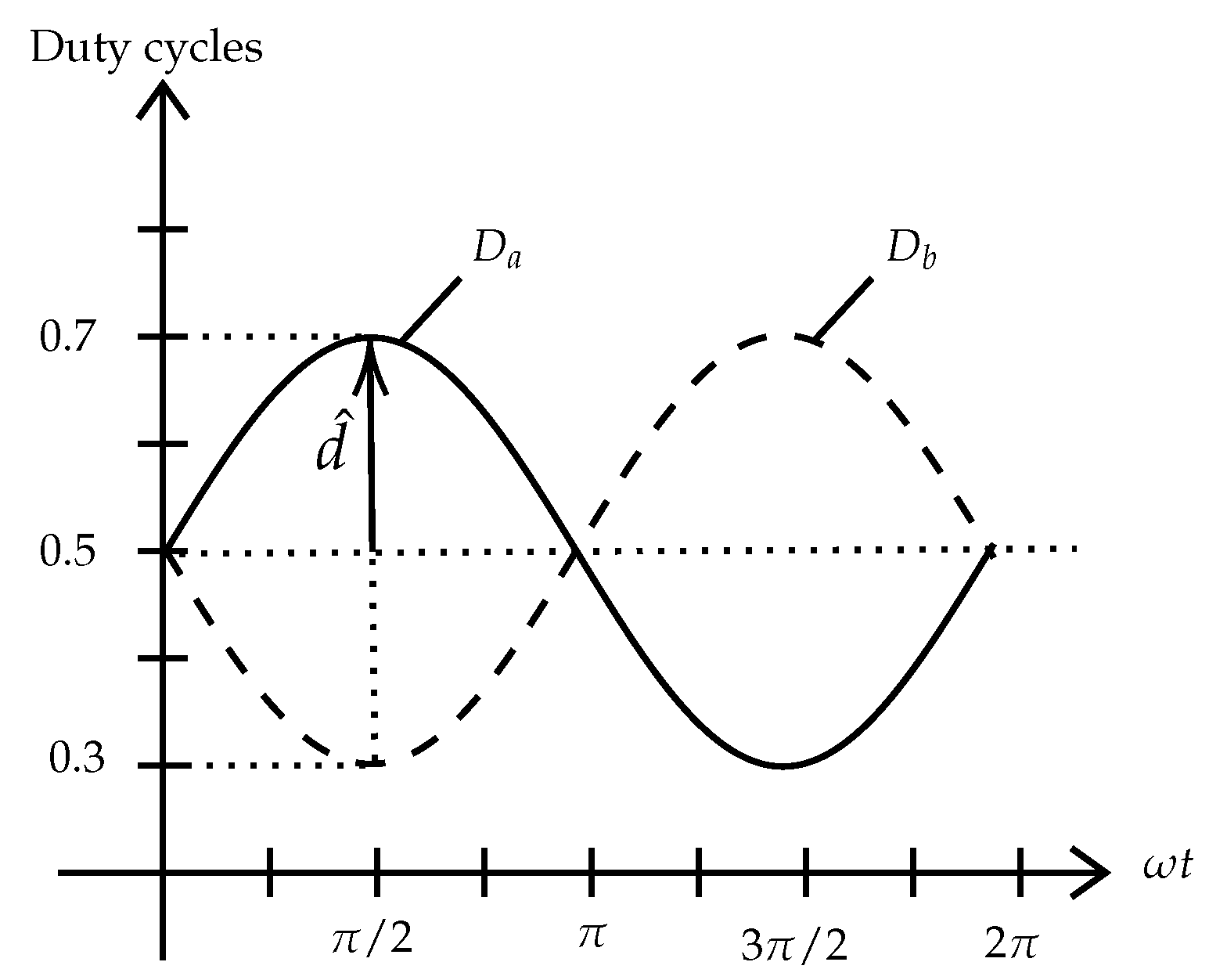
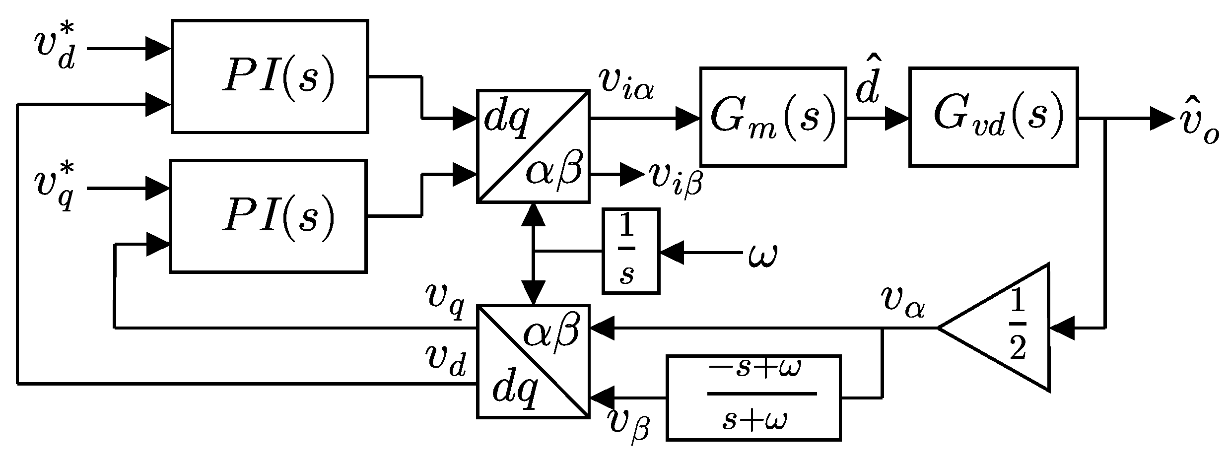
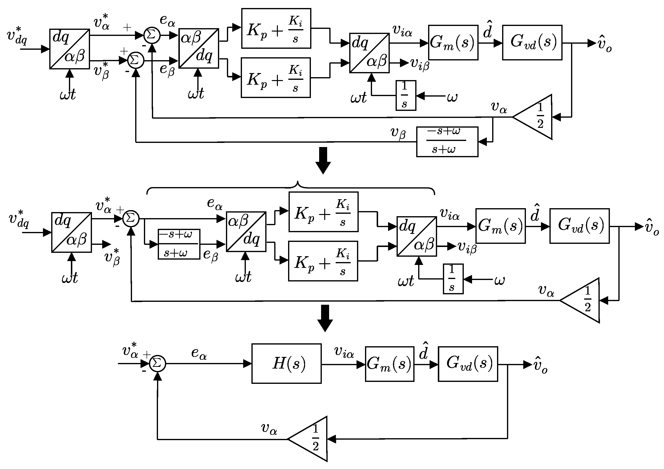
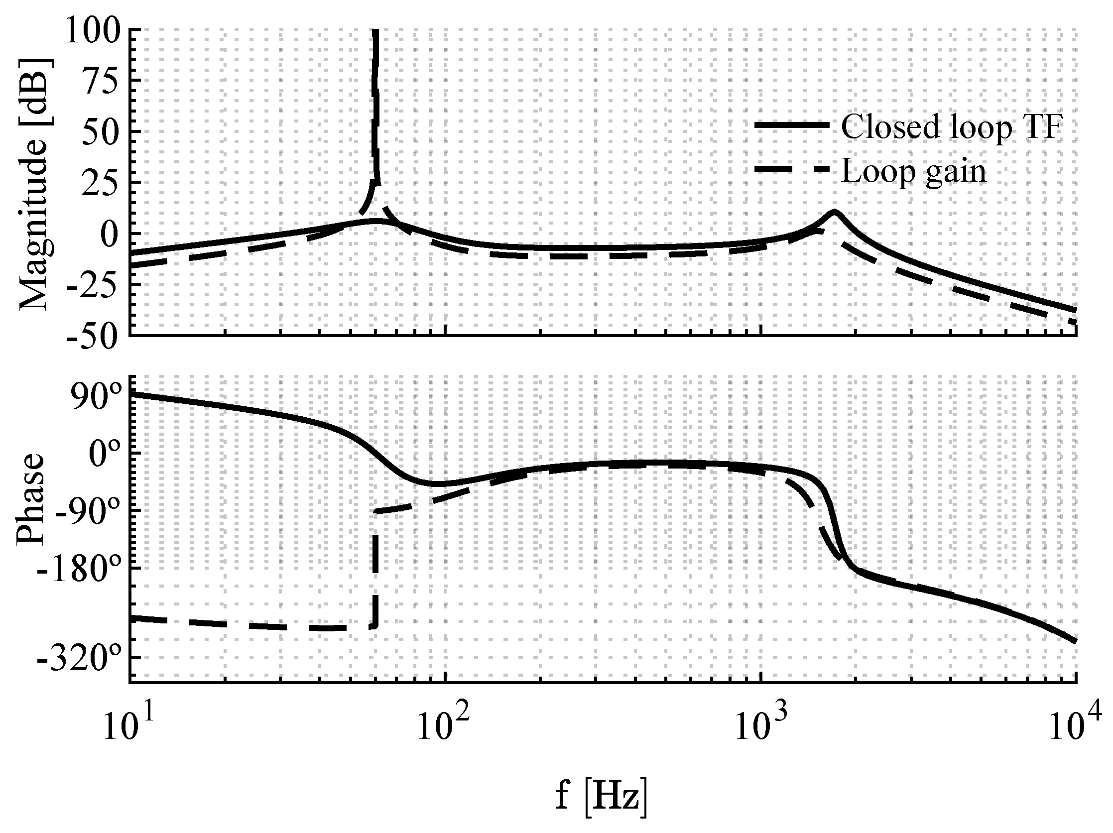
4. Voltage Mode Controller Design

In this section, the control-to-output transfer function in (51) is used to design a voltage mode controller for the boost inverter. A conventional voltage mode controller uses a simple proportional integral (PI) controller for reference tracking. However, this approach suffers from errors in terms of magnitude mismatch and phase delay when tracking a sinusoidal signal. For a precise reference tracking, the synchronous reference frame proportional integral (SRFPI) controllers are often deployed in power electronics. An SRFPI provides control over both the direct and quadrature axis components of the reference sine wave. The top view of the overall system architecture is depicted in Figure 14. Only one voltage controller is needed to operate the system. The output of this controller produces the required duty cycle variation d ^ . This variation is then combined with the fixed duty cycle D to produce the final duty cycles, D ± d ^ . The PWM signals for the respective boost converters are generated for controlling the individual boost sections.
The SRFPI voltage control algorithm applied to the current system is presented in Figure 15. The measured load voltage, v ^ o , is reduced by a factor of two because each converter produces half the output voltage. This scaled-down voltage is termed as v α . After that, a fictitious orthogonal signal, v β , is generated by applying an all-pass filter that produces a π 2 delay at ω :
G s h i f t ( s ) = s + ω s + ω .
The v α β signals are then converted into direct and quadrature axis components, v d and v q , using the Park transformation matrix:
T α β d q = cos ω t sin ω t sin ω t cos ω t .
The v d q signals are compared against the reference values, v d * and v q * . The resulting error signals are passed through the PI controllers. The PI controller outputs are transformed back to v i α and v i β using the inverse Park transformation matrix, T α β d q 1 . In the final step, v i α goes through the pulse-width-modulator to generate the switching signals. The transfer function of the PWM is:
G m ( s ) = 1 v d * e j ω T d
where, T d is the digital control delay and 1 v d * is the static gain. The overall system uses only one frequency, i.e., one time-base, as a reference.
Tuning an SRFPI controller is challenging. The process is simplified by first re-arranging the blocks in Figure 15 and then applying the well-known control theories. The simplified block diagram presented in Figure 16 has the reference expressed in the rotating reference frame.
The error signal, e β , is realized using (60) when the sinusoidal voltage is maintained at ω . The e β can be written in terms of e α as:
e β = v β * v β = G s h i f t ( v α * v α ) = G s h i f t · e α .
This results in an additional reduction in the block diagram as only v α * exists in the simplified model. Setting the q axis reference, v q * , to 0, the reference reduces to:
v α * = v d * cos ω t v q * sin ω t = v d * cos ω t .
A further simplification is performed following the same technique described in [30,31]. The stationary reference frame equivalent of the voltage loop is deduced as shown inside the curly braces in Figure 16. The transfer function relating the expected output voltage, v i α , to the voltage error, e α is:
H ( s ) = K p + K i s 2 + ω 2 s ω × 1 + ω s 1 + ω s .
The controller design objectives are: (a) The loop-gain bandwidth ( ω c ) is 1 9.21 of the switching frequency ( ω s w ) and (b) the ω c is achieved at a phase margin ( ϕ m ) of 45°. The loop gain of the simplified system is:
G o l ( s ) = H ( s ) × G m ( s ) × G v d ( s ) × 0.5 .
For faster calculations of regulator parameters, K p and K i , the H ( s ) can be approximated to:
H ( j ω c ) = K p + K i ω c 2 + ω 2 j ω c ω × 1 + ω j ω c 1 + ω j ω c K p + K i ω c 2 + ω 2 ( j ω c + ω )
| H ( s ) | | K p | .
This approximation is valid as long as ω c > ω and K p 2 K i ω c 2 . The condition ω c > ω is usually satisfied, since ω c is set about ω s w / 10 , and ω s w > > ω c .
Applying the values listed in Table 1 and Table 2 to (66) for an input voltage of 22 V and load reistance of 220 Ω and then setting | G o l ( j ω c ) | = 1 , the proportional gain becomes:
K p 0.077218 .
The parameter K i is calculated based on the phase margin requirement:
G o l ( j ω c ) = 180 ° + ϕ m .
Evaluating the angular contributions from (51) and (62), and using the value of K P in (65), the K i value is found from (69). The integral gain becomes:
K i 33.732   rad / s .
A quick check on the assumptions made earlier shows that ω c ( = 10.2   krad / s ) is 27 times greater than ω ( = 377   rad / s ) . In addition, the value of K p 2 ( = 0.006 ) is approximately 545 times larger than the value of K i / ω c 2 ( = 1.1 × 10 5 ) .
The closed-loop transfer function and the loop-gain Bode plots are depicted in Figure 17. A very high loop gain of 300 dB is achieved at the nominal frequency of 60 Hz. To observe the gain plots around 0 dB more closely, a truncated magnitude plot is presented. The phase plot confirms that the desired phase margin of 45° is obtained.

5. Results and Discussions

The inverter operation is tested with the newly designed regulator gains. The results obtained from the small-signal mathematical model, the full order PLECS simulation, and the experimental test bed are compared and discussed in this section.

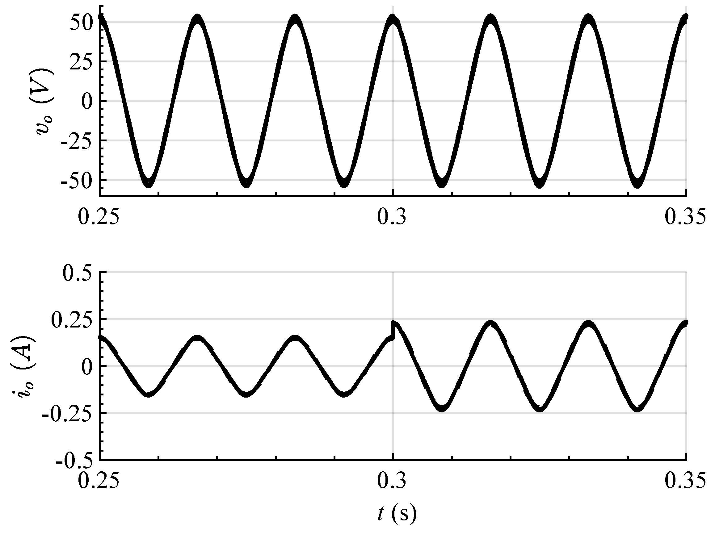
5.1. Simulation Results

Both the small-signal mathematical model and the full order model with the component parasitic are simulated in the PLECS platform. Three different perturbation cases are considered to check the system dynamics. These cases are discussed below.

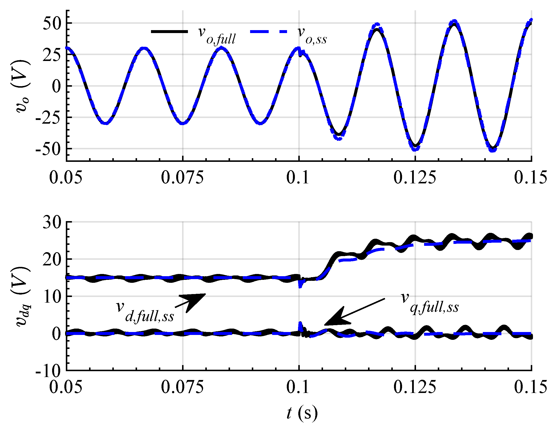
5.1.1. Change in Reference

A step-change in the reference voltage is made at t = 0.1   s . The input voltage is kept constant at 22 V. The output voltage reference v d * increases from 15 V to 25 V. Figure 18 shows that, as a consequence, the peak value of the output voltage increases from 30 V to 50 V. In Figure 18, the transient responses closely agree when the full order model results are matched with that of the one obtained from the small-signal (SS) model results. The transients cease within a cycle or two. After that, a zero steady-state error is maintained. The 15 kHz switching transients are visible in the v d q waveform. These switching ripples do not appear in the final output due to the natural low-pass filter characteristics of the inverter.
In Figure 19, the individual converter output voltages are depicted. The voltages represent an AC variation at the fundamental frequency added to a DC offset. The DC offset is equal in magnitude in both waveforms. The AC components are 180° out of phase.

5.1.2. Change in Input

A step change in the input from 22 V to 18 V is made at t = 0.2   s . The individual capacitor voltages and the final output voltage are shown in Figure 20. An expected drop in the DC offset is observable due to the fixed part, D, in the duty cycle. The output voltage level recovers fast and shows minimal change during this event.

5.1.3. Change in Output Impedance

Initially, a 343 Ω resistance is used as the load. At t = 0.3   s , a second load consisting of 690 Ω is added in parallel to the original one to get an equivalent of 229 Ω load. The output voltage and output current values are recorded and presented in Figure 21. The current magnitude increases during the step change in load. The output voltage remains steady throughout the event.

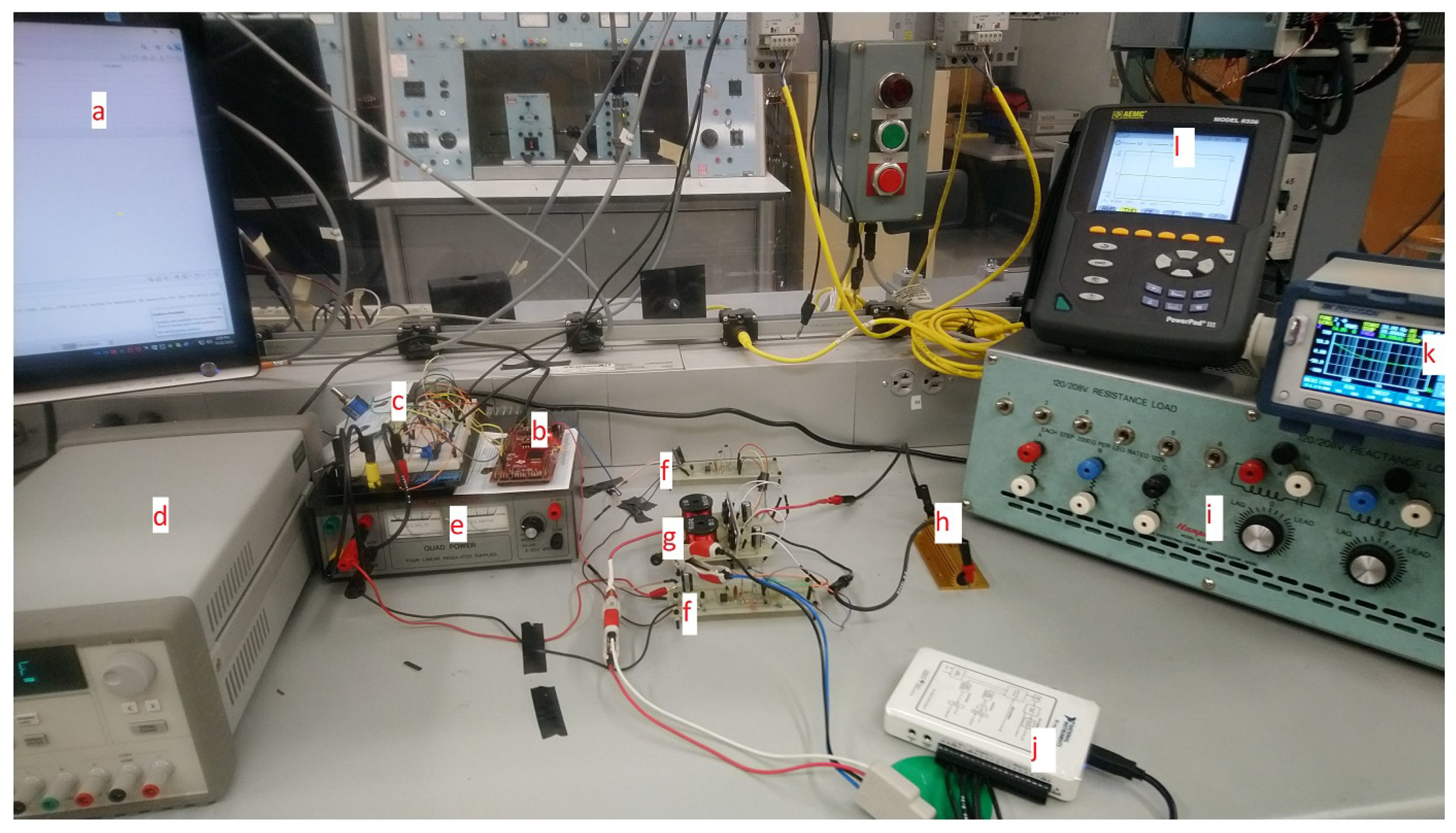
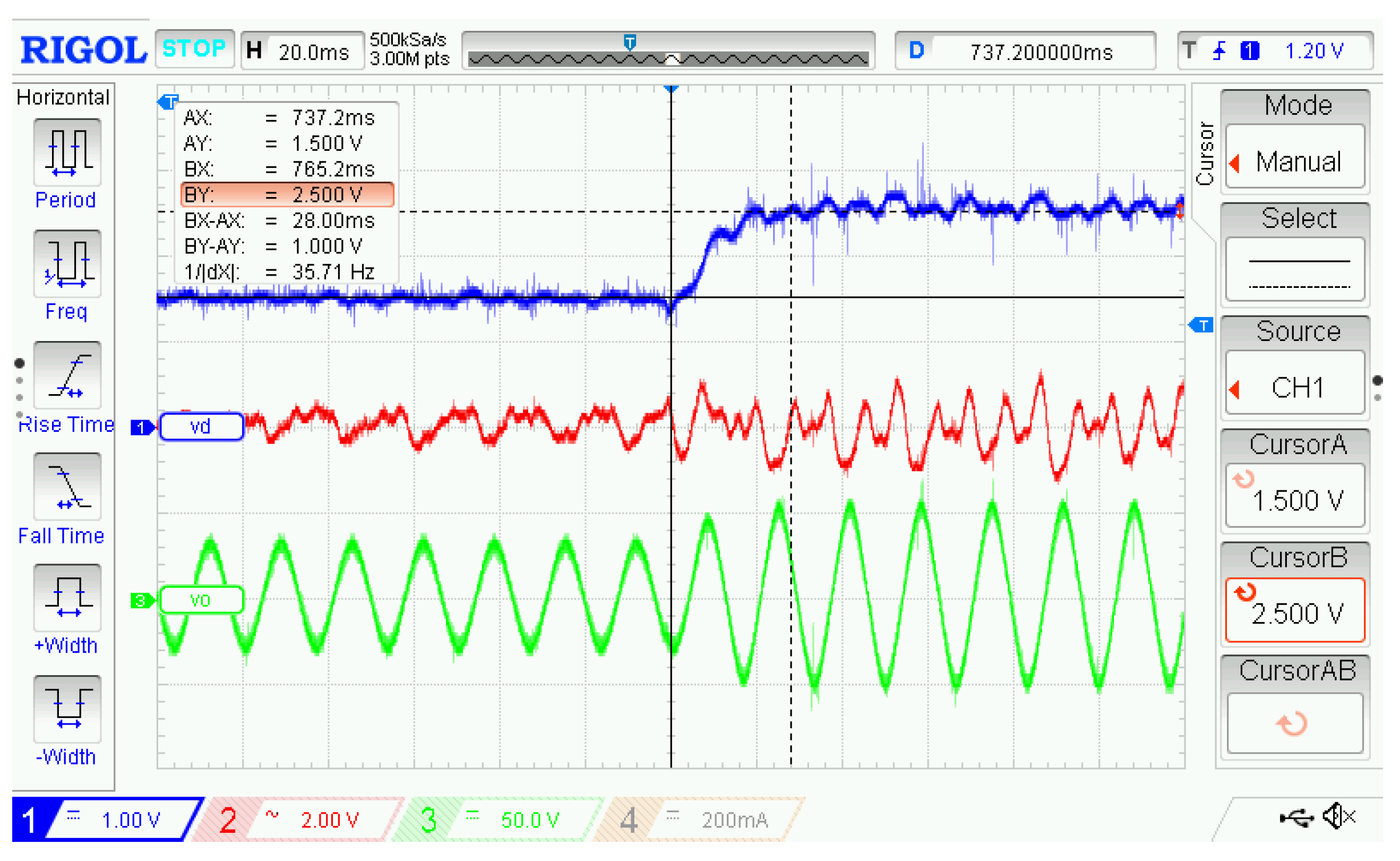
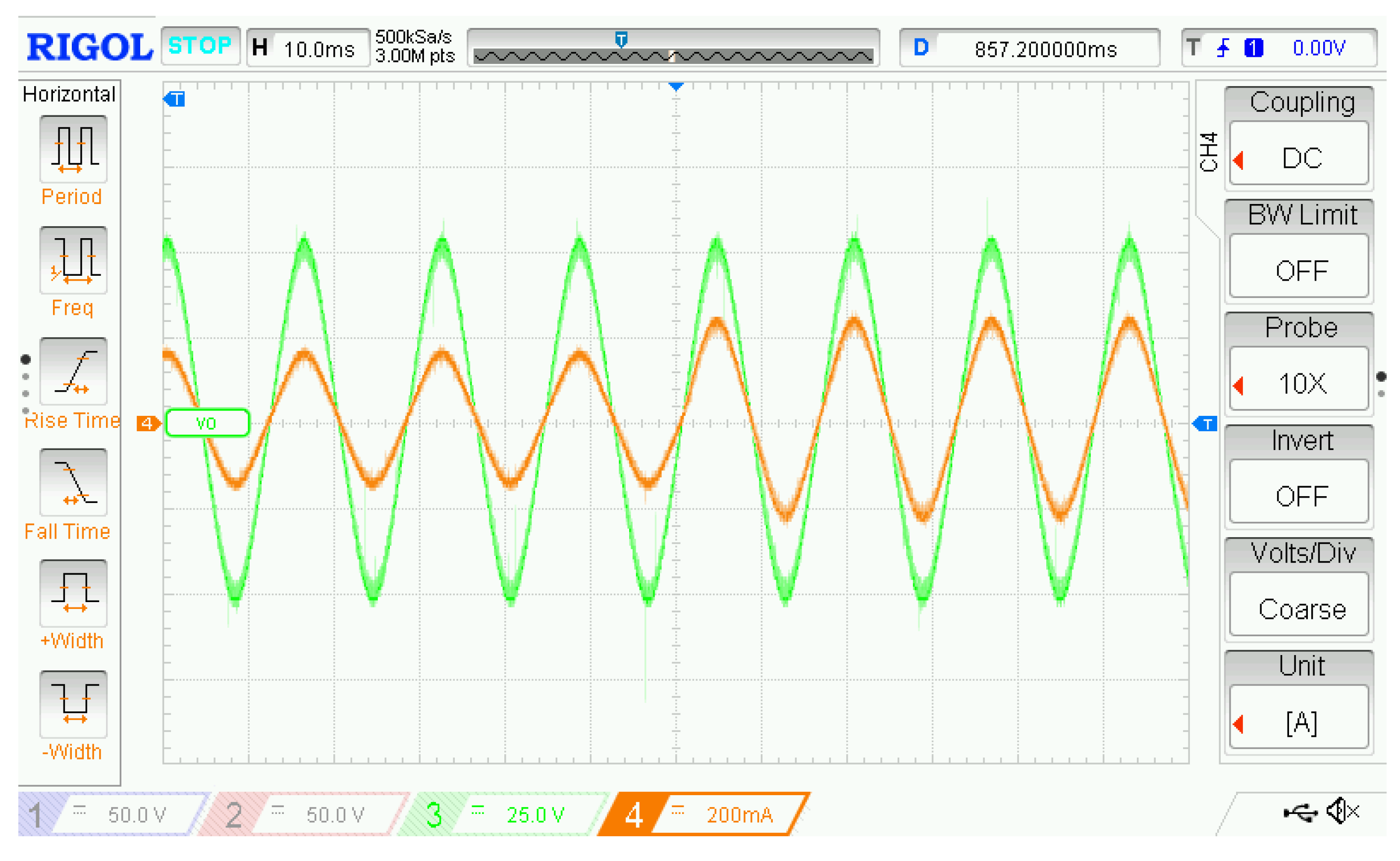
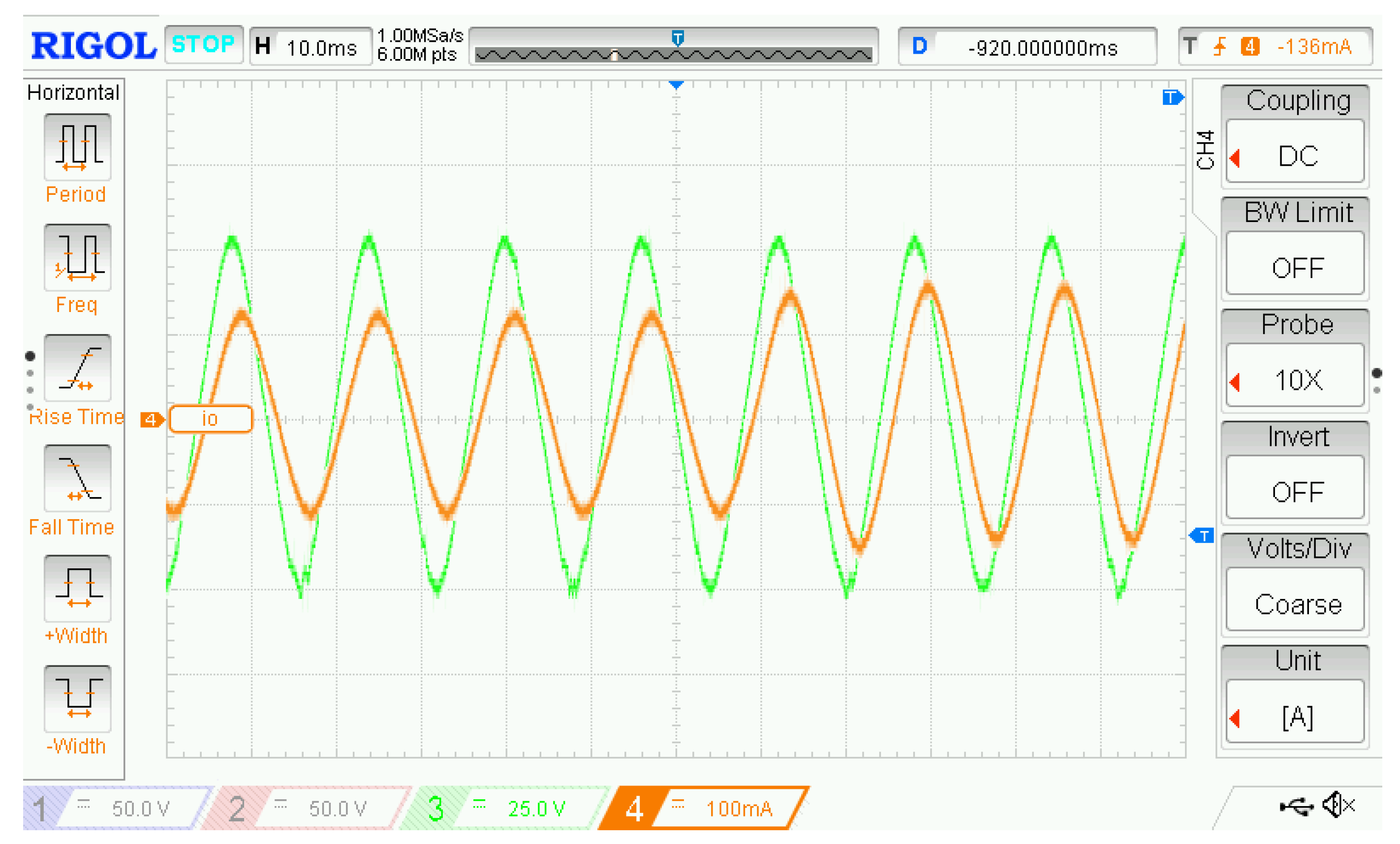
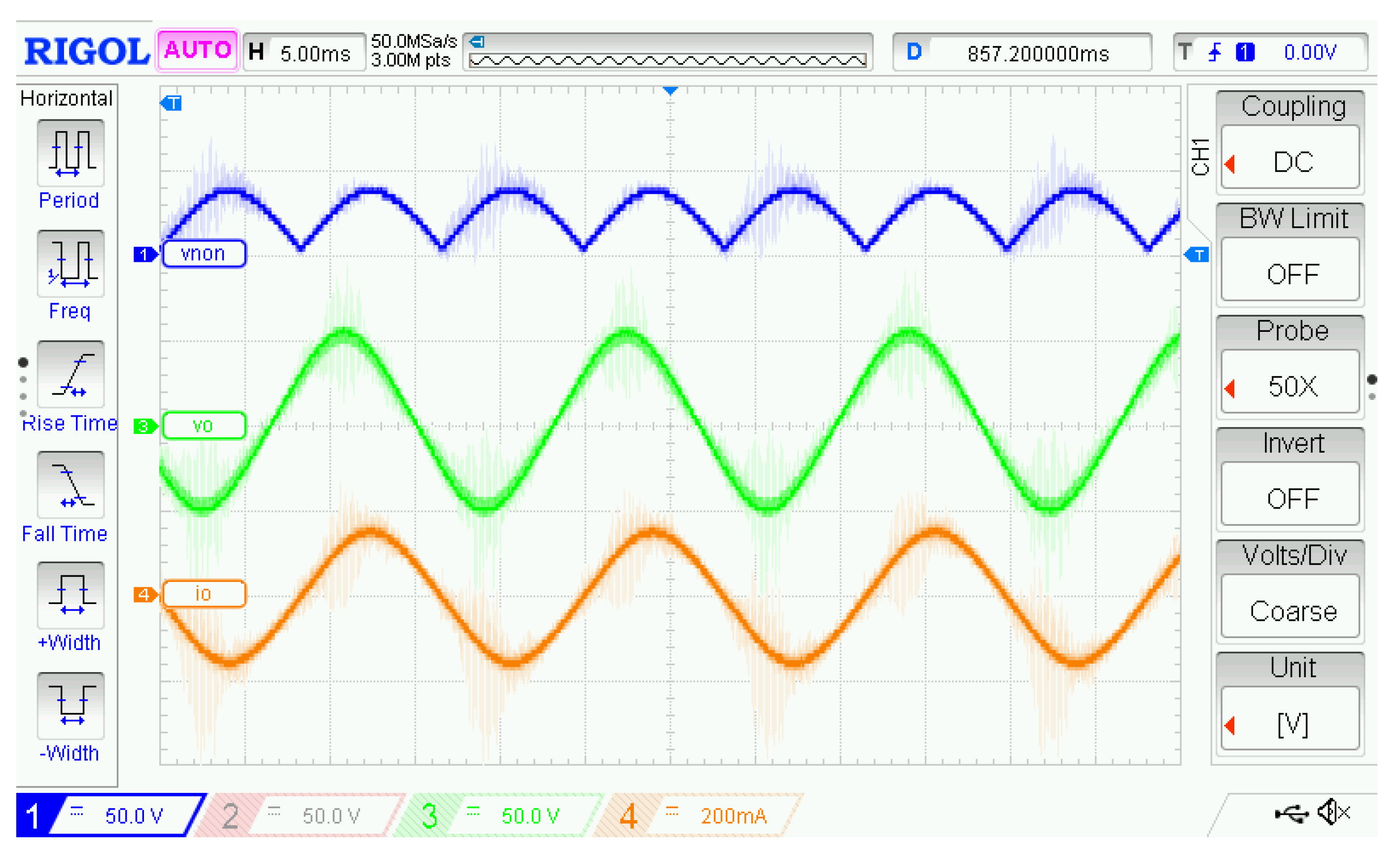
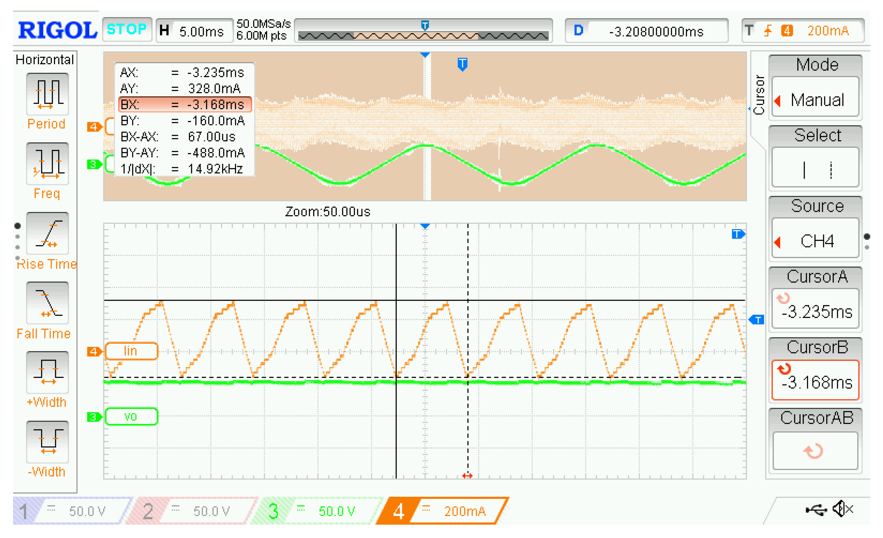
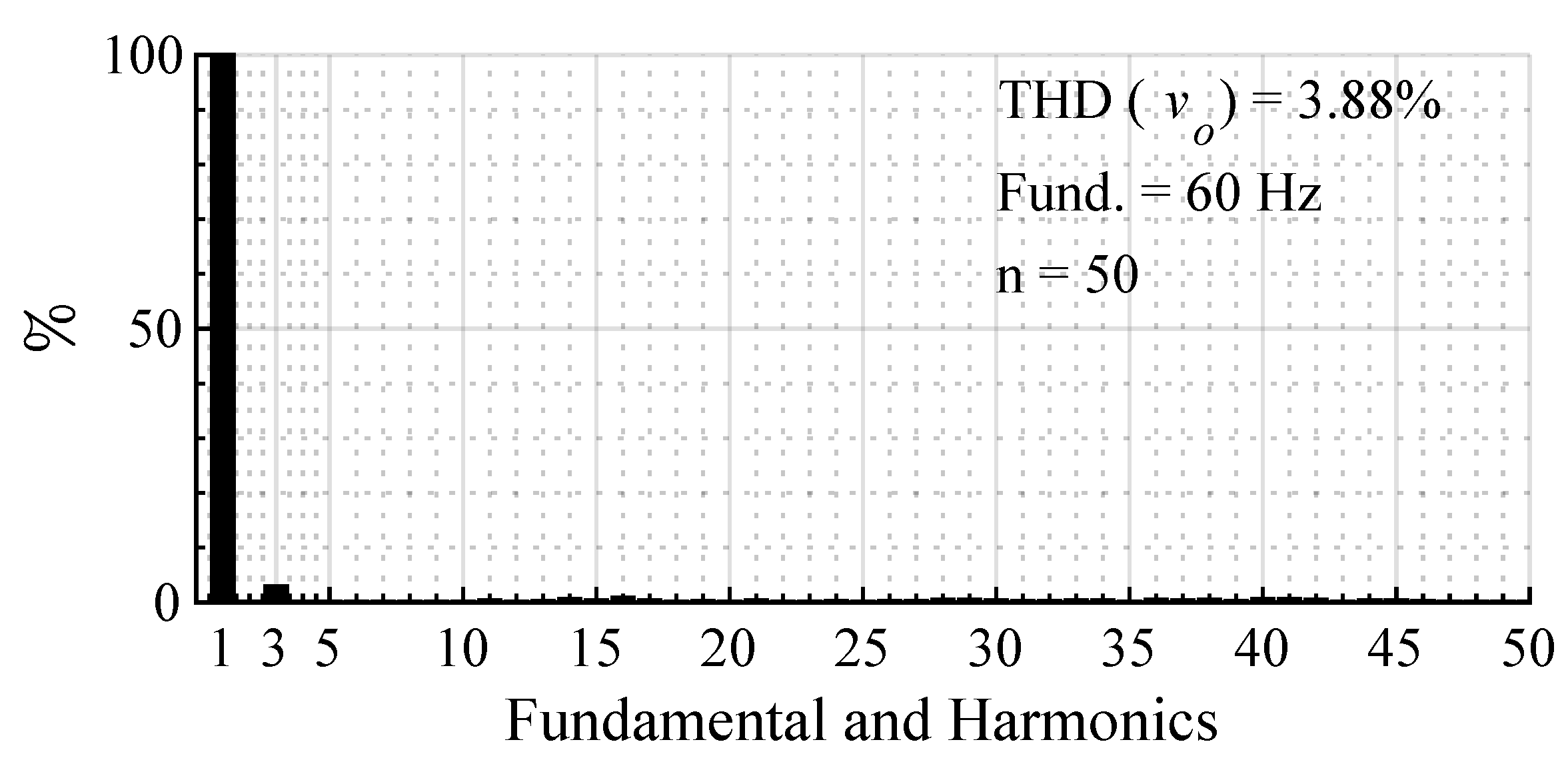
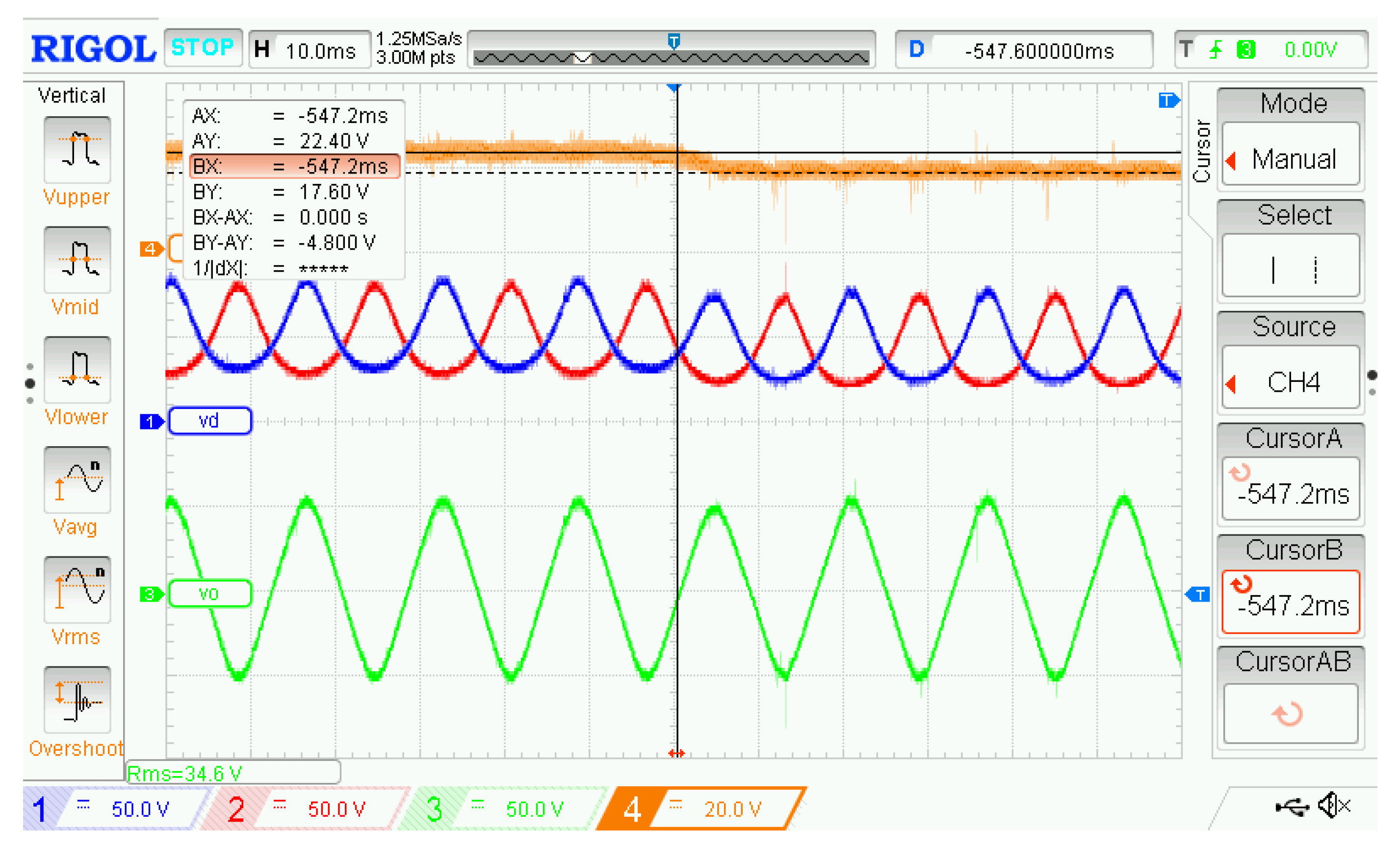
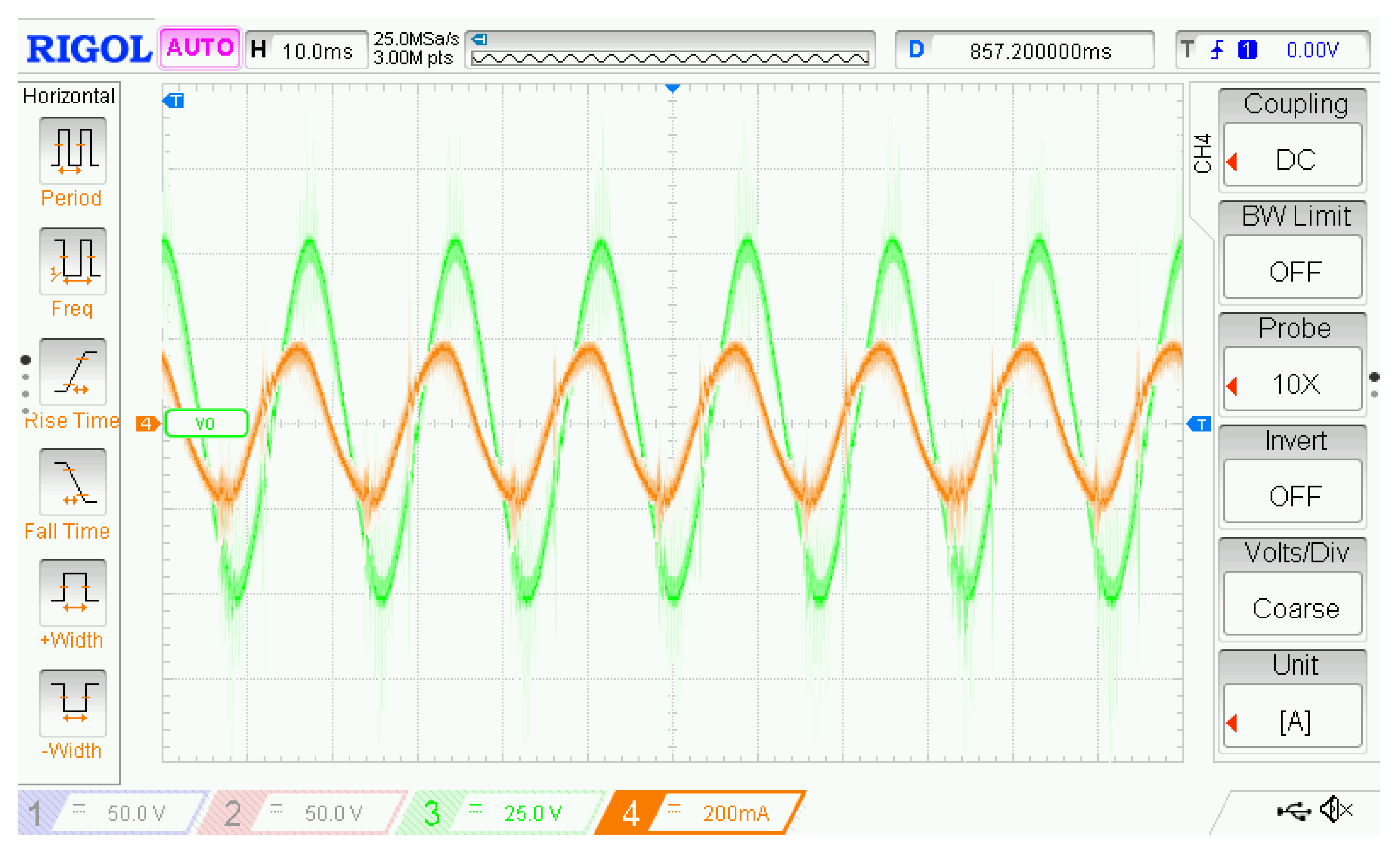
5.2. Experimental Results

The mathematical model and the controller gains are verified using a hardware testbed. The single-phase single-stage boost inverter discussed here consists of two DC-DC boost converters. The converters are designed with identical inductor and capacitor values. The selection of inductors and capacitors is made following the formulas provided in [32]. The controller algorithm is implemented using a Texas Instrument’s TMS320F28379D digital signal processor (DSP). The complete set up is depicted in Figure 22.
At first, the reference voltage, v d , is changed from 15 V to 25 V. In Figure 23, the output voltage magnitude changes from 30 V to 50 V. The d q axis voltage calculations are internal to the DSP. As a result, their measurement required first passing the variables through two separate PWM channels and then measuring them across an active low-pass filter output. The cut-off frequency of the filter was selected high enough to preserve the dynamics of the signals. A volt on the oscilloscope display means an actual measurement of 10 V. The q-axis voltage swings between positive to negative values with an average of 0 V. The transient in the v d q signal subsides within half-cycle. The dynamics match very closely with that of the ones presented in Figure 18.
In the second experiment, the DC input is reduced from 22 V to 18 V. This step change has a minimal effect on the output voltage as seen in Figure 24. The DC offsets in V C 1 and V C 2 drop as expected due to the fixed part in the duty cycle. The signal dynamics match very closely with that of the ones in Figure 20. The AC variations in the capacitor voltages are 180° out of phase.
In the next experiment, a step-change in load is provided. The new load values were mentioned previously. The change in load has not resulted in any change in the magnitude or in the phase of the output voltage as seen in Figure 25. The load current has increased when the new load is added in parallel to the system. Due to the drops in the switches and in the connecting terminals, the current magnitude varies slightly when compared to that of the one in Figure 21. The transients in the experimental results are once again consistent with the simulation results.
The inverter system is then tested using an RC load with the resistor and the capacitor values of 243 Ω and 15.4 μf respectively. The measurement of output voltage and current is presented in Figure 26. The current waveform leads the voltage waveform in this case.
The testbed is then subjected to an RLC load with the same resistor and capacitor values as mentioned previously. This time an inductor of 0.8 H is added to the system. The current in Figure 27 is lagging the voltage waveform, indicating that the load is more inductive. A step change in load is applied, which is noted by an increase in current magnitude.
A system is tested using a non-linear load. A full bridge rectifier is used to test the system. The waveforms in Figure 28 represent the inverter output voltage and output current along with the voltage measured across the diode bridge combination.
To demonstrate the switching ripple in the input current waveform, the measured input current in Figure 29 is zoomed at 50 us/div. The inset cursor measurement shows a 15 kHz ripple in the current output.
The total harmonic distortion (THD) of the output voltage is measured using an AEMC 8336 PowerPad III Power Quality Analyzer. The THD measurement is depicted in Figure 30. The measurement gives a THD value of 3.88% which is comparable to the values presented in [8,27,33]. When compared with the THD values reported in [8], the inverter discussed here has less THD level compared to the 2L-PWM and the 3L-PWM modulation techniques. However, in the same article, the L3L modulation technique shows better performance in terms of harmonics mitigation. The proportional resonant converter used to control the single-phase inverter in [33] provides a much higher THD level (11.8%) when compared to that of the one from the proposed controller. The THD values reported in [27] are slightly lower compared to the values measured in Figure 30 and below the limit mentioned in IEEE Std. 519-1992 [34]. However, the voltage control algorithm presented in this work shows a better performance in terms of tight regulation of output voltage magnitude. The peak-to-peak magnitude is maintained exactly at 100 V in this work compared to the one presented by Jha et al. which is 96 V. This is because there is a 300 dB gain at the operating frequency as shown in Figure 17. This high gain at the operating frequency is absent as shown in Figure 6 in [27] which results in a decreased magnitude at the operating frequency. Among the three voltage-mode controllers presented in their work, only two uses a negative feedback loop. In contrast to the method presented in this work (Figure 14), two different control loops are present and two different voltage references are required. The proposed method in this work needs only one set of references, v d q * , and compares the DC signals to generate errors that are passed through the PI controllers to produce the desired PWM signals. Whereas the control loop structure by Jha et al. uses a sinusoidal reference tracking mechanism. Using this scheme introduces steady-state amplitude and phase errors whenever a PI controller is used for tracking a sinusoidal reference signal. It is possible to reduce the error by increasing the controller gain. However, it compromises the system stability due to noise amplification.

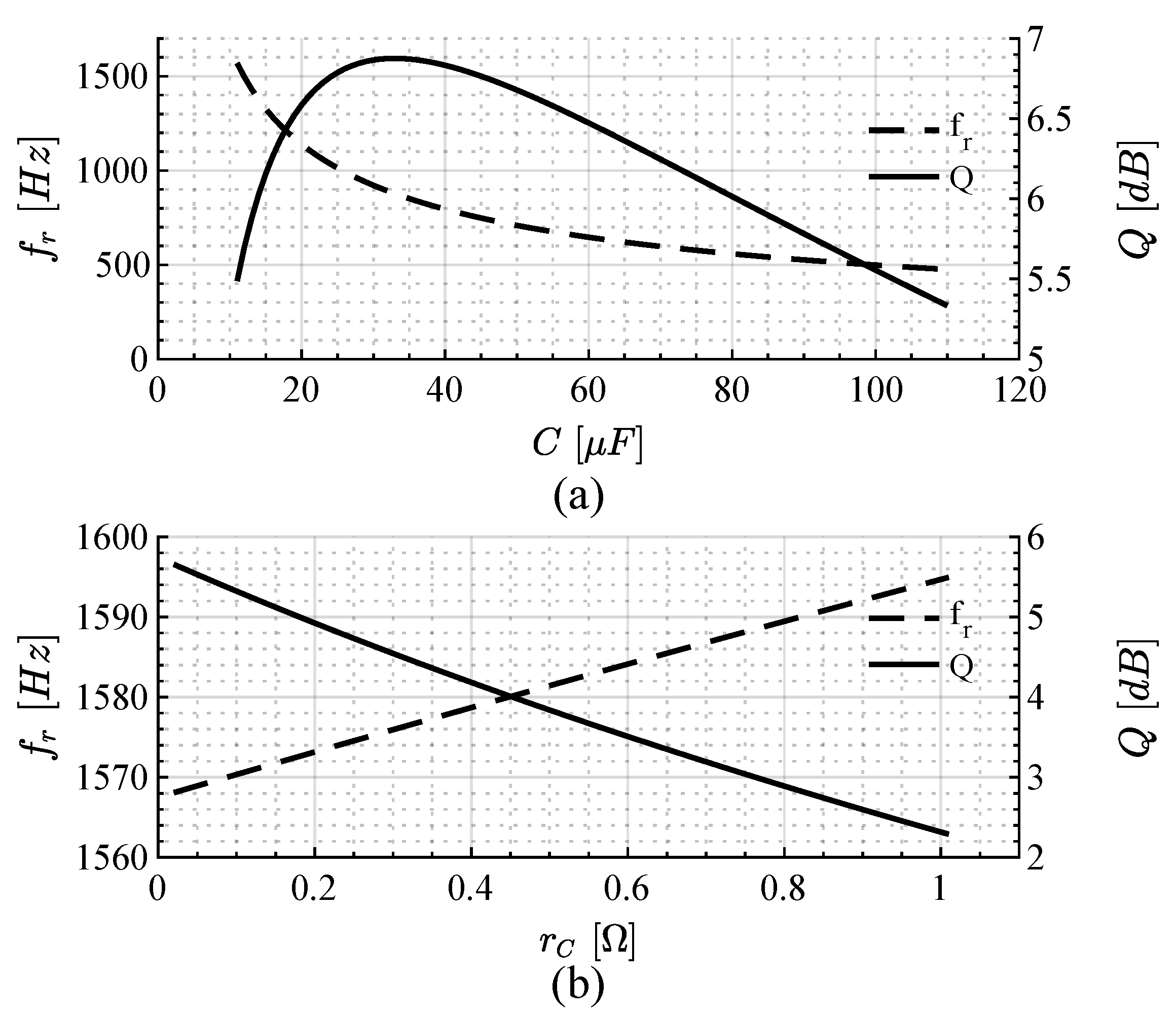
5.3. Stability Margins and Sensitivity

The minimum load impedance required for the system to remain stable at all frequencies can be obtained by applying the Middlebrook’s stability criterion. For that, the Thévenin equivalent output impedance of the inverter, Z o , t h , is determined from (59) by setting R = . The peak value of the output impedance magnitude under this condition is 43.2 dB. Thus, the system is locally stable if the magnitude of the load impedance, Z l o a d , is greater than 145 Ω. If impedance magnitudes are lower, then the system will still be stable provided that the impedance ratio of the transfer function, Z o , t h Z l o a d , satisfies the Nyquist stability test. The system stability margins for the closed-loop system in Section 4 are determined from the loop-gain Bode plot. The gain margin of the system is found to be approximately 8.43 dB at 1.62 kHz and the phase margin is found as 45° at 1.97 kHz.
To perform a sensitivity analysis, the closed-loop transfer function, G c l , is determined from (66). The sensitivity of G c l with respect to parasitic components, r L , r C , and r D S are determined as S r L , S r C , and S r D S respectively. The Bode plots respresenting the magnitude of these functions are given in Figure 31. It is observed that the system is less sensitive to changes in both r L and r D S at various frequencies. The sensitivity in both the cases becomes maximum at the resonant frequency which is expected. However, the magnitude of the sensitivity due to the different values of these two parasitic are tightly bounded in that region. The sensitivity due to the capacitor ESR, however, starts to increase as the frequency progresses. This indicates that several parallel capacitors are needed to be placed at the output side to reduce the overall r C .
The sensitivity analysis is then carried considering variations in L, C, and load resistor, R. The Bode plots corresponding to the sensitivity functions, S L , S C , and S R are shown in Figure 32. It can be noted that the closed-loop transfer function’s sensitivity is highly influenced by both the inductors and capacitors as the frequency approaches the resonant frequency and above. The sensitivity due to the load remains low at all frequencies other than the resonant peak as expected. The sensitivity in this case lowers as the load value is increased.
In all three cases, the sensitivity is lowest at 60 Hz.

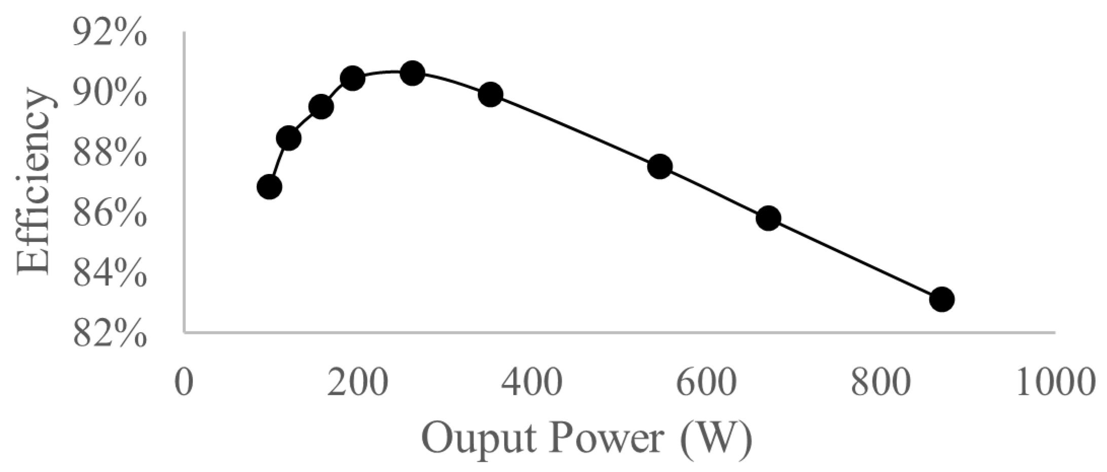
5.4. Loss Estimation and Efficiency

The two main sources of losses in this system are the semiconductor device losses and the inductor I 2 R losses. The low power inverter prototype in this work is constructed to verify the small-signal models and the controller algorithm. At this power level, the losses tend to dominate, resulting in poor system efficiency. To represent a practical system, the output voltage level is raised to 110 V r m s in the PLECS simulation platform. The system losses are then estimated using a high power MOSFET switch (C2M0025120D) for which a detailed thermal model suitable for PLECS simulation is readily available. The efficiency curve at different power levels in Figure 33 shows that the maximum efficiency occurs around 240 W. The loss breakdown for the inverter system is listed in Table 3.
It is important to notice that a significant amount of loss is incurred due to the inductor parasitic. This loss can be reduced by an inductor with a lower ESR. When compared to the most recent single-phase boost inverter topologies researched in [35,36,37] the discussed inverter appears to be less efficient. This is mainly due to the fact that the latter topologies are inductor-less. However, the discussed topology has a much lower THD which makes it suitable for grid integration.

6. Conclusions

A single-phase single-stage boost inverter is analyzed. Both steady-state equivalent and AC small-signal mathematical models are derived that include component parasitic. The proposed models are not only accurate but also simpler compared to the existing models found in the literature review. The boost inverter open-loop input impedance and output impedance are expressed mathematically for the first time. The control-to-output transfer function including the loss terms helps to determine the appropriate controller gains in a practical inverter system. To improve the converter performance, the transfer functions for the input impedance and output impedance can be used to determine the input filter size and to calculate the load impedance for stable operation using the Middlebrook’s stability criteria.
For accuracy verification purposes, the Bode plots obtained from the proposed transfer functions are compared with that of the ones found using the experimental results. A simple voltage mode controller developed in the synchronous reference frame is proposed for the first time to control the inverter operation. The controller gains are designed following the steps found in the classical control theory. The newly designed regulator gains are used in the full-order model as well as in the small-signal model. Finally, the control algorithm is implemented in a hardware setup. The experimental results match closely with that of the ones obtained from the simulation results. The advantages of using such inverter lies in its simple design, single-stage operation, and smaller footprint when compared to a double stage buck type inverter. Having said that, the inverter requires the use of two inductors and suffers from low device utilization as found in both the quasi-steady-state equivalent circuit model and efficiency estimation. The suggested future work for this system would be the determination of the lifetime of the capacitors that will include the measurement of fundamental and the harmonics of the voltage waveform and a detailed thermal model of the components. Additionally, the proposed models can be used to determine losses in the system more accurately.

Author Contributions

Conceptualization, M.R.; Formal analysis, M.R. and P.F; Funding acquisition, M.R.; Methodology, M.R. and J.K.; Resources, B.D.; Software, P.F.; Validation, M.R. and B.D.; Visualization, J.K.; Writing—original draft, M.R.; Writing—review and editing, P.F., J.K. and B.D. All authors have read and agreed to the published version of the manuscript.

Funding

This work was supported by the Grants and Research Funding Committee (GRFC) at Southeast Missouri State University awarded during the period of January 2018 through 30 June 2019.

Conflicts of Interest

The authors declare no conflict of interest.

References

  1. Alajmi, B.N.; Ahmed, K.H.; Adam, G.P.; Williams, B.W. Single-Phase Single-Stage Transformer less Grid-Connected PV System. IEEE Trans. Power Electron. 2013, 28, 2664–2676. [Google Scholar] [CrossRef]
  2. Cáceres, R.; Barbi, I. A Boost DC-AC converter: Operation, analysis, control and experimentation. In Proceedings of the 1995 IEEE IECON 21st International Conference on Industrial Electronics, Control, and Instrumentation, Orlando, FL, USA, 6–10 November 1995; Volume 1, pp. 546–551. [Google Scholar]
  3. Xue, Y.; Chang, L.; Kjaer, S.; Bordonau, J.; Shimizu, T. Topologies of Single-Phase Inverters for Small Distributed Power Generators: An Overview. IEEE Trans. Power Electron. 2004, 19, 1305–1314. [Google Scholar] [CrossRef]
  4. Das, H.S.; Tan, C.W.; Yatim, A.H.M.; bin Muhamad, N.D. Analysis and control of boost inverter for fuel cell applications. In Proceedings of the IEEE International Conference on the Power and Energy (PECon), Melaka, Malaysia, 28–29 November 2016; pp. 455–460. [Google Scholar]
  5. Khan, A.A.; Cha, H.; Khan, U.A.; Kim, H.G. Four-switch buck-boost inverter for stand-alone and grid-connected single-phase PV systems. In Proceedings of the 2017 IEEE 3rd International Future Energy Electronics Conference and ECCE Asia (IFEEC 2017—ECCE Asia), Kaohsiung, Taiwan, 3–7 June 2017; pp. 460–465. [Google Scholar]
  6. Singh, A.; Mirafzal, B. Three-phase single-stage boost inverter for direct drive wind turbines. In Proceedings of the 2016 IEEE Energy Conversion Congress and Exposition (ECCE), Milwaukee, WI, USA, 18–22 September 2016; pp. 1–7. [Google Scholar]
  7. Nguyen, M.K.; Tran, T.T. A Single-Phase Single-Stage Switched-Boost Inverter With Four Switches. IEEE Trans. Power Electron. 2018, 33, 6769–6781. [Google Scholar] [CrossRef]
  8. Silva, G.V.; Andrade, J.M.D.; Coelho, R.F.; Lazzarin, T.B. Switched-Capacitor Differential Boost Inverter: Design, Modeling, and Control. IEEE Trans. Ind. Electr. 2020, 67, 5421–5431. [Google Scholar] [CrossRef]
  9. Andrade, J.M.D.; Silva, G.V.; Coelho, R.F.; Lazzarin, T.B. The switched capacitor differential boost inverter applied to grid connection. Int. Trans. Electr. Energy Syst. 2020, e12752. [Google Scholar] [CrossRef]
  10. Chamarthi, P.; Rajeev, M.; Agarwal, V. A novel single stage zero leakage current transformer-less inverter for grid connected PV systems. In Proceedings of the 2015 IEEE 42nd Photovoltaic Specialist Conference (PVSC), New Orleans, LA, USA, 14–19 June 2015; pp. 1–5. [Google Scholar] [CrossRef]
  11. Jain, S.; Agarwal, V. A Single-Stage Grid Connected Inverter Topology for Solar PV Systems With Maximum Power Point Tracking. IEEE Trans. Power Electron. 2007, 22, 1928–1940. [Google Scholar] [CrossRef] [Green Version]
  12. Patel, H.; Agarwal, V. A Single-Stage Single-Phase Transformer-Less Doubly Grounded Grid-Connected PV Interface. IEEE Trans. Energy Convers. 2009, 24, 93–101. [Google Scholar] [CrossRef]
  13. Fang, Y.; Ma, X. A Novel PV Microinverter With Coupled Inductors and Double-Boost Topology. IEEE Trans. Power Electron. 2010, 25, 3139–3147. [Google Scholar] [CrossRef]
  14. Albea, C.; Gordillo, F. Control of the boost DC-AC converter with RL load by energy shaping. In Proceedings of the 2007 46th IEEE Conference on Decision and Control, New Orleans, LA, USA, 12–14 December 2007; pp. 2417–2422. [Google Scholar] [CrossRef] [Green Version]
  15. Cáceres, R.; Barbi, I. A boost DC-AC converter: Analysis, design, and experimentation. IEEE Trans. Power Electron. 1999, 14, 134–141. [Google Scholar] [CrossRef]
  16. Tang, Y.; Yao, W.; Blaabjerg, F. A dual mode operated boost inverter and its control strategy for ripple current reduction in single-phase uninterruptible power supplies. In Proceedings of the 2015 9th International Conference on Power Electronics and ECCE Asia (ICPE-ECCE Asia), Seoul, South Korea, 1–5 June 2015; pp. 2227–2234. [Google Scholar] [CrossRef]
  17. Vazquez, N.; Cortes, D.; Hernandez, C.; Alvarez, J.; Arau, J.; Alvarez, J. A new nonlinear control strategy for the boost inverter. In Proceedings of the IEEE 34th Annual Conference on Power Electronics Specialist, PESC’03, Acapulco, Mexico, 15–19 June 2003; Volume 3, pp. 1403–1407. [Google Scholar] [CrossRef]
  18. Sanchis, P.; Ursaea, A.; Gubia, E.; Marroyo, L. Boost DC-AC inverter: A new control strategy. IEEE Trans. Power Electron. 2005, 20, 343–353. [Google Scholar] [CrossRef]
  19. Liang, T.J.; Shyu, J.L.; Chen, J.F. A novel DC/AC boost inverter. In Proceedings of the 2002 37th Intersociety Energy Conversion Engineering Conference, IECEC’02, Washington, DC, USA, 29–31 July 2004; pp. 629–634. [Google Scholar]
  20. Sreekanth, T.; Lakshminarasamma, N.; Mishra, M.K. A Single-Stage Grid-Connected High Gain Buck–Boost Inverter With Maximum Power Point Tracking. IEEE Trans. Energy Convers. 2017, 32, 330–339. [Google Scholar] [CrossRef]
  21. Cortes, D.; Vázquez, N.; Alvarez-Gallegos, J. Dynamical sliding-mode control of the boost inverter. IEEE Trans. Ind. Electr. 2009, 56, 3467–3476. [Google Scholar] [CrossRef]
  22. Cáceres, R.; Barbi, I. Sliding mode controller for the boost inverter. In Proceedings of the V IEEE International Power Electronics Congress Technical Proceedings, CIEP 96, Cuernavaca, Mexico, 14–17 October 1996; pp. 247–252. [Google Scholar]
  23. Martínez-Salamero, L.; Valderrama-Blavi, H.; Flores-Bahamonde, F.; Bosque-Moncusi, J.M.; García, G. Using the sliding-mode control approach for analysis and design of the boost inverter. IET Power Electr. 2016, 9, 1625–1634. [Google Scholar] [CrossRef]
  24. Zhao, W.; Lu, D.D.C.; Agelidis, V.G. Current Control of Grid-Connected Boost Inverter With Zero Steady-State Error. IEEE Trans. Power Electron. 2011, 26, 2825–2834. [Google Scholar] [CrossRef]
  25. Khan, A.A.S.; Rahman, K.M. Voltage mode control of single phase boost inverter. In Proceedings of the 2008 International Conference on Electrical and Computer Engineering, Dhaka, Bangladesh, 20–22 December 2008; pp. 665–670. [Google Scholar]
  26. Cáceres, R.; Rojas, R.; Camacho, O. Robust PID control of a buck-boost DC-AC converter. In Proceedings of the INTELEC. Twenty-Second International Telecommunications Energy Conference (Cat. No.00CH37131), Phoenix, AZ, USA, 10–14 September 2000; pp. 180–185. [Google Scholar] [CrossRef]
  27. Jha, K.; Mishra, S.; Joshi, A. High-Quality Sine Wave Generation Using a Differential Boost Inverter at Higher Operating Frequency. IEEE Trans. Ind. Appl. 2015, 51, 373–384. [Google Scholar] [CrossRef]
  28. Twining, E.; Holmes, D. Grid current regulation of a three-phase voltage source inverter with an LCL input filter. IEEE Trans. Power Electron. 2003, 18, 888–895. [Google Scholar] [CrossRef] [Green Version]
  29. Tang, Y.; Bai, Y.; Kan, J.; Xu, F. Improved Dual Boost Inverter With Half Cycle Modulation. IEEE Trans. Power Electron. 2017, 32, 7543–7552. [Google Scholar] [CrossRef]
  30. Monfared, M.; Golestan, S.; Guerrero, J.M. Analysis, Design, and Experimental Verification of a Synchronous Reference Frame Voltage Control for Single-Phase Inverters. IEEE Trans. Ind. Electron. 2014, 61, 258–269. [Google Scholar] [CrossRef]
  31. Golestan, S.; Monfared, M.; Guerrero, J.M.; Joorabian, M. A D-Q synchronous frame controller for single-phase inverters. In Proceedings of the 2011 2nd Power Electronics, Drive Systems and Technologies Conference, Tehran, Iran, 16–17 February 2011; pp. 317–323. [Google Scholar] [CrossRef] [Green Version]
  32. Erickson, R.W.; Maksimovic, D. Fundamentals of Power Electronics, 3rd ed.; Springer International Publishing: Berlin, Germany, 2020. [Google Scholar] [CrossRef]
  33. Baier, C.R.; Torres, M.A.; Acuna, P.; Munoz, J.A.; Melin, P.E.; Restrepo, C.; Guzman, J.I. Analysis and Design of a Control Strategy for Tracking Sinusoidal References in Single-Phase Grid-Connected Current-Source Inverters. IEEE Trans. Power Electron. 2018, 33, 819–832. [Google Scholar] [CrossRef]
  34. Blooming, T.; Carnovale, D. Application of IEEE STD 519-1992 Harmonic Limits. In Proceedings of the Conference Record of 2006 Annual Pulp and Paper Industry Technical Conference, Appleton, WI, USA, 18–23 June 2006; pp. 1–9. [Google Scholar] [CrossRef]
  35. Iqbal, A.; Siddique, M.D.; Ali, J.S.M.; Mekhilef, S.; Lam, J. A New Eight Switch Seven Level Boost Active Neutral Point Clamped (8S-7L-BANPC) Inverter. IEEE Access 2020, 8, 203972–203981. [Google Scholar] [CrossRef]
  36. Siddique, M.D.; Mekhilef, S.; Shah, N.M.; Ali, J.S.M.; Meraj, M.; Iqbal, A.; Al-Hitmi, M.A. A New Single Phase Single Switched-Capacitor Based Nine-Level Boost Inverter Topology With Reduced Switch Count and Voltage Stress. IEEE Access 2019, 7, 174178–174188. [Google Scholar] [CrossRef]
  37. Siddique, M.D.; Mekhilef, S.; Shah, N.M.; Sandeep, N.; Ali, J.S.M.; Iqbal, A.; Ahmed, M.; Ghoneim, S.S.M.; Al-Harthi, M.M.; Alamri, B.; et al. A Single DC Source Nine-Level Switched-Capacitor Boost Inverter Topology With Reduced Switch Count. IEEE Access 2020, 8, 5840–5851. [Google Scholar] [CrossRef]
Figure 1. A DC-AC boost inverter.
Energies 14 04098 g001
Figure 2. Four different switching cases for the boost inverter.
Energies 14 04098 g002
Figure 3. Boost inverter waveform analysis.
Energies 14 04098 g003
Figure 4. Boost inverter active operating modes for (a) S 1 = S 4 = 1 , S 2 = S 3 = 0 and (b) S 1 = S 4 = 0 , S 2 = S 3 = 1 .
Energies 14 04098 g004
Figure 5. The steady-state equivalent model of the boost inverter. (a) Steady-state equivalent from the equations, (b) standard canonical approximation, and (c) simplified equivalent model.
Energies 14 04098 g005
Figure 6. The characteristic plots obtained from the steady-state equivalent model as the duty cycle is varied: (a) Voltage gain with and without parasitic losses included, (b) individual converter and inverter currents, (c) inverter power considering the conduction losses only, and (d) efficiency considering the conduction losses only for three different load values as the duty cycle is varied.
Energies 14 04098 g006
Figure 7. The AC equivalent model of the boost inverter.
Energies 14 04098 g007
Figure 8. The ac equivalent model for obtaining the line to output transfer function.
Energies 14 04098 g008
Figure 9. Bode plot comparison of audio susceptibility at D = 0.7. The results obtained from the small-signal line-to-output transfer function is compared with that of the one obtained from the experimental test bed.
Energies 14 04098 g009
Figure 10. The ac equivalent model for obtaining the control-to-output transfer function.
Energies 14 04098 g010
Figure 11. Bode plot comparison of control-to-output transfer function from the small-signal model and experimental test bed.
Energies 14 04098 g011
Figure 12. Variation of the resonant frequency and Q as: (a) C is varied and (b) r C is varied.
Energies 14 04098 g012
Figure 13. Bode plot for the open-loop input and open-loop output impedances at D = D’ = 0.5.
Energies 14 04098 g013
Figure 14. Top view of the overall system.
Energies 14 04098 g014
Figure 15. Boost inverter voltage mode controller block diagram.
Energies 14 04098 g015
Figure 16. Controller block diagram is rearranged and simplified.
Energies 14 04098 g016
Figure 17. Bode plots for the CLTF and the loop gain.
Energies 14 04098 g017
Figure 18. Comparison of the output voltages and the d q axis voltages from both the full order model and the small-signal model of the boost inverter. The d axis reference jumps from 15 V to 25 V and the q axis reference remains fixed at 0 V.
Energies 14 04098 g018
Figure 19. The output capacitor voltages and the supply current due to a step change in reference.
Energies 14 04098 g019
Figure 20. Voltages across the individual converters and the differential output due to a step change in the input supply. The input drops from 22 V to 18 V.
Energies 14 04098 g020
Figure 21. Output voltage and current due to an increase in the load.
Energies 14 04098 g021
Figure 22. Experiment testbed. (a) Code composer studio, (b) TI DSP, (c) sensor board, (d) DC power supply for the inverter, (e) sensor board power supply, (f) gate driver boards, (g) inverter, (h) 50 Ω load, (i) RLC load, (j) NI myDAQ for verification of G v g and G v d , (k) BK precision LCR meter for impedance verification, and (l) AEMC power quality analyzer.
Energies 14 04098 g022
Figure 23. Measurement of output voltage and d q axis voltages as the reference is changed.
Energies 14 04098 g023
Figure 24. Measurement of capacitor voltages and voltage across the load when the supply is changed.
Energies 14 04098 g024
Figure 25. Measurement of load voltage and load current due to a step change in resistive load.
Energies 14 04098 g025
Figure 26. Measurement of output voltage and output current with an RC load.
Energies 14 04098 g026
Figure 27. Measurement of output voltage and output current with an RLC load.
Energies 14 04098 g027
Figure 28. Measurement of output voltage, output current, and the voltage across the full wave rectifier diode bridge circuit.
Energies 14 04098 g028
Figure 29. Measurement of output voltage and input current. The ripple in the current waveform demonstrates the 15 kHz switching frequency.
Energies 14 04098 g029
Figure 30. Measurement of harmonics and THD.
Energies 14 04098 g030
Figure 31. Sensitivity due to: (a) r L , (b) r C , and (c) r D S .
Energies 14 04098 g031
Figure 32. Sensitivity due to: (a) L, (b) C, and (c) R.
Energies 14 04098 g032
Figure 33. Efficiency at different power levels.
Energies 14 04098 g033
Table 1. Sample boost inverter parameters.
ComponentParameterValue
Capacitors C 1 , C 2 10 μF
Capacitor ESR r C 0.1 Ω
Inductors L 1 , L 2 270 μH
Inductor ESR r L 0.20 Ω
MOSFET ‘on’ Resistance r D S 0.10 Ω
Load ResistanceR50 Ω
Supply Voltage V i n 10 V
Table 2. Boost inverter operating conditions.
ComponentParameterValue
Nominal frequency ω 377 rad/s
Switching frequency f s w 15 kHz
Set point voltage v d * 25 V
Closed loop bandwidth ω c 10.2 krad/s
Phase margin ϕ m 45°
Table 3. Power loss distribution at the maximum output power.
Loss TypeComponentValue%
ConductionSwitch S 1 0.91 W3.64%
SwitchingSwitch S 1 0.01 W0.06%
ConductionSwitch S 2 0.55 W2.18%
SwitchingSwitch S 2 0.02 W0.04%
Copper loss r L 9.60 W38%
ESR loss r C 1.53 W6.06%
Per converter12.63 W50%
Total25.26 W100%
Publisher’s Note: MDPI stays neutral with regard to jurisdictional claims in published maps and institutional affiliations.

