Article

Cascade-Type Pole-Zero Cancellation Output Voltage Regulator for DC/DC Boost Converters

1
Department of Electronic Engineering, Chosun University, Gwangju 61452, Korea
2
Department of Creative Convergence Engineering, Hanbat National University, Daejeon 341-58, Korea
*
Authors to whom correspondence should be addressed.
Energies 2021, 14(13), 3824; https://doi.org/10.3390/en14133824
Submission received: 24 May 2021 / Revised: 16 June 2021 / Accepted: 23 June 2021 / Published: 25 June 2021
(This article belongs to the Special Issue Advanced Frontiers for Power Electronics in Energy Conversion)

Abstract

:
This paper presents a novel output voltage regulator in the cascade structure under the consideration of both the parameter and load uncertainties. It leads to the first-order closed-loop inner and outer loop dynamics in the low-pass filter form by the pole-zero cancellation through the active damping injection, which is the main contribution of this study. Moreover, it is proved that the active damping injection level determines the disturbance rejection capability of the closed-loop system. A 3-kW DC/DC boost converter confirms the actual advantages from these two contributions.

1. Introduction

There has been increased attention toward designing high-quality DC power management systems to widen the mobile applications recently, such as in the fields of electric vehicles, personal mobility, and drones. DC/DC converters act as core components to meet the desired power management quality in these types of systems. Interestingly, the choice of power control strategy for DC/DC converters has been considered the major concern for securing system reliability with emphasis on the feedback structure because of resultant robustness against unpredictable operating condition changes [1,2,3,4].
The multi-loop structure has been mainly used as a solution to the output voltage regulation problem, in which its inner and outer loops are used to control the inductor current and output voltage [5,6]. Originally, there was a preference to use a proportional-integral (PI) controller for implementing each loop owing to its simple structure. The feedback gains (called the PI gains) determine the cut-off frequency of each loop to satisfy the desired steady-state and transient performance from the input (reference) and output (current/voltage) system perspective. A current cut-off frequency that is faster than the voltage loop is applied to solve the two problems associated with controllers: the non-minimum phase and the admissible cut-off frequency range of the voltage loop [5,7,8]. However, the resultant closed-loop cut-off frequency for the inner and outer loops is not valid for covering a wide range of operating regions because of disturbances depending on the output voltage and load current magnitude; there would be a closed-loop performance (determined by the cut-off frequency) inconsistency for different operating conditions. The subsequent introduction of a feed-forward compensator for the inner loop alleviated this limitation, requiring knowledge of the converter true parameter values (inductance and capacitance) [9].
The closed-loop performance inconsistency problem has been addressed through advanced approaches, in particular, deadbeat [10], predictive [11], variable structure [12], nonlinear robust methods [13] and back-stepping [14], and adaptive [15] controls that require additional complicated feed-forward compensators. An offline feedback gain optimization process that solves the cut-off frequency tuning problem incorporates multi-loop feedback linearization (FL) control [16]. The global tracking control derived from a differential inclusion method includes a discontinuous switching function to achieve two features: global tracking and elimination of integral actions and pulse-wide modulation (PWM) [17]. A feed-forward compensator using a disturbance observer (DOB) was employed for state-feedback control to stabilize the target error variable with the experimental verification [18,19]. A recent proportional-type controller forming a cascade structure equipped with DOBs exponentially stabilizes the current and voltage errors and guarantees the offset-free [20]. Another DOB-based approach shaped the closed-loop energy to be exponentially dissipated by damping injection, which solves the partial differential equation without requiring the use of the converter true parameter values [21]. Proportional-derivative (PD) control aims to remove the current loop by introducing an exponential convergent voltage-derivative estimator without parameter dependence by including the DOB in the feed-forward loop [22]. The optimal performance of the closed-loop was obtained from the model predictive controls (MPCs) by constraining the control signal within an admissible set during all operating times with the requirement of the lower and upper bounds of system parameters [23].
As an alternate approach to the previous results, this study attempts to solve the closed-loop robustness improvement problem through pole-zero cancellation without the use of complicated compensators, such as those used for numerical optimization processes, use of DOBs, or to perform adaptations. Two practical constraints, the converter coefficients and load variations, are also considered. The main contributions of this study are summarized as follows.
  • (Transient performance improvement) A pole-zero cancellation mechanism based on the combination of active damping injection and a specialized PI gain structure;
  • (Robustness improvement) Proof of the disturbance attenuation capability through closed-loop analysis using an active damping coefficient.
To validate the practical merits of the proposed technique, this study presents experimental comparison results obtained using a 3-kW DC/DC boost converter hardware testbed.

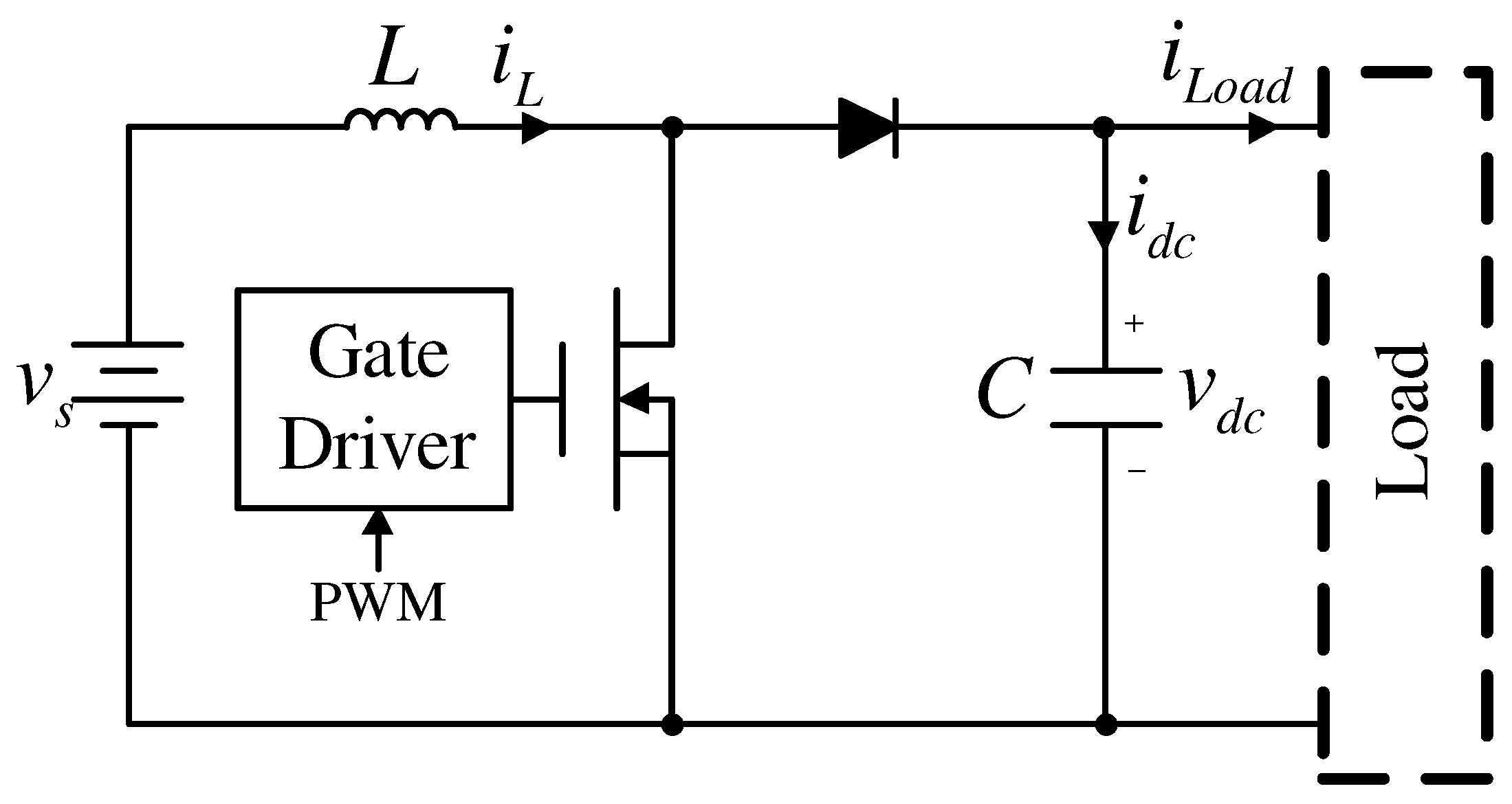
2. Nonlinear Model of DC/DC Boost Converters

Figure 1 shows a DC/DC boost converter circuit with the state variables i L (inductor current in A) and v d c (output voltage in V) driven by a control signal D ( [ 0 , 1 ] , duty ratio) for a given source voltage v s (V) and pulse-width modulation (PWM) period T s , with i L o a d denoting the load current A. The ON/OFF switching actions for each duration time D T s and ( 1 D ) T s yield two different circuits whose average inductor current and output voltage dynamics can be modeled as a bilinear system [5]:
L d i L ( t ) d t = ( 1 u ( t ) ) v d c ( t ) + v s ( t ) ,
C d v d c ( t ) d t = ( 1 u ( t ) ) i L ( t ) i L o a d ( t ) , t 0 ,
with u ( t ) : = D and L and C being the inductance and capacitance values, respectively.
The inductance and capacitance can be affected by considerable variations depending on the operating conditions, which can be written as L = L 0 + Δ L and C = C 0 + Δ C with their known nominal values L 0 and C 0 and the unknown variations Δ L and Δ C . Moreover, to eliminate the input source voltage measurement, consider the expression v s ( t ) = v s , 0 + Δ v s ( t ) , with v s , 0 and Δ v s ( t ) denoting the known initial voltage value and unknown variation, respectively. These notations transform the original inductor current and output voltage dynamics (1) and (2) into a nominal version:
L 0 d i L ( t ) d t = ( 1 u ( t ) ) v d c ( t ) + v s , 0 + w c ( t ) ,
C 0 d v d c ( t ) d t = ( 1 u ( t ) ) i L ( t ) + w v ( t ) , t 0 ,
with unknown time-varying lumped disturbances w c ( t ) and w v ( t ) .
The following section presents the proposed output voltage control law that does not require knowledge of the parameter and load information dependence by using the nominal dynamics (3) and (4) instead of (1) and (2).

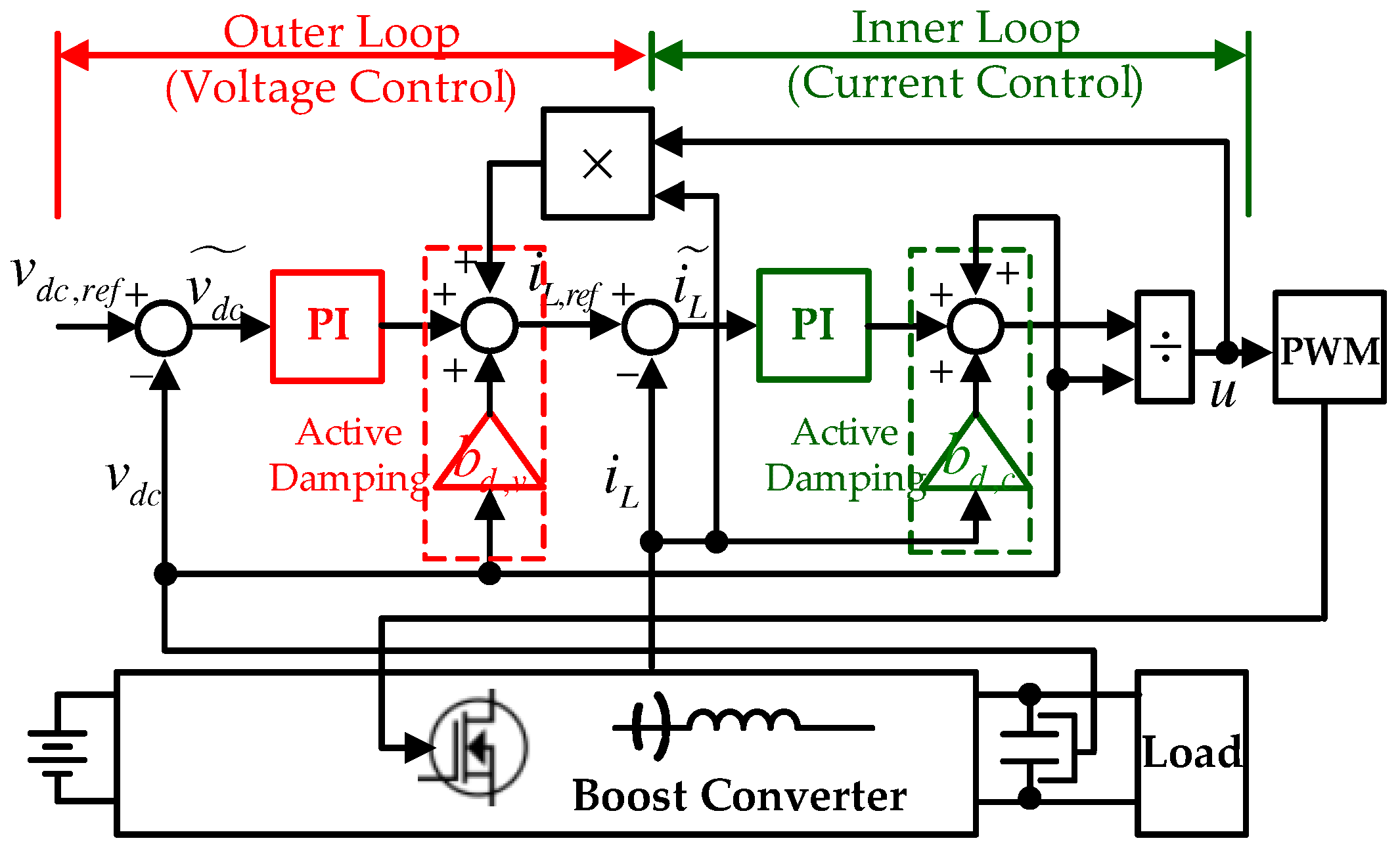
3. Proposed Control Law

3.1. Control Objective

This study attempts to assign the desired transfer functions to the inner and outer loops as
I L ( s ) I L , r e f ( s ) = ω c s + ω c and V d c ( s ) V d c , r e f ( s ) = ω v s + ω v , s C ,
for the reference signals i L , r e f and v d c , r e f (with corresponding Laplace transforms I L , r e f ( s ) and V d c , r e f ( s ) ) and desired outputs i L and v d c (with corresponding Laplace transforms I L ( s ) and V d c ( s ) ) for each loop cut-off frequency, represented as ω c (inner loop, ω c = 2 π f c in rad/s and f c Hz) and ω v (outer loop, ω v = 2 π f v in rad/s and f v Hz). The inverse Laplace transform yields the time-domain expression for (5) as
i ˙ L ( t ) = ω c ( i L , r e f ( t ) i L ( t ) ) , v ˙ v c ( t ) = ω v ( v d c , r e f ( t ) v d c ( t ) ) , t 0 ,
with the notation f ˙ ( t ) : = d f ( t ) d t for any given signal f ( t ) . For this purpose, the control objectives are formulated as exponential convergences:
lim t i L ( t ) = i L ( t ) ,
lim t v d c ( t ) = v d c ( t ) ,
so that the proposed controller constrains the closed-loop inductor current and output voltage dynamics within the desired transfer functions (5).

3.2. Inductor Current Control (Inner Loop)

The proposed current controller for the error i ˜ L ( t ) : = i L , r e f ( t ) i L ( t ) given by
u ( t ) = 1 v d c ( t ) ( b d , c i L ( t ) + L 0 ω c i ˜ L ( t ) + b d , c ω c 0 t i ˜ L ( τ ) d τ ( v s , 0 v d c ( t ) ) ) , t 0 ,
with tuning parameter b d , c > 0 (for active damping) yields the closed-loop current dynamics by substituting it into the open-loop current dynamics (3) such that
L 0 i ˙ L ( t ) = b d , c i L ( t ) + L 0 ω c i ˜ L ( t ) + b d , c ω c 0 t i ˜ L ( τ ) d τ + w c ( t ) , t 0 ,
whose closed-loop behaviors are analyzed in Section 4.
Remark 1.
The proposed control law (9) forces the second-order closed-loop current dynamics (10) to be the first-order low-pass filter (LPF) dynamics through pole-zero cancellation using the active damping term b d , c i L ( t ) and the PI gain setting to guarantee the control objective (7). Moreover, the active damping coefficient b d , c determines the current-loop disturbance attenuation level including the transient periods. Section 4 presents the formal analysis.

3.3. Output Voltage Control (Outer Loop)

The output voltage dynamics (4) gives its another expression by adopting i ˜ L ( t ) = i L , r e f ( t ) i L ( t ) as
C 0 v ˙ d c ( t ) = i L ( t ) u ( t ) i L ( t ) + w v ( t ) = i L , r e f ( t ) i ˜ L ( t ) u ( t ) i L ( t ) + w v ( t ) , t 0 ,
whose stabilization can be accomplished by the proposed output voltage controller for the error v ˜ d c ( t ) : = v d c , r e f ( t ) v d c ( t ) such that
i L , r e f ( t ) = b d , v v d c ( t ) + C 0 ω v v ˜ d c ( t ) + b d , v ω v 0 t v ˜ d c ( τ ) d τ + u ( t ) i L ( t ) , t 0 ,
with tuning parameter b d , v > 0 (for active damping). The control law (12) gives the closed-loop output voltage dynamics by substituting it to the open-loop output voltage dynamics (11) such that
C 0 v ˙ d c ( t ) = b d , v v d c ( t ) + C 0 ω v v ˜ d c ( t ) + b d , v ω v 0 t v ˜ d c ( τ ) d τ i ˜ L ( t ) + w v ( t ) , t 0 ,
whose closed-loop behaviors are analyzed in Section 4.
Remark 2.
The proposed control law (12) reduces the closed-loop second-order dynamics to the first-order LPF dynamics by injecting the pole and zero into the same location (leading to pole-zero cancellation) using the active damping b d , v v d c ( t ) and appropriate PI gain setting that guarantee the control objective (8). Moreover, the active damping coefficient b d , v determines the voltage-loop disturbance attenuation level including the transient periods. Section 4 presents the formal analysis.
Remark 3.
There are four design parameters as (for inner loop) b d , c , ω c , (for outer loop) b d , v , and ω v whose recommended tuning process is given as follows.
1. 
(inner loop) Setting b d , c = 0 , increase f c (leading to ω c = 2 π f c ) until an acceptable proportional inductor current control performance is achieved (normal range: 10 f c 200 Hz).
2. 
For a chosen f c from the previous step, increase b d , c from zero until the controlled inductor current trajectory i L is close to its desired trajectory i L as possible.
3. 
(outer loop) Setting b d , v = 0 , increase f v (leading to ω v = 2 π f v ) until an acceptable proportional output voltage control performance is achieved (normal range: f v 0.1 f c Hz).
4. 
For a chosen f v from the previous step, increase b d , v from zero until the controlled output voltage trajectory v d c is close to its desired trajectory v d c as possible.
This process gives the design parameter tuning result used in Section 5.
Figure 2 presents the closed-loop cascade system structure using the proposed inner and outer loop controllers (9) and (12) as the main topic of this section.

4. Analysis

This section presents the closed-loop analysis, proving that the proposed cascade system shown in Figure 2 accomplishes the control objectives (7) and (8) and provides a rough design parameter selection guideline. To this end, Section 4.1 analyzes the inner loop current control system, the results of which are used as the basis to prove the control objective accomplishment.

4.1. Inductor Current Control Loop

Lemma 1 presents an interesting result related to the closed-loop order reduction caused by active damping and the PI gain setting in the inductor current control action (9).
Lemma 1.
The controlled inductor current in the cascade system depicted in Figure 2 satisfies
i ˙ L ( t ) = ω c ( i L , r e f ( t ) i L ( t ) ) + f c , F ( t ) ,
with the auxiliary system
f ˙ c , F ( t ) = b d , c L 0 f c , F ( t ) + 1 L 0 f c ( t ) , t 0 ,
and the input signal f c ( t ) : = Δ w ˙ c ( t ) depending on the AC component of the disturbance w c ( t ) (e.g., w c ( t ) = w c , 0 ( D C c o m p o n e n t ) + Δ w c ( t ) (AC component)).
Proof. 
The definition of ζ c : = b d , c ω c 0 t i ˜ L d τ gives a two-dimensional state-space representation for the closed-loop inductor current dynamics (10) such that
x ˙ c = A c x c + b c i L , r e f + b c , w w c , y c = c c x c , t 0 ,
where x c : = i L ζ c , A c : = b d , c + L 0 ω c L 0 1 L 0 b d , c ω c 0 , b c : = ω c b d , c ω c , b c , w : = 1 L 0 0 , and c c : = 1 0 . The Laplace transform of this state-space representation results in
Y c ( s ) = c c ( s I A c ) 1 b c I L , r e f ( s ) + c c ( s I A c ) 1 b c , w W c ( s ) , s C ,
which yields the relationships:
c c ( s I A c ) 1 b c = ω c ( L 0 s + b d , c ) ( s + ω c ) ( L 0 s + b d , c ) = ω c s + ω c , c c ( s I A c ) 1 b c , w = s ( s + ω c ) ( L 0 s + b d , c ) , s C ,
where the order reduction (through pole-zero cancellation) occurs in the first result above from the combination of the active damping term and the PI gain setting. These two results lead to
( s + ω c ) Y c ( s ) = ω c I L , r e f ( s ) + F c ( s ) , s C ,
where F c ( s ) = 1 L 0 s + b d , c s W c ( s ) , which completes the proof. □
The controlled inductor current dynamics (14) and (15) as the result of Lemma 1 play an important role in deriving the exponential convergence with respect to the error defined as e L ( t ) : = i L ( t ) i L ( t ) , which is presented in Theorem 1 in detail.
Theorem 1.
The controlled inductor current from the cascade system depicted in Figure 2 satisfies
e L ( t ) a c , 1 e a c , 2 t , t 0 , | f c , F ( t ) | 2 f c , m a x b d , c
for some a c , i > 0 , i = 1 , 2 , where e L ( t ) = i L ( t ) i L ( t ) and | f c ( t ) | f c , m a x , t 0 .
Proof. 
It follows from (6), (14), and e L = i L i L that
e ˙ L = ω c e L f c , F , t 0 ,
which leads to the time derivative of the Lyapunov function candidate V c : = 1 2 x c P c x c with x c : = e L f c , F T and P c : = diag { 1 , L 0 } as
V ˙ c = e L ( ω c e L f c , F ) + f c , F ( b d , c f c , F + f c ) = x c Q c x c f c , F ( b d , c 2 f c , F f c ) α c V c , t 0 , | f c , F | 2 f c , m a x b d , c ,
with | f c | f c , m a x , t 0 , α c : = 2 λ m i n ( Q c ) λ m a x ( P c ) , positive definite matrix Q c : = ω c 1 0 b d , c 2 , and λ m i n ( ( · ) ) and λ m a x ( ( · ) ) being the minimum and maximum eigenvalues of any square matrix ( · ) , respectively. This completes the proof by using the comparison principle in [24]. □
For the reminder of the analysis, it is assumed that 2 f c , m a x b d , c 0 for a sufficiently large choice of b d , c > 0 such that
V ˙ c ( x c ( t ) ) α c V c ( x c ( t ) ) , t 0 ,
(obtained from (17)), which roughly defines the exponential convergence
lim t i L ( t ) = i L ( t ) ,
and thus, the control objective (7) is accomplished using the proposed inner loop current controller. Moreover, the inequality (18) simplifies the proof process to prove the exponential convergence of the original inductor current error i ˜ L ( t ) = i L , r e f ( t ) i L ( t ) .
Theorem 2.
The controlled inductor current in the cascade system depicted in Figure 2 satisfies
i ˜ L ( t ) b 1 e b 2 t , t 0 , | i ˜ L ( t ) | 2 δ ω c ,
for some b i > 0 , i = 1 , 2 , where | i ˙ L , r e f ( t ) | δ , t 0 .
Proof. 
The error i ˜ L = i L , r e f i L gives its dynamics from (10) as
i ˜ ˙ L = ω c i ˜ L f c , F + i ˙ L , r e f , t 0 ,
which leads to the time derivative of the composite-type Lyapunov function candidate V c : = 1 2 i ˜ L 2 + η V c with η > 0 as
V ˙ c = i ˜ L ( ω c 2 i ˜ L f c , F ) i ˜ L ( ω c 2 i ˜ L i ˙ L , r e f ) + η V ˙ c ω c 4 i ˜ L 2 ( η α c 1 L 0 ω c ) V c , t 0 , | i ˜ L | 2 δ ω c ,
with | i ˙ L , r e f | δ , t 0 , where the Young’s inequality x y ϵ 2 x 2 + 1 2 ϵ y 2 , ϵ > 0 and inequality (18) verify the inequality above. The upper bound of V ˙ c can be obtained by setting η : = 1 α c ( 1 L 0 ω c + 1 ) as
V ˙ c ω c 4 i ˜ L 2 V c α c V c , t 0 , | i ˜ L | 2 δ ω c ,
with α c : = min { ω c 2 , 1 η } , which completes the proof using the comparison principle in [24]. □
For the reminder of the analysis, it is assumed that 2 δ ω c 0 for a sufficiently large choice of ω c > 0 such that
V ˙ c ( i ˜ L ( t ) , x c ( t ) ) α c V c ( i ˜ L ( t ) , x c ( t ) ) , t 0 ,
which is used as a useful result for proving the control objective accomplishment (8) in Theorem 3 (the main result of this section).

4.2. Output Voltage Control Loop

Lemma 2 presents an interesting result related to the closed-loop order reduction caused by active damping and the PI gain setting in the output voltage control action (12).
Lemma 2.
The controlled output voltage from the cascade system depicted in Figure 2 satisfies
v ˙ d c ( t ) = ω v ( v d c , r e f ( t ) v d c ( t ) ) κ 1 i ˜ L ( t ) + i ˜ L , F ( t ) + f v , F ( t ) ,
with the auxiliary systems
i ˜ ˙ L , F ( t ) = κ 2 i ˜ L , F ( t ) + κ 3 i ˜ L ( t ) ,
f ˙ v , F ( t ) = b d , v C 0 f v , F ( t ) + 1 C 0 f v ( t ) , t 0 ,
for some κ i > 0 , i = 1 , 2 , 3 , and the input signal f v ( t ) : = Δ w ˙ v ( t ) and Δ w v ( t ) depending on the AC component of the disturbance w v ( t ) (e.g., w v ( t ) = w v , 0 ( D C c o m p o n e n t ) + Δ w v ( t ) (AC component)).
Proof. 
The definition of ζ v : = b d , v ω v 0 t v ˜ d c d τ gives a two-dimensional state-space representation for the closed-loop output voltage dynamics (13) as
x ˙ v = A v x v + b v v d c , r e f + b v , w ( i ˜ L + w v ) , y v = c v x v , t 0 ,
where x v : = v d c ζ v , A v : = b d , v + C 0 ω v C 0 1 C 0 b d , v ω v 0 , b v : = ω v b d , v ω v , b v , w : = 1 C 0 0 , and c v : = 1 0 . The Laplace transform for this state space representation results in
Y v ( s ) = c v ( s I A v ) 1 b v V d c , r e f ( s ) + c v ( s I A v ) 1 b v , w ( I ˜ L ( s ) + W v ( s ) ) , s C ,
which in turn yields the relationships:
c v ( s I A v ) 1 b v = ω v ( C 0 s + b d , v ) ( s + ω v ) ( C 0 s + b d , v ) = ω v s + ω v , c v ( s I A v ) 1 b v , w = s ( s + ω v ) ( C 0 s + b d , v ) , s C ,
where the order reduction (by pole-zero cancellation) occurs in the first result above from the combination of the active damping term and the PI gain setting. These two results with the relationships s C 0 s + b d , v = κ 1 κ 3 s + κ 2 , κ 1 : = 1 C 0 , κ 2 : = b d , v C 0 , and κ 3 : = b d , v C 0 2 lead to
( s + ω v ) Y v ( s ) = ω v V d c , r e f ( s ) κ 1 I ˜ L ( s ) + I ˜ L , F ( s ) + F v ( s ) , s C ,
where I ˜ L , F ( s ) = κ 3 s + κ 2 I ˜ L ( s ) and F v ( s ) = 1 C 0 s + b d , v s W v ( s ) , which completes the proof. □
The controlled output dynamics (22) and (23) as the result of Lemma 2 play an important role in deriving the exponential convergence with respect to the error (defined as e v ( t ) : = v d c ( t ) v d c ( t ) ), which is presented in Theorem 3 in detail.
Theorem 3.
The controlled output voltage in the cascade system shown in Figure 2 satisfies
e v ( t ) a v , 1 e a v , 2 t , t 0 , | f v , F ( t ) | 2 f v , m a x b d , v
for some a v , i > 0 , i = 1 , 2 , where e v ( t ) = v d c ( t ) v d c ( t ) and | f v ( t ) | f v , m a x , t 0 .
Proof. 
It follows from (6), (22), and e v = v d c v d c that
e ˙ v = ω v e v i ˜ L , F + κ 1 i ˜ L f v , F , t 0 ,
which leads to the time derivative of the composite-type Lyapunov function candidate V v : = 1 2 x v P v x v + ρ V c with ρ > 0 and x v : = e v i ˜ L , F i ˜ L f v , F T and P v : = d i a g { 1 , 1 , 1 , C 0 } as
V ˙ v = e v ( ω v e v i ˜ L , F + κ 1 i ˜ L f v , F ) + i ˜ L , F ( κ 2 i ˜ L , F + κ 3 i ˜ L ) + i ˜ L ( ω c i ˜ L f c , F + i ˙ L , r e f ) + f v , F ( b d , v f v , F + f v ) + ρ V ˙ c x v Q v x v ( ρ α c 2 η L 0 ω c ) V c f v , F ( b d , v 2 f v , F f v ) , t 0 , | i ˜ L | 2 δ ω c .
Setting ρ : = 1 α c ( 2 η L 0 ω c + 1 ) and 2 δ ω c 0 results in
V ˙ v α v V v , t 0 , | f v , F | 2 f v , m a x b d , v ,
with α v : = min { 2 λ m i n ( Q v ) λ m a x ( P v ) , 1 ρ } , positive definite matrix Q v : = ω v 1 κ 1 1 0 κ 2 κ 3 0 0 0 ω c 4 0 0 0 0 b d , v 2 , and | f v | f v , m a x , t 0 . This completes the proof by using the comparison principle in [24]. □
The inequality (25) as the main result of this section concludes that the proposed control law comprising (9) and (12) ensures the exponential convergence (control objective (8)):
lim t v d c ( t ) = v d c ( t ) , lim t i L ( t ) = i L ( t ) ,
subject to the design parameter setting guideline given by 2 f c , m a x b d , c 0 , 2 f v , m a x b d , v 0 (for active damping coefficients) and by 2 δ ω c 0 (for the current cut-off frequency).

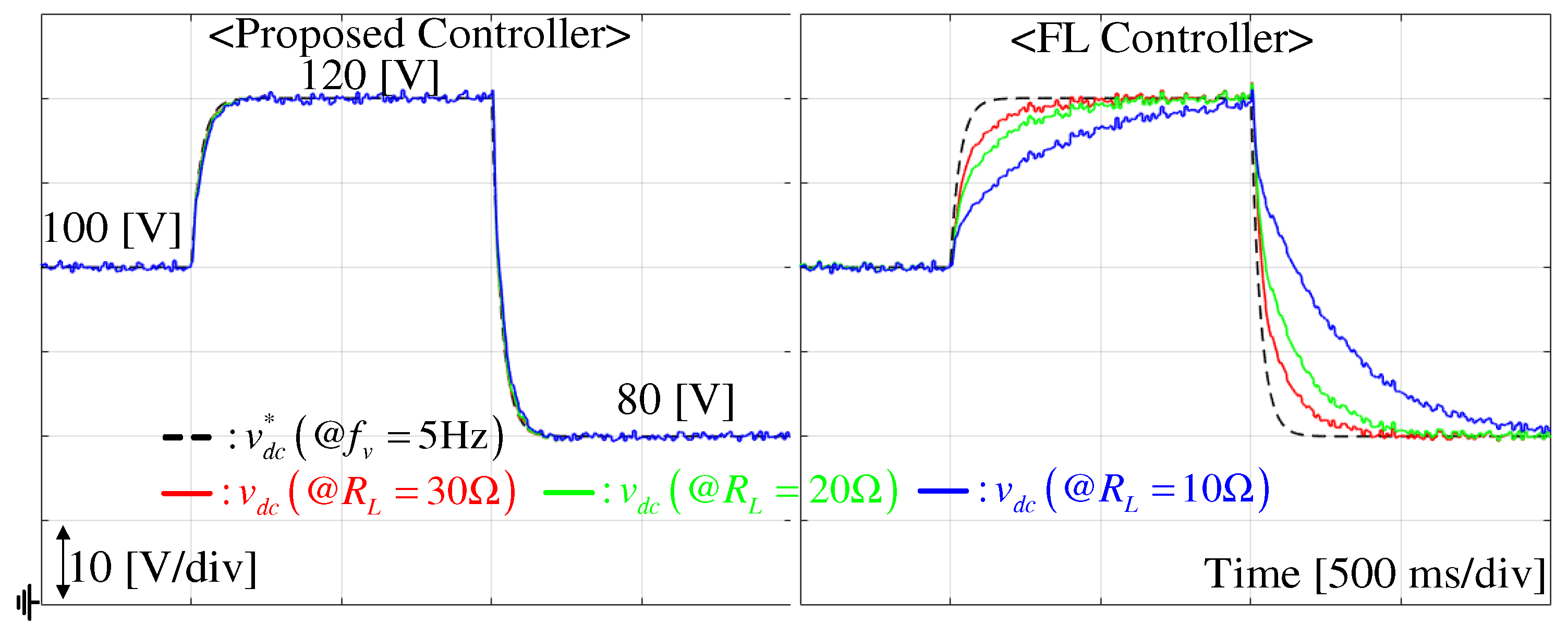
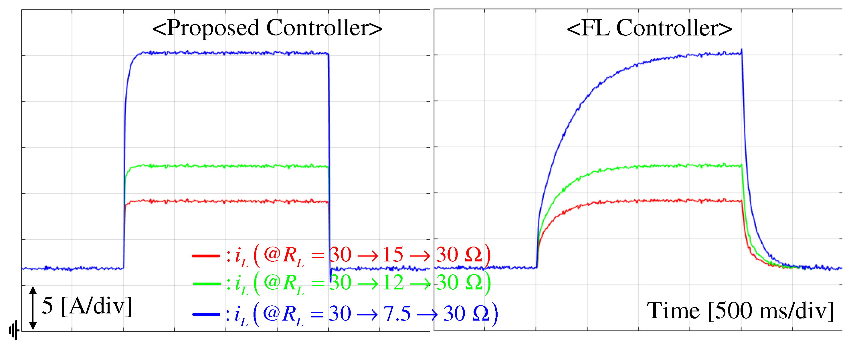
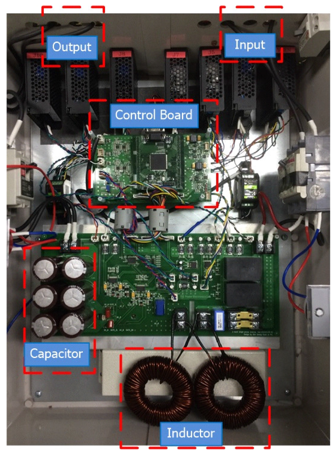
5. Experimental Results

This section uses the DC/DC boost converter depicted in Figure 3 to exhibit the closed-loop improvement accomplished by the proposed technique; the identified inductance and capacitance values are L = 2 mH and C = 2500 μF, respectively. A 50 V battery was used as the input source voltage v s , and a resistive load R L = 30 Ω was initially connected to the converter output port. The control and sampling periods were set to be 0.1 ms with the switching frequency 10 kHz to implement the control algorithm using a Texas Instruments 32-bit processor (DSP28335). The control algorithm was coded using the C program and the nominal converter parameter value setting L 0 = 0.7 L and C 0 = 0.8 C ; this choice was considered to clarify the closed-loop performance improvement by the active damping terms depressing the magnified disturbances. Note that it is desirable to choose the identified inductance and capacitance values by the manufacture as the nominal values used for the controller implementation in the actual applications.
The inner and outer loops for the proposed cascade system were set as follows: (inner loop) f c = 100 Hz for ω c = 2 π 100 rad/s, b d , c = 5 , (outer loop) f v = 5 Hz for ω v = 2 π 5 rad/s, and b d , v = 0.5 . A cascade-type PI controller including a feed-forward compensation term (introduced in [5] and called the FL controller) was used for comparison purposes which is given by
  • (Inner Loop)
    u ( t ) = 1 v d c ( t ) ( 2 L 0 ω c i ˜ L ( t ) + L 0 ω c 2 0 t i ˜ L ( τ ) d τ ( v s , 0 v d c ( t ) ) ) ,
  • (Outer Loop)
    i L , r e f ( t ) = 2 C 0 ω v v ˜ d c ( t ) + C 0 ω v 2 0 t v ˜ d c ( τ ) d τ , t 0 ,
    whose PI gains were designed for the inner and outer loop cut-off frequencies at ω c ( = 2 π 100 rad / s ) and ω v ( = 2 π 5 rad / s ) , respectively. The following subsections compare the proposed and FL controllers in both the qualitative and quantitative manners using the performance metric J : = 0 | v d c , r e f ( t ) v d c ( t ) | 2 d t .

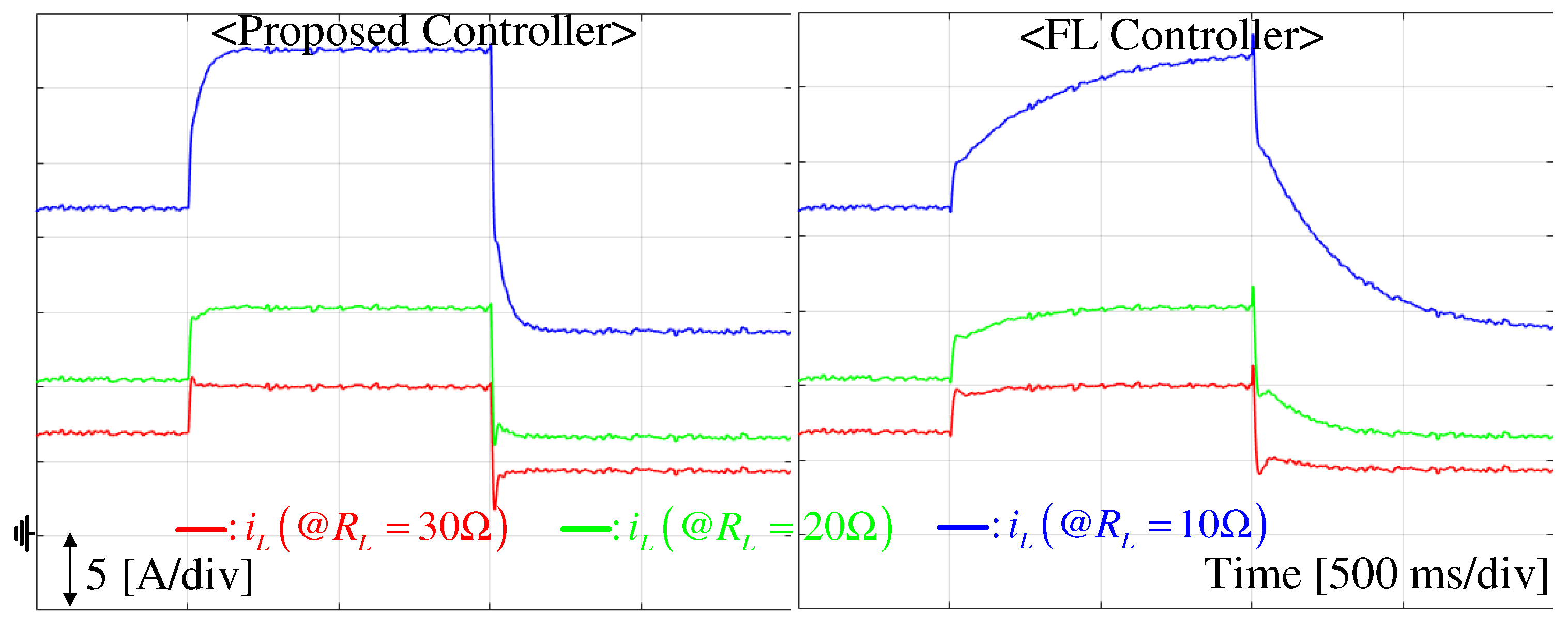
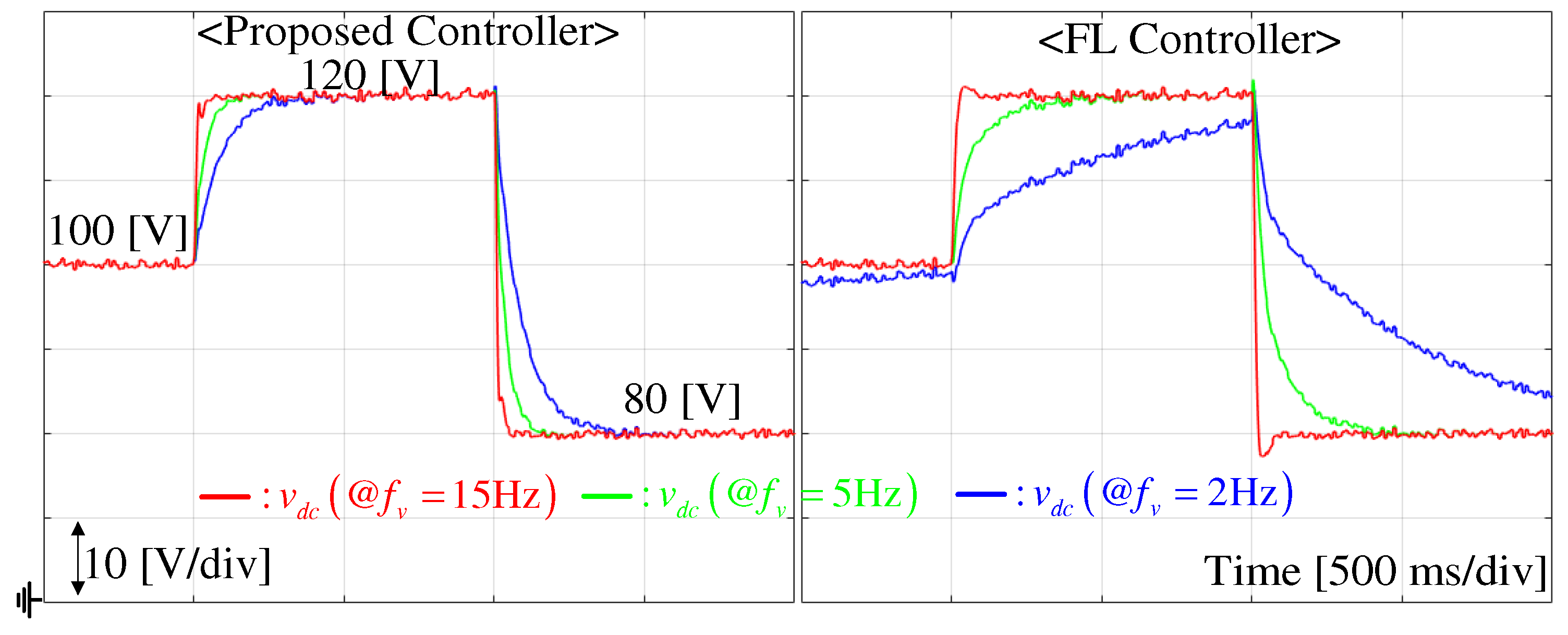
5.1. Pulse Reference Tracking Performance Comparison

This experiment aims to show the constant reference tracking performance improvement of the proposed controller using three resistive loads R L = 30 , 20 , 10 Ω . The initial output voltage reference v d c , r e f = 100 V was suddenly increased to 120 V and then decreased to 80 V sequentially. Figure 4 clearly demonstrates the superiority of the proposed controller depressing the tracking performance variations compared to the FL controller; the active damping injection and suggested PI gain setting led to this significant advantage by exploiting the useful closed-loop properties discussed in Section 4. The closed-loop inductor current responses during operation are presented in Figure 5, indicating considerably faster current dynamics using the proposed controller (incorporating tolerable overshoots) compared to the FL controller.

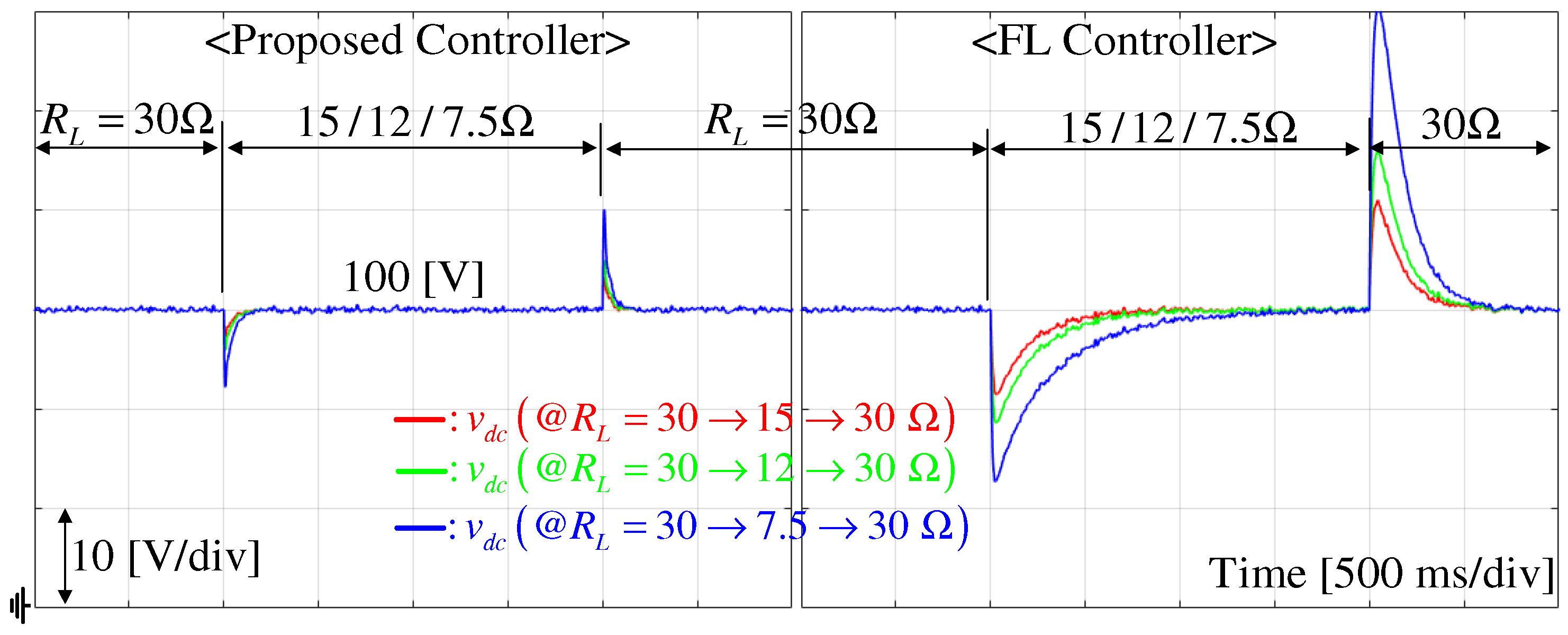
5.2. Constant Reference Regulation Performance Comparison

This subsection compares the closed-loop performance at a fixed v d c , r e f = 50 V under three decreasing resistive load variations ( R L = 15 / 12 / 7 Ω ) with respect to restoring the load to its initial value of R L = 30 Ω in a sequential and abrupt manner. As presented in Figure 6, the proposed controller accomplishes a significant performance improvement from two perspectives: the over/undershoot level reduction and performance inconsistencies caused by the different operating conditions. The pole-zero cancellation technique based on active damping injection resulted in this practical improvement. Rapid current responses under the three load variation scenarios were also obtained using the proposed control scheme, as shown in Figure 7.
Table 1 presents the numerical performance comparison results under the output voltage tracking (Section 5.1) and regulation (Section 5.2) tasks using the performance metric J = 0 | v d c , r e f ( t ) v d c ( t ) | 2 d t . From this result, the proposed controller achieved the significant closed-loop performance improvement at least two times compared with the FL controller.

5.3. Pulse Reference Performance Variation Comparison

This subsection verifies the nature of the performance recovery proven in Theorem 3, which is considered to be the main result of this study. For this purpose, three output voltage cut-off frequencies f v = 2 , 5 , 15 Hz were applied to the closed-loop with a fixed current cut-off frequency defined as f c = 100 Hz, a load R L = 30 Ω , and the pulse output voltage reference used in Section 5.1. Figure 8 presents the comparison results, in which the proposed technique successfully assigns the desired output voltage cut-off frequency to the closed-loop system by exploiting the beneficial property described by Theorem 3.

6. Conclusions

This study suggests an improved cascade-type output voltage regulator by considering two features: active damping injection and a suitable PI gain structure for both the inner and outer loops. Beneficial closed-loop convergences were proven through closed-loop analysis, which included a rough design parameter tuning guideline, and revealed interesting features such as pole-zero cancellation and performance recovery. An experimental study demonstrated the practical merits of the proposed controller, demonstrating considerable improvements in closed-loop performance.

Author Contributions

Conceptualization and methodology, S.-K.K.; software, validation, formal analysis, investigation, writing—original draft preparation, and writing—review and editing, S.H.Y. and K.B.; resources, supervision, project administration, and funding acquisition, D.S.K. All authors have read and agreed to the published version of the manuscript.

Funding

This research was supported in part by the National Research Foundation of Korea (NRF) grant funded by the Korea government (Ministry of Science and ICT) (No. NRF-2021R1C1C1004380) and was supported in part by the Basic Science Research Program through the National Research Foundation of Korea (NRF) funded by the Ministry of Education (2018R1A6A1A03026005).

Conflicts of Interest

The authors declare no conflict of interest.

References

  1. Choi, K.; Kim, D.; Kim, S.K. Disturbance Observer-Based Offset-Free Global Tracking Control for Input-Constrained LTI Systems with DC/DC Buck Converter Applications. Energies 2020, 13, 4079. [Google Scholar] [CrossRef]
  2. Chen, Y.C.; Chen, L.R.; Lai, C.M.; Lin, Y.C.; Kuo, T.J. Development of a DC-Side Direct Current Controlled Active Ripple Filter for Eliminating the Double-Line-Frequency Current Ripple in a Single-Phase DC/AC Conversion System. Energies 2020, 13, 4772. [Google Scholar] [CrossRef]
  3. Li, J.; Tang, J.; Wang, X.; Xiong, B.; Zhan, S.; Zhao, Z.; Hou, H.; Qi, W.; Li, Z. Optimal Placement of IoT-Based Fault Indicator to Shorten Outage Time in Integrated Cyber-Physical Medium-Voltage Distribution Network. Energies 2020, 13, 4928. [Google Scholar] [CrossRef]
  4. Silva, F.; Carvalho, P.; Ferreira, L. Improving PV Resilience by Dynamic Reconfiguration in Distribution Grids: Problem Complexity and Computation Requirements. Energies 2021, 14, 830. [Google Scholar] [CrossRef]
  5. Erickson, R.W.; Maksimovic, D. Fundamentals of Power Electronics, 2nd ed.; Springer: New York, NY, USA, 2001. [Google Scholar]
  6. Kapat, S.; Patra, A. A Current-Controlled Tristate Boost Converter with Improved Performance Through RHP Zero Elimination. IEEE Trans. Power Electron. 2009, 24, 776–786. [Google Scholar] [CrossRef]
  7. Alexander, G.P.; Feng, G.; Yan-Fei, L.; Paresh, C.S. A Design Method for PI-like Fuzzy Logic Controllers for DC/DC Converter. IEEE Trans. Ind. Electron. 2007, 54, 2688–2696. [Google Scholar]
  8. Kapat, S.; Krein, P.T. Formulation of PID Control for DC-DC Converters Based on Capacitor Current: A Geometric Context. IEEE Trans. Power Electron. 2012, 27, 1424–1432. [Google Scholar] [CrossRef]
  9. Kazmierkowski, M.P.; Krishnan, R.; Blaabjerg, F. Control in Power Electronics—Selected Problems; Academic Press: Cambridge, MA, USA, 2002. [Google Scholar]
  10. Bibian, S.; Jin, H. High Performance Predictive Dead-Beat Digital Controller for DC Power Supplies. IEEE Trans. Power Electron. 2002, 17, 420–427. [Google Scholar] [CrossRef]
  11. Zhang, Q.; Min, R.; Tong, Q.; Zou, X.; Liu, Z.; Shen, A. Sensorless Predictive Current Controlled DC-DC Converter With a Self-Correction Differential Current Observer. IEEE Trans. Ind. Electron. 2014, 61, 6747–6757. [Google Scholar] [CrossRef]
  12. Oucheriah, S.; Guo, L. PWM-Based Adaptive Sliding-Mode Control for Boost DC/DC Converters. IEEE Trans. Ind. Electron. 2013, 60, 3291–3294. [Google Scholar] [CrossRef]
  13. Wang, Y.X.; Yu, D.H.; Kim, Y.B. Robust Time-Delay Control for the DC/DC Boost Converter. IEEE Trans. Ind. Electron. 2014, 61, 4829–4837. [Google Scholar] [CrossRef]
  14. He, J.; Zhang, X. An Ellipse-Optimized Composite Backstepping Control Strategy for a Point-of-Load Inverter Under Load Disturbance in the Shipboard Power System. IEEE Open J. Power Electron. 2020, 1, 420–430. [Google Scholar] [CrossRef]
  15. Hassan, M.A.; Li, E.; Li, X.; Li, T.; Duan, C.; Chi, S. Adaptive Passivity-Based Control of DC-DC Buck Power Converter With Constant Power Load in DC Microgrid Systems. IEEE J. Sel. Top. Power Electron. 2019, 7, 2029–2040. [Google Scholar] [CrossRef]
  16. Kim, S.-K.; Lee, K.-B. Robust Feedback-Linearizing Output Voltage Regulator for DC/DC Boost Converter. IEEE Trans. Ind. Electron. 2015, 62, 7127–7135. [Google Scholar] [CrossRef]
  17. Theunisse, T.A.F.; Chai, J.; Sanfelice, R.G.; Heemels, W.P.M.H. Robust Global Stabilization of the DC-DC Boost Converter via Hybrid Control. IEEE Trans. Circuits Syst. I Regul. Pap. 2015, 62, 1052–1061. [Google Scholar] [CrossRef] [Green Version]
  18. Yang, J.; Wu, B.; Li, S.; Yu, X. Design and Qualitative Robustness Analysis of an DOBC Approach for DC-DC Buck Converters With Unmatched Circuit Parameter Perturbations. IEEE Trans. Circuits Syst. I Regul. Pap. 2016, 63, 551–560. [Google Scholar] [CrossRef]
  19. Xu, Q.; Zhang, C.; Wen, C.; Wang, P. A Novel Composite Nonlinear Controller for Stabilization of Constant Power Load in DC Microgrid. IEEE Trans. Smart Grid 2019, 10, 752–761. [Google Scholar] [CrossRef]
  20. Kim, S.-K. Output Voltage-Tracking Controller with Performance Recovery Property for DC/DC Boost Converters. IEEE Trans. Control Syst. Technol. 2018, 27, 1301–1307. [Google Scholar] [CrossRef]
  21. Kim, S.-K.; Ahn, C.K. Nonlinear Tracking Controller for DC/DC Boost Converter Voltage Control Applications via Energy-Shaping and Invariant Dynamic Surface Approach. IEEE Trans. Circuits Syst. II Express Briefs 2019, 66, 1855–1859. [Google Scholar] [CrossRef]
  22. Kim, S.-K.; Kim, K.-C.; Ahn, C.K. Output-voltage-tracking Control for Buck Converters using Variable Convergence Rate Mechanism without Current Feedback. IEEE Trans. Ind. Electron. 2021, in press. [Google Scholar] [CrossRef]
  23. Lee, K.; Lee, J.; Lee, Y.I. Robust Model Predictive Speed Control of Induction Motors Using a Constrained Disturbance Observer. Int. J. Control Autom. Syst. 2020, 18, 1539–1549. [Google Scholar] [CrossRef]
  24. Khalil, H.K. Nonlinear Systems; Prentice Hall: Upper Saddle River, NJ, USA, 2002. [Google Scholar]
Figure 1. Circuit configuration of DC/DC boost converters.
Energies 14 03824 g001
Figure 2. Proposed cascade-type output voltage control system.
Energies 14 03824 g002
Figure 3. 3-kW DC/DC boost converter hardware configuration.
Energies 14 03824 g003
Figure 4. Controlled output voltage responses under pulse reference tracking task for resistive loads R L = 30 , 20 , 10 Ω .
Energies 14 03824 g004
Figure 5. Controlled inductor current responses under pulse reference tracking task for resistive loads R L = 30 , 20 , 10 Ω .
Energies 14 03824 g005
Figure 6. Controlled output voltage responses under constant reference regulation task with respect to abrupt resistive load variations: R L = 30 15 / 12 / 7.5 30 Ω .
Energies 14 03824 g006
Figure 7. Controlled output voltage responses under constant reference regulation task with respect to abrupt resistive load variations: R L = 30 15 / 12 / 7.5 30 Ω .
Energies 14 03824 g007
Figure 8. Controlled output voltage performance under fixed resistive load R L = 30   Ω and increasing output voltage cut-off frequency: f v = 2 , 5 , 15 Hz.
Energies 14 03824 g008
Table 1. Numerical performance comparison results under tracking and regulation tasks using performance metric J.
Energies 14 03824 i001
Publisher’s Note: MDPI stays neutral with regard to jurisdictional claims in published maps and institutional affiliations.

