Article

Voltage-Gain Design and Efficiency Optimization of Series/Series-Parallel Inductive Power Transfer System Considering Misalignment Issue

1
Department of Electrical Engineering, Shenyang University of Technology, Shenyang 110870, China
2
Clean Energy Development Institute of State Grid Qinghai Electric Power Company, Xining 810008, China
*
Author to whom correspondence should be addressed.
Energies 2021, 14(11), 2999; https://doi.org/10.3390/en14112999
Submission received: 14 March 2021 / Revised: 8 April 2021 / Accepted: 19 April 2021 / Published: 21 May 2021

Abstract

:
Compensation is key to an inductive power transfer (IPT) system in terms of voltage transfer function and efficiency optimization. Basic compensation is simple, but not suitable, for the achievement of variable load-independent voltage-gains without changing the design of the loosely-coupled transformer (LCT). On the other hand, higher-order compensation circuits enable greater design freedom to achieve variable load-independent voltage-gains while keeping the LCT unchanged, but it requires a variety of compensation components, especially the inductive components, which incur significant copper and core losses. This paper proposes a comprehensive design of the series/series-parallel (S/SP) IPT system. The design methodology for variable load-independent voltage-gains is studied to keep the LCT unchanged and achieve zero phase angle input over the whole load range. Design consideration includes the effect of misalignment issue on the voltage-gain and, thus, a design criteria can be derived to ensure an acceptable sensitivity to the misalignment when taking efficiency optimization. The experimental results are presented for verification.

1. Introduction

Inductive power transfer (IPT) technology enables wireless power delivery over an air gap distance via magnetic field coupling. Because of the elimination of physical contact, IPT has shown great potential in cutting electric cables in a variety of power delivery scenarios, such as consumer electronics [1], biomedical implants [2], industrial electronics [3], electric vehicles [4,5], and so on. When compared with traditional conductive power transfer, the benefits of IPT charging include high reliability in hazardous environments, friendly user-experience, and low maintenance cost [6].
As the key component in IPT, the loosely coupled transformer (LCT) is formed by the transmitter coil in the primary and the receiver coil in the secondary. Large leakage magnetic field cannot be avoided in the LCT [7]. Thus, using reactive components for compensation is necessary to ensure effective power delivery in the IPT system [8]. When we design the compensation circuit, load-independent output and zero phase angle (ZPA) input are usually desired for eliminating the control effect and maximizing voltage-ampere rating, respectively. Moreover, as the LCT us usually constrained by its parameters duet to fixed structure and limited space, variable voltage-gains by compensation design should also be taken into consideration to meet specific requirements in some application scenarios [9]. As an example, according to wireless electric vehicle charging standard SAE J 2954 TM , a coil and winding geometry specification is suggested, but the bus voltage on vehicle side may differ in level, depending on specifications of the batteries or supercapacitors, which poses challenges in achieving variable voltage-gains without redesigning the LCT [10,11]. Therefore, it is worth optimizing the compensation design for variable voltage-gains against the constraints of LCT parameters. In addition, the misalignment issue is another factor that frequently causes parameter variation in the LCT, such that compensation design should be evaluated under misalignment issues.
Only using minimum number of external capacitive components, i.e., two capacitors, basic compensation circuits are usually adopted. There includes no external inductive components and, thus, copper and core losses can be avoided in the compensation circuits [12]. Based on the ways of connection, there are totally four basic compensation circuits, which are named series/series (SS), series/parallel (SP), parallel/series, and parallel/parallel [12], as shown in Figure 1. The four basic compensation circuits have been widely studied, and it is found that their output to input transfer functions greatly rely on LCT parameters. For example, the load-independent current transfer function of the SS IPT system and load-independent voltage transfer function of the SP IPT system are typically i o v i 1 ω k L P L S and v o v i 1 k L S L P , respectively [13,14], and it can be observed that they are solely dependent on parameters of the LCT. Once the LCT is designed, the system transfer functions are almost fixed unless a new LCT is used. To address the problems above, more reactive components for compensation are needed, which usually include inductors. Higher-order compensation circuits have more design freedom for output transfer functions without the necessity of redesigning the LCT [15]. For examples, LC/LC compensation [16] and LCC/LCC compensation [17]. By changing the compensation parameters, variable load-independent current or/and voltage transfer functions with ZPA input can be achieved, regardless of the load conditions. Normally, a general method is adopted to do so [9,18,19]. However, the efficiency will be degraded by the additional inductors with significant copper and core losses, which is a major concern of these higher-order compensation circuits. Therefore, either the basic or higher-order compensation circuits have drawbacks, which motivates us to study the series/series-parallel compensation circuit presented in this paper.
The series/series-parallel (S/SP) compensation circuit has no lossy inductive components, as shown by Figure 2. It is also relatively easy to implement variable load-independent voltage-gains output and ZPA input. Thus, it can be considered as a trade-off between basic compensation and higher-order compensation. The primary leakage inductance L l , P , secondary leakage inductance L l , S , and mutual inductance L M of the T-circuit model of the LCT are fully compensated by C P , C S , and C S , P , respectively, such that the S/SP IPT system can behave as an ideal LCT with a turn ratio of 1 n to achieve load-independent voltage-gain and ZPA input [20,21,22]. This intuitive design concept fixes the LIV transfer function at a k-independent point featuring misalignment-tolerance, but it does not meet the desired requirement of variable voltage-gains. Moreover, the efficiency performance and effect of misalignment is not discussed under different designs of compensation parameters. Thus, it motivates us to further investigate the compensation design of the S/SP IPT converter.
This paper elaborates a compensation design to achieve variable load-independent voltage-gains with ZPA input. When compared with the conventional design, the proposed design methodology enables the customization of the voltage gain with the elimination of redesigning the LCT. The effects of misalignment issues on voltage-gain and power efficiency are also discussed for the S/SP IPT system. This paper is organized, as follows. Section 2 uses a two-port network to design the compensation parameters for variable load-independent voltage-gain. Section 3 discusses the effects of the misalignment of power efficiency and the voltage-gain. Design criteria are also derived based on the discussion. The proposed design is experimentally verified in Section 4. Finally, Section 5 concludes this paper.

2. Design of Variable Voltage-Gains

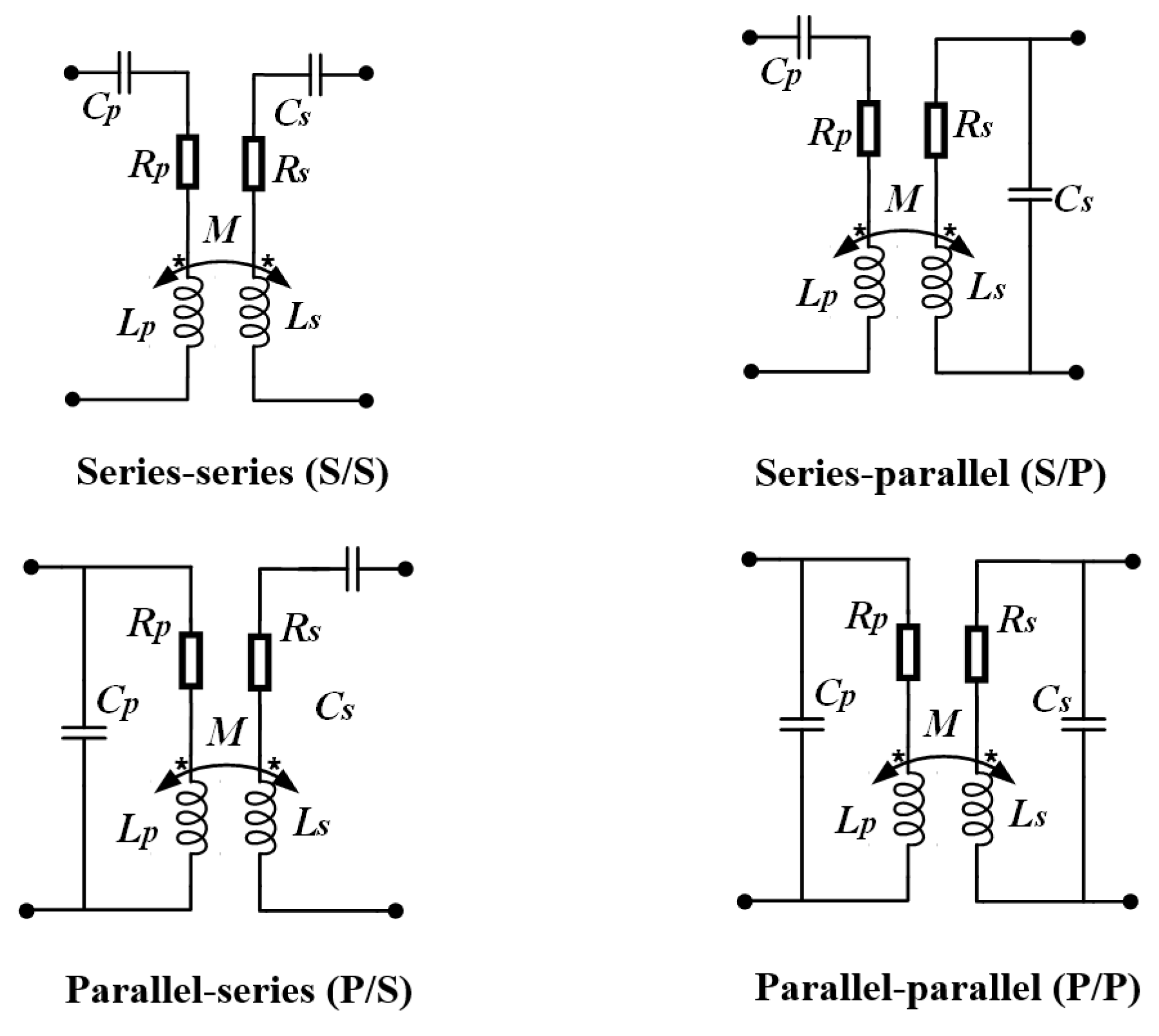
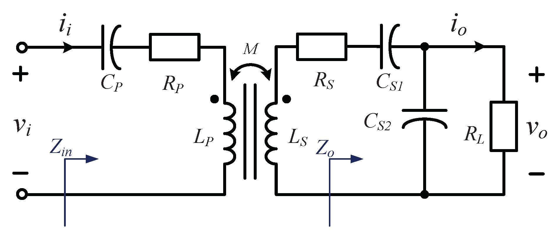
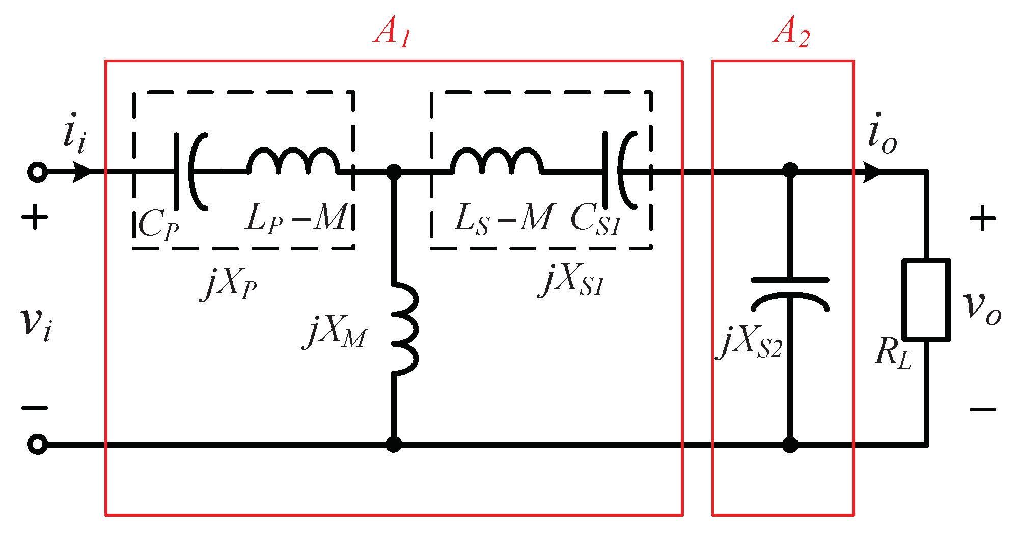
2.1. Fundamental Circuit and Two-Port Network Analysis

In the fundamental circuit model of the S/SP IPT system that is shown in Figure 3, the LCT is formed by two windings of coil, having primary self-inductance L P , secondary self-inductance L S , and mutual inductance M. It is noted that this paper uses subscripts P and S to indicate parameters in the primary and the secondary, respectively. The coupling coefficient is given by
k = M L P L S ,
in practice being affected by the alignment between the primary coil and secondary coil. Both of the coils are series compensated by C P and C S 1 , and an additional capacitor C S 2 is, in parallel connection, in the secondary. Coil losses are represented by resistances R P and R S . R L is the equivalent load resistance. The full bridge inverter generates a high-frequency ac voltage source v i from a dc voltage source. The operating frequency is ω .
Different from a conventional fully compensated series-series IPT system, C P and C S 1 resonate with L P and L S at different angular frequencies, i.e.,
ω P = 1 L P C P ω S = 1 L S C S 1 .
To simplify the analysis, R P and R S can be assumed to be zero for the subsequent analysis of voltage-gain and zero phase angle input [9]. A two-port network can be used to represent the fundamental circuit model, as shown in Figure 4. The two-port network can be expressed by
[ v i , i i ] T = T [ v o , i o ] T .
The transfer matrix A is the product of two sub-transfer matrixes, as
T = T 1 T 2 .
The transfer matrix T 1 is identical to that of a conventional series-series IPT system, while T 2 represents the additional compensation circuit. T 1 and T 2 can be derived as
T 1 = X P + X M X M j X P X S 1 + X M X M + j X S 1 1 j X M X S 1 + X M X M , and T 2 = 1 0 1 j X S 2 1 .
respectively, where X P = ω L P 1 ω C P , X M = 1 ω M , X S 1 = ω L S 1 ω C S 1 and X S 2 = 1 ω C S 2 . Because there only exist linear passive inductors, capacitors, and parasitic resistors in the two-port network T, it is a reciprocal network. Define
T = τ 11 τ 12 τ 21 τ 22 ,
and by the principle of reciprocity, we have
τ 11 τ 22 τ 12 τ 21 = 1 ,
and
v i i i = T v o i o = τ 11 τ 12 τ 21 τ 22 v o i o .
Obviously, from Figure 4, we also have v o = i o R L .
Without a loss of generality, this paper defines λ as the ratio between them
λ = ω P ω S .

2.2. Load-Independent Voltage-Gain with Zero Phase Angle

The voltage-gain of the S/SP IPT system can be defined as
G = v o v i = 1 τ 11 + τ 12 R L .
We can set the R L -related factor in Equation (10) to be zero, i.e., τ 12 = 0 , in order to achieve the load-independent voltage gain and the operating frequency, as given by
G ( ω H ) = L S L P k ( λ 2 + 1 + Δ ) ( 2 k 2 1 ) λ 2 + 1 + Δ
Δ = ( λ 2 1 ) 2 + 4 k 2 λ 2 , and
ω H = ω S 1 + λ 2 + Δ 2 ( 1 k 2 ) λ 1 k 2 ω S , for ( λ 2 1 ) 2 4 k 2 λ 2 .
Figure 5 depicts the voltage-gain G ( ω ) , which varies with the variation of ω under different load conditions. It is noteworthy that G ( ω H ) is independent of the load condition at the operating frequency ω H . A voltage source output is usually desired, because it can simplify the control for output regulation and, thus, such a characteristic is favorable. In fact, the S/SP IPT system can also operate at another operating frequency ω L = ω S λ 2 + 1 Δ 2 ( 1 k 2 ) to achieve another load-independent voltage-gain G ( ω L ) = L S L P k ( λ 2 + 1 Δ ) ( 2 k 2 1 ) λ 2 + 1 + Δ . It should be pointed out that, similar to the case of S/S IPT system, operating at or slightly above ω H , is usually preferred for load-independent voltage-gain, because of easier implementation of ZVS. The simulation parameteres are: L P = 118 μ H, L S = 172 μ H, R P = 0.5 Ω , R S = 0.72 Ω , ω H = 50 kHz, k = 0.15 – 0.3, λ = 1 – 2. They will be used in the rest of the paper, unless specified otherwise.
The input impedance of these IPT systems is given by
Z in = v i i i = a 11 R L + a 12 a 21 R L + a 22 .
To achieve ZPA input, there should has no imaginary component in Z in , i.e.,
( Z in ) = Z in .
Therefore, the design of C S 2 can be derived as
C S 2 = C S 1 ω H 2 ω S 2 1 .

3. Design Considerations

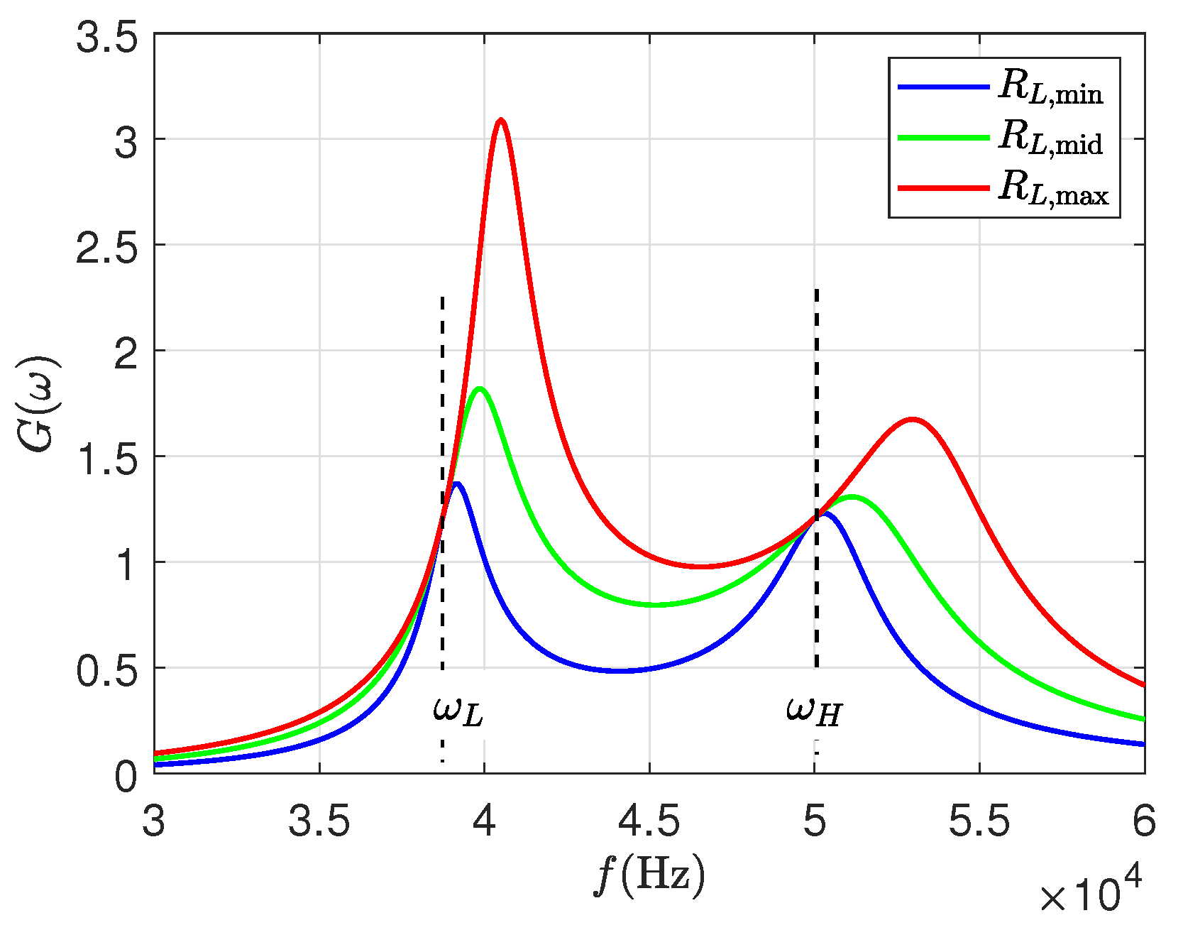
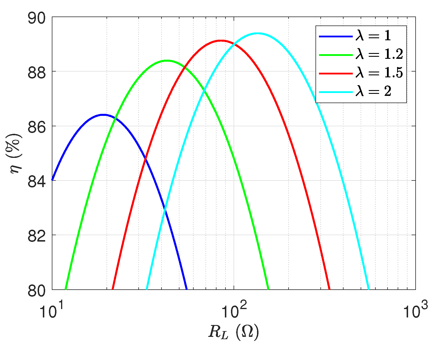
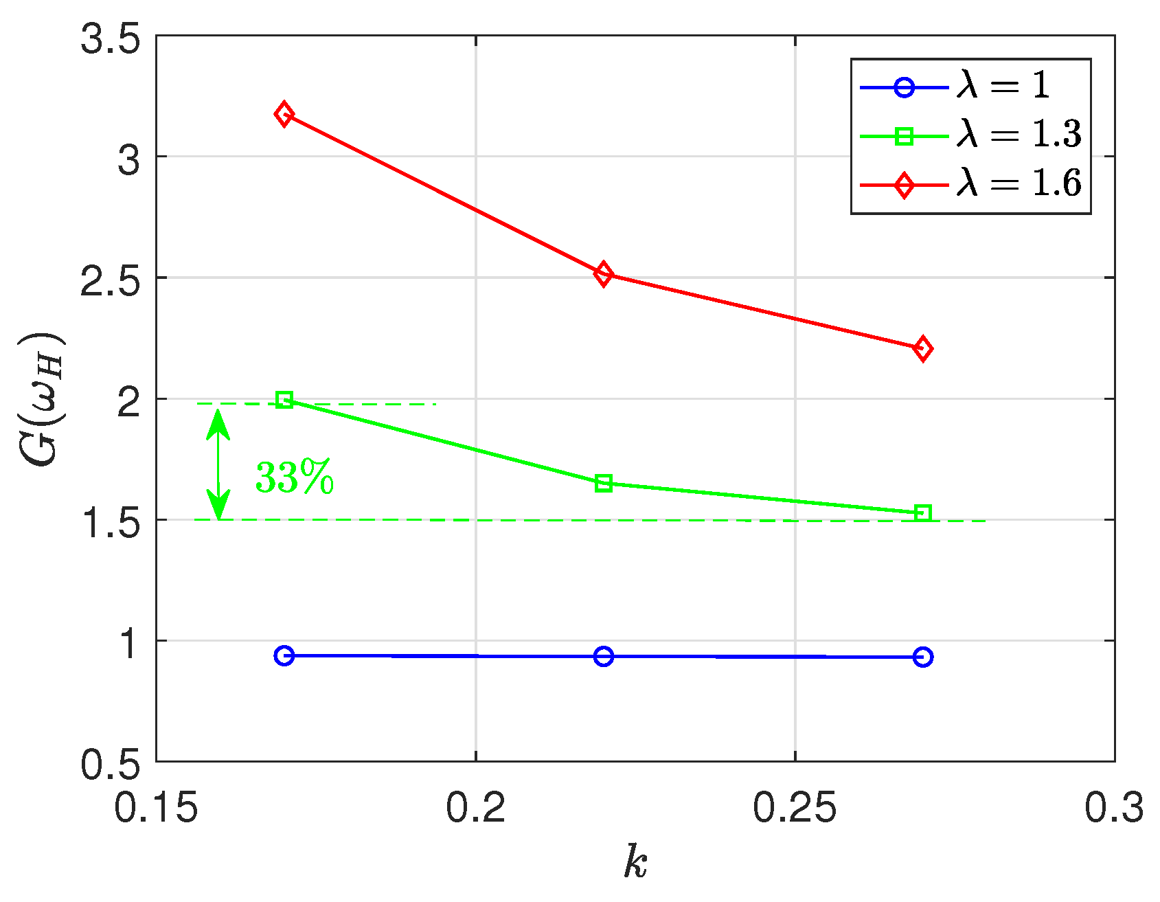
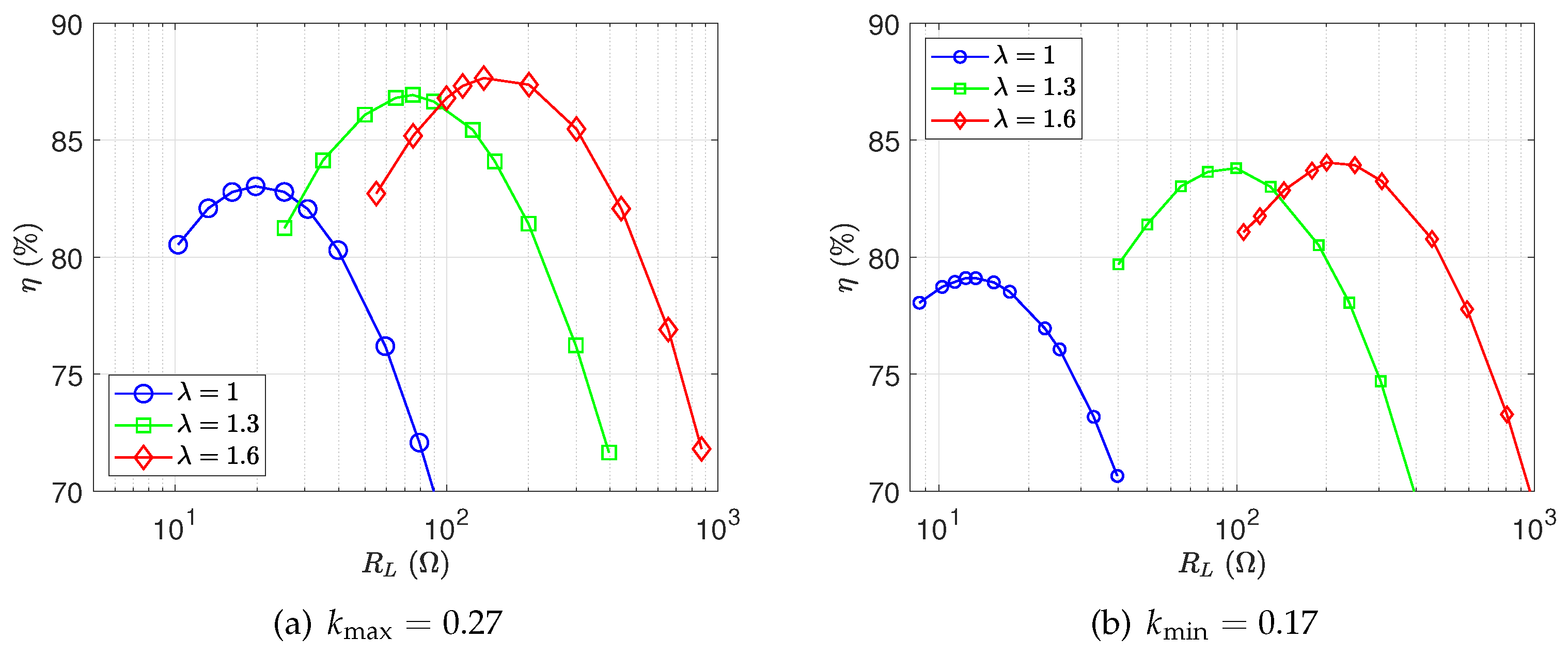
3.1. Efficiency Optimization

The overall power efficiency can be calculated by separately considering the sub-efficiencies in the primary and the secondary, as
η = η P η S , η P = ω 2 M 2 j ω L S + 1 j ω C S 1 + j ω C s 2 R L R P + ω 2 M 2 j ω L S + 1 j ω C S 1 + j ω C s 2 R L , η S = j ω C s 2 R L R S + j ω C s 2 R L ,
where is the real component of the corresponding variable.
In order to conduct a fair comparison of the power efficiency, the operating frequency ω H is first fixed to a constant value, e.g. ω H = ω 0 . Subsequently, different values of λ are designed by choosing compensation capacitors C P , C S 1 , and C S 2 accordingly. By Equations (9), (13) and (16), the design of the compensation parameters is given as
C P = λ 2 + 1 + Δ 2 ( 1 k ) λ 2 ω 0 2 L S ,
C S 1 = λ 2 + 1 + Δ 2 ( 1 k ) ω 0 2 L S ,
C S 2 = λ 2 + 1 + Δ 2 ( 1 k ) ω 0 2 L S λ 2 + 1 + Δ 2 ( 1 k ) 1 .
As an illustration, Figure 6 shows the power efficiency η versus the load resistance R L under different values of λ . It can be observed that the power efficiency can be improved by increasing λ .

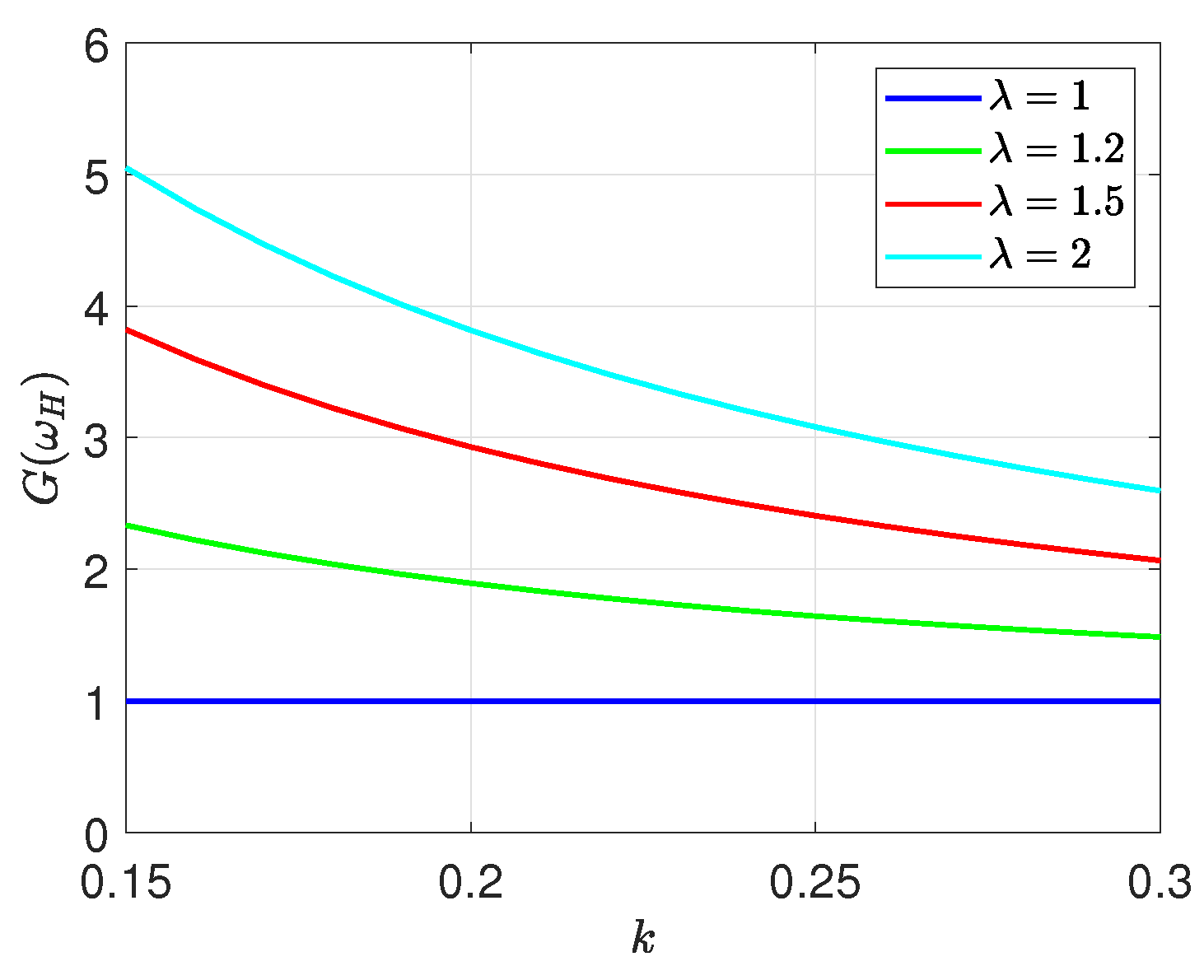
3.2. Constraints Due to Misalignment Issues

Although the voltage-gain of the S/SP IPT system can be load-independent from (11), but there still exists a challenge to the voltage-gain, because G ( ω H ) is k-dependent if λ 1 , which is a common case. Figure 7 shows the load-independent voltage-gain G ( ω H ) versus the coupling coefficient k under different designs of λ . It can be observed that G ( ω H ) is k-independent, only when λ = 1 . As λ increases, G ( ω H ) becomes more sensitive to the coupling coefficient k. Such that there is a constraint to design λ , i.e., λ cannot be infinitely large to maintain an acceptable sensitivity of voltage-gain to misalignment issue. Therefore, a boundary of the acceptable sensitivity of voltage-gain can be defined for the design of λ . For example, α is defined as the acceptable sensitivity of voltage-gain, as given by
G ( ω H ) k min G ( ω H ) k max G ( ω H ) k max α ,
where G ( ω H ) k min is the maximum voltage-gain in the maximum misalignment condition, i.e., k = k min , and G ( ω H ) k max is the rated voltage-gain without misalignment, i.e., k = k max .

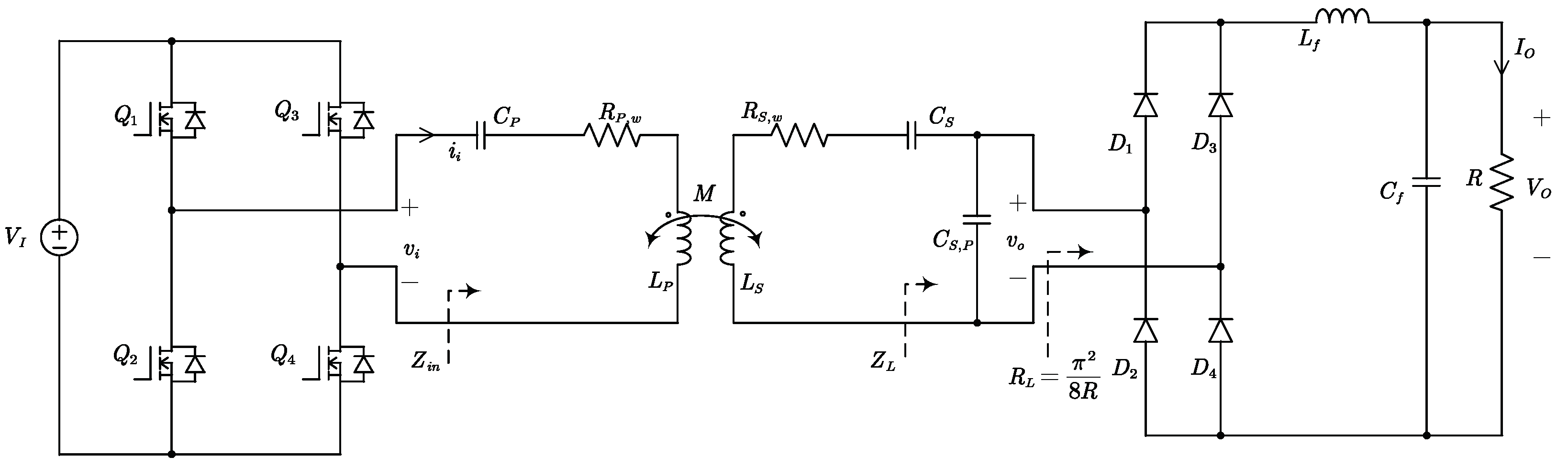
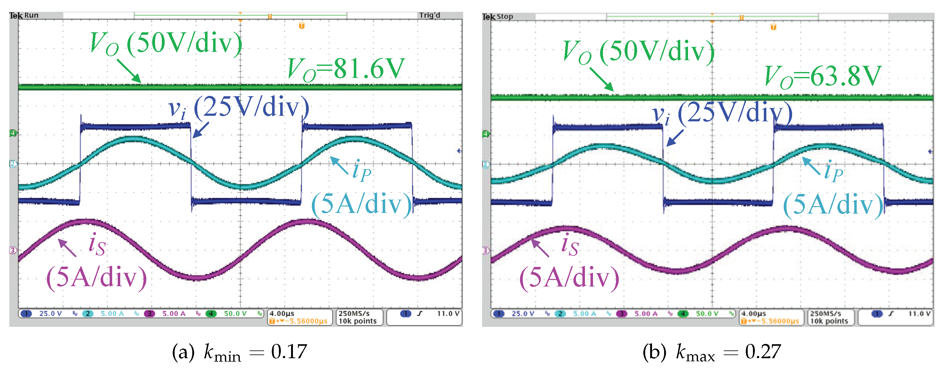
4. Experimental Verification

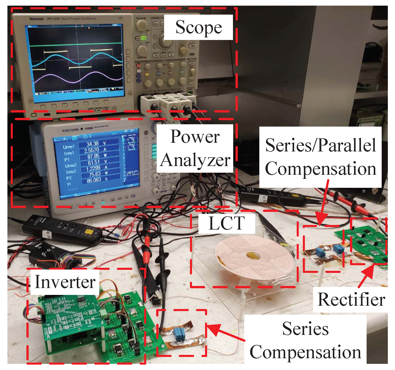
4.1. Experimental Setup

In order to evaluate the S/SP IPT system, an experimental prototype is built with the schematics that are shown in Figure 2. The experimental setup includes an S/SP IPT converter as well as some measurement instruments, as shown in Figure 8. The operating waveforms are captured by an Tektronix DPO 4104 Oscilloscope (Beaverton, OR, USA),the input/output voltages, input/output currents, input/output powers, and efficiencies is measured by a power analyzer YOKOGAWA PX8000 (Tokyo, Japan) and the load is emulated by an electronic load PRODIGIT3302 (Taiwan, China). Table 1 lists the other detailed parameters of the experimental set up, and Table 2 lists the corresponding compensation capacitors under different λ . Meanwhile, for the loosely coupled transform, the magnetic coupled coils in this paper are designed with a circular pad structures and the detailed parameters are listed in Table 3.
In order to verify the performances under different misalignment conditions, there are three misalignment settings in our paper, which correspond to three different coupling coefficients k = 0.17, k = 0.22, and k = 0.27. Meanwhile, the maximum value k = 0.27 is the aligned condition with the air gap 45 mm. In this paper, the misalignment is caused by a position change between the primary and secondary coils in the horizontal direction. The two minimum coupling coefficient k = 0.22 and k = 0.17 correspond to the 25 mm (5% of secondary coil) and 40 mm (12.5% of secondary coil) misalignments from the secondary coil.

4.2. Experimental Results Analysis

The typical steady-state operating waveforms are shown in Figure 9, where ZPA input can be achieved for minimum voltage-ampere rating. Figure 10 depicts the measured load-independent voltage-gain G ( ω H ) , which is consistent with the simulated results that are shown in Figure 7. It should be noted that there exists a scaling factor between the ac voltage gain in Figure 6 and the dc voltage gain in Figure 9, i.e., v o v i = π 2 V O 8 V I . It can be observed that G ( ω H ) can be changed with different values of λ , i.e., different compensation parameters. In addition, for more intuitive display, the numerical measured output voltages V o under different λ and k are listed in Table 4.
In the conventional design [20,21,22], λ is fixed at 1, and the voltage-gain is dependent on the parameters of the LCT, i.e., G ( ω H ) = L S / L P . The drawback is that the change of the voltage-gain requires redesign of the LCT. However, the proposed voltage-gain design depends on the compensation parameters, and there is no need to redesign the LCT. Moreover, the measured load-independent voltage-gain G ( ω H ) versus the coupling coefficient k under different values of λ is also shown in Figure 10. In this study, k varies from 0.17 to 0.27. It is noteworthy that the sensitivity of the voltage-gain increases with λ .
On the other hand, as the measured efficiency η versus R L shown in Figure 11, the efficiency can be improved by λ . The larger λ donates a higher maximum efficiency point. Therefore, there is a trade-off between the sensitivity of the voltage-gain and the efficiency performance, when we design the compensation parameters. In other words, the improvement of the efficiency is limited by the acceptable sensitivity of the voltage-gain. Therefore, the maximum acceptable sensitivity of the voltage-gain α to the variation of coupling coefficient k should be first considered to determine the maximum value of λ . As an example, if we suppose that α 33 % is acceptable, the maximum value of λ can be chosen as 1.3 from Figure 10. Please note that α 33 % means that the variation of voltage-gain is less than 33% when k varies from the nominal value 0.27 to the minimum value 0.17. Therefore, λ = 1.3 can be considered as the boundary of efficiency optimization. It can be observed from Figure 11 that the efficiency can be improved from 83% to 87% and from 79% to 84% when k = 0.27 and k = 0.17 , respectively. Therefore, the efficiency improvement is significant.

5. Conclusions and Discussion

This paper presents a design methodology of the S/SP IPT system to achieve variable load-independent voltage-gains and zero phase angle input over the whole load range. In the conventional design [20,21,22], the voltage-gain is dependent on the parameters of the LCT and, thus, the drawback is that the change of the voltage-gain requires redesign of the LCT. To address this drawback, the proposed design is based on the compensation parameters, and there is no need to redesign the LCT. The effect of the misalignment issue on the voltage-gain is taken into consideration, and design criteria are derived to ensure an acceptable sensitivity to the misalignment when taking efficiency optimization. When the 33% of voltage-gain sensitivity is allowed, a significant efficiency improvement can be achieved from 83% to 87% and from 79% to 84% when k = 0.27 and k = 0.17 , respectively.
The design methodologies of compensation parameters are different when compared with other researches. The change of the voltage gain relies on the redesign of the loosely-coupled transformer, while the compensation parameters should be correspondingly changed as well in present researches. Generally, it is not preferred to redesign the loosely-coupled transformer, because it takes a significant amount of effort. However, the proposed methodology in this paper proposes that the voltage gain can be varied by the design of compensation parameters with the loosely-coupled transformer unchanged. Therefore, we can achieve different voltage gain without the necessity of redesigning the loosely-coupled transformer. Moreover, this paper has in-depth considerations on the efficiency issue and misalignment issue. This paper first found that there is a trade-off between the achievements of high efficiency and low output sensitivity against misalignment issue.

Author Contributions

Conceptualization, L.Y. and M.Z.; methodology, M.Z. and C.L.; validation, L.Y. and C.L.; writing—original draft preparation, L.Y.; writing—review and editing, M.Z. and C.L.; funding acquisition, M.Z. and C.L. All authors have read and agreed to the published version of the manuscript.

Funding

This research was funded by National Key Research and Development Program of China “2018YFB1503004”.

Conflicts of Interest

The authors declare no conflict of interest.

References

  1. Liu, Y.; Li, B.; Huang, M.; Chen, Z.; Zhang, X. An Overview of Regulation Topologies in Resonant Wireless Power Transfer Systems for Consumer Electronics or Bio-Implants. Energies 2018, 11, 1737. [Google Scholar] [CrossRef] [Green Version]
  2. Haerinia, M.; Shadid, R. Wireless Power Transfer Approaches for Medical Implants: A Review. Signals 2020, 1, 209–229. [Google Scholar] [CrossRef]
  3. Liang, C.; Zhang, Y.; Li, Z.; Yuan, F.; Yang, G.; Song, K. Coil Positioning for Wireless Power Transfer System of Automatic Guided Vehicle Based on Magnetic Sensing. Sensors 2020, 20, 5304. [Google Scholar] [CrossRef] [PubMed]
  4. Zhou, J.; Yao, P.; Guo, K.; Cao, P.; Zhang, Y.; Ma, H. A Heterogeneous Inductive Power Transfer System for Electric Vehicles with Spontaneous Constant Current and Constant Voltage Output Features. Electronics 2020, 9, 1978. [Google Scholar] [CrossRef]
  5. Yang, Y.; El Baghdadi, M.; Lan, Y.; Benomar, Y.; Van Mierlo, J.; Hegazy, O. Design Methodology, Modeling, and Comparative Study of Wireless Power Transfer Systems for Electric Vehicles. Energies 2018, 11, 1716. [Google Scholar] [CrossRef] [Green Version]
  6. Wei, X.; Wang, Z.; Dai, H. A Critical Review of Wireless Power Transfer via Strongly Coupled Magnetic Resonances. Energies 2014, 7, 4316–4341. [Google Scholar] [CrossRef] [Green Version]
  7. Xu, H.; Wang, C.; Xia, D.; Liu, Y. Design of Magnetic Coupler for Wireless Power Transfer. Energies 2019, 12, 3000. [Google Scholar] [CrossRef] [Green Version]
  8. Jiang, C.; Chau, K.T.; Liu, C.; Lee, C.H.T. An Overview of Resonant Circuits for Wireless Power Transfer. Energies 2017, 10, 894. [Google Scholar] [CrossRef]
  9. Qu, X.; Jing, Y.; Han, H.; Wong, S.C.; Tse, C.K. Higher Order Compensation for Inductive-Power-Transfer Converters with Constant-Voltage or Constant-Current Output Combating Transformer Parameter Constraints. IEEE Trans. Power Electron. 2017, 32, 394–405. [Google Scholar] [CrossRef]
  10. Truong, C.-T.; Choi, S.-J. Investigation of Scale Conversion for Inductive Power Transfer in Series-Series Configuration. Electronics 2020, 9, 1851. [Google Scholar] [CrossRef]
  11. Shin, H.; Chung, E.; Ha, J.-I. Cost-Effective High-Performance Digital Control Method in Series-Series Compensated Wireless Power Transfer System. Electronics 2020, 9, 1772. [Google Scholar] [CrossRef]
  12. Wang, C.S.; Covic, G.A.; Stielau, O.H. Power Transfer Capability and Bifurcation Phenomena of Loosely Coupled Inductive Power Transfer Systems. IEEE Trans. Ind. Electron. 2004, 51, 148–157. [Google Scholar] [CrossRef]
  13. Zhang, W.; Wong, S.C.; Tse, C.K.; Chen, Q. Analysis and Comparison of Secondary Series- and Parallel-Compensated Inductive Power Transfer Systems Operating for Optimal Efficiency and Load-Independent Voltage-Transfer Ratio. IEEE Trans. Power Electron. 2014, 29, 2979–2990. [Google Scholar] [CrossRef]
  14. Zhang, W.; Wong, S.C.; Tse, C.K.; Chen, Q. Load-Independent Duality of Current and Voltage Outputs of a Series- or Parallel-Compensated Inductive Power Transfer Converter with Optimized Efficiency. IEEE J. Emerg. Sel. Top. Power Electron. 2015, 3, 137–146. [Google Scholar] [CrossRef]
  15. Li, Y.; Hu, J.; Li, X.; Chen, F.; Xu, Q.; Mai, R.; He, Z. Analysis, Design, and Experimental Verification of a Mixed High-Order Compensations-Based WPT System with Constant Current Outputs for Driving Multistring LEDs. IEEE Trans. Ind. Electron. 2020, 67, 203–213. [Google Scholar] [CrossRef]
  16. Qu, X.; Chu, H.; Huang, Z.; Wong, S.C.; Tse, C.K.; Mi, C.C.; Chen, X. Wide Design Range of Constant Output Current Using Double-Sided LC Compensation Circuits for Inductive-Power-Transfer Applications. IEEE Trans. Power Electron. 2019, 34, 2364–2374. [Google Scholar] [CrossRef]
  17. Vu, V.; Tran, D.; Choi, W. Implementation of the Constant Current and Constant Voltage Charge of Inductive Power Transfer Systems with the Double-Sided LCC Compensation Topology for Electric Vehicle Battery Charge Applications. IEEE Trans. Power Electron. 2018, 33, 7398–7410. [Google Scholar] [CrossRef] [Green Version]
  18. Alam, M.M.; Mekhilef, S.; Bassi, H.; Rawa, M.J.H. Analysis of LC-LC2 Compensated Inductive Power Transfer for High Efficiency and Load Independent Voltage Gain. Energies 2018, 11, 2883. [Google Scholar] [CrossRef] [Green Version]
  19. Li, Y.; Hu, J.; Li, X.; Cheng, K.E. A Flexible Load-Independent Multi-Output Wireless Power Transfer System Based on Cascaded Double T-Resonant Circuits: Analysis, Design and Experimental Verification. IEEE Trans. Circuits Syst. I Regul. Pap. 2019, 66, 2803–2812. [Google Scholar] [CrossRef]
  20. Hou, J.; Chen, Q.; Wong, S.C.; Tse, C.K.; Ruan, X. Analysis and Control of Series/Series-Parallel Compensated Resonant Converter for Contactless Power Transfer. IEEE J. Emerg. Sel. Top. Power Electron. 2015, 3, 124–136. [Google Scholar]
  21. Hou, J.; Chen, Q.; Ren, X.; Ruan, X.; Wong, S.C.; Tse, C.K. Precise Characteristics Analysis of Series/Series-Parallel Compensated Contactless Resonant Converterr. IEEE J. Emerg. Sel. Top. Power Electron. 2015, 3, 101–110. [Google Scholar]
  22. Yao, Y.; Wang, Y.; Liu, X.; Lu, K.; Xu, D. Analysis and Design of an S/SP Compensated IPT System to Minimize Output Voltage Fluctuation Versus Coupling Coefficient and Load Variation. IEEE Trans. Veh. Technol. 2018, 67, 9262–9272. [Google Scholar] [CrossRef]
Figure 1. Four basic compensation circuits.
Energies 14 02999 g001
Figure 2. The schematics of the S/SP IPT system.
Energies 14 02999 g002
Figure 3. The fundamental circuit model of the S/SP IPT system.
Energies 14 02999 g003
Figure 4. Two-port network model of the S/SP IPT system.
Energies 14 02999 g004
Figure 5. Load-independent voltage-gain at ω H .
Energies 14 02999 g005
Figure 6. Power efficiency η versus R L under different values of λ .
Energies 14 02999 g006
Figure 7. The load-independent voltage-gain G ( ω H ) versus coupling coefficient k under different values of λ .
Energies 14 02999 g007
Figure 8. Experimental setup.
Energies 14 02999 g008
Figure 9. Steady-state waveforms of v i , i P , i S , and V O of the S/SP IPT system operating at optimum load conditions, under different conditions of coupling coefficient k and with λ = 1.3 . (a) Weak coupled with coupling coefficient k min = 0.17 and (b) Strong coupled with coupling coefficient k min = 0.17 .
Energies 14 02999 g009
Figure 10. The measured load-independent voltage-gain G ( ω H ) versus coupling coefficient k under different values of λ .
Energies 14 02999 g010
Figure 11. Measured efficiency η versus R L , under different conditions of coupling coefficient k and different values of λ . (a) Weak coupled with coupling coefficient k min = 0.17 and (b) Strong coupled with coupling coefficient k min = 0.17 .
Energies 14 02999 g011
Table 1. Parameters of Experimental Prototype.
ParametersSymbolsValues
Input voltage V I 35 V
Switching frequencyf50 kHz
MOSFETs Q 1 Q 4 IPP65R045
Diode D 1 D 4 MBR20200
Dead Time t d e 200 ns
Self inductance L P , L S 117  μ H, 174  μ H
Coupling coefficientk0.17, 0.22, 0.27
Coil resistances R P , R S 0.4  Ω , 0.6  Ω
Table 2. Compensations capacitors of different λ .
Unit (nf) λ = 1 λ = 1.3 λ = 1.6
C P 11074270
C S 1 9895150
C S 2 9414299
Table 3. Parameters of Magnetic coupled coils.
ParametersSymbolsValues
MaterialsLitz WireAWG38
Turns n p , n s 30, 46
Outer Diameter d o _ p , d o _ s 300 mm, 500 mm
Inner Diameter d i n _ p , d i n _ s 35 mm, 35 mm
Radius r p , r s 0.5 mm, 0.75 mm
Table 4. Measured output voltages V o under different k and λ .
Unit (V) λ = 1 λ = 1.3 λ = 1.6
k = 0.17 32.8169.825111.16
k = 0.22 32.757.7588.03
k = 0.27 33.6253.4177.21
Publisher’s Note: MDPI stays neutral with regard to jurisdictional claims in published maps and institutional affiliations.

