Article

Nonlinear Characteristics Compensation of Inverter for Low-Voltage Delta-Connected Induction Motor

1
Energy Internet Engineering Research Center of Chongqing (Chongqing University of Technology), Chongqing 400054, China
2
State Key Laboratory of Power Transmission Equipment & System Security and New Technology, Chongqing University, Chongqing 400044, China
*
Author to whom correspondence should be addressed.
Energies 2020, 13(3), 590; https://doi.org/10.3390/en13030590
Submission received: 30 December 2019 / Revised: 12 January 2020 / Accepted: 24 January 2020 / Published: 28 January 2020
(This article belongs to the Special Issue Electric Vehicle Power Conversion Technologies)

Abstract

:
This paper proposes a scheme that can compensate for the nonlinear characteristics of voltage source inverters (VSIs) for low-voltage delta-connected induction motors (IMs). Due to the nonlinearity introduced by the dead-time, the on/off delay, and the voltage drop across the power device, the output voltage of VSIs is seriously distorted, causing distortion in the phase current of the IM, which will lead to output torque ripple. However, the existing compensation methods for three-phase VSIs are derived from star-connected loads, or ignore the conducting properties of power devices. Moreover, the current polarity detection near the current zero is quite complex. In this paper, by taking such nonlinear characteristics into consideration, especially the conducting property of metal-oxide-semiconductor field effect transistors (MOSFETs), an output voltage model of VSIs for low-voltage delta-connected induction motors is presented. After that, in view of the difficulty in detecting the line current polarity near the current zero which might lead to the wrong compensation, an advancing current crossing zero (ACCZ) compensation is proposed. Subsequently, a compensation scheme which combines the compensation based on the VSI output voltage model and ACCZ compensation is proposed. Finally, the proposed compensation scheme is implemented based on a digital signal processor (DSP) drive system. The experimental results show that the proposed scheme has better performance than the common method in terms of suppressing the effect of the nonlinear characteristics of VSI, which demonstrates that the proposed compensation scheme is feasible and effective for the compensation of the nonlinear characteristics of VSI for low-voltage delta-connected IMs.

Graphical Abstract

1. Introduction

In recent years, the use of low-voltage (48V) induction motor (IM) drive systems has become a trend for both pure electrical vehicles (EVs) and hybrid EVs due to their safety and lack of need of a high-voltage protection device [1]. In such a situation, the high-power battery pack with low-voltage outputs a large current, i.e., several hundred amperes. Thus, a delta-connected IM is better than a star-connected one in low-voltage IM drive systems [2]. However, introducing a delta-connected motor to drive system brings new challenges regarding the compensation of nonlinear characteristics which include dead-time, the on/off delay, and the voltage drop across the power devices in the voltage source inverter (VSI). Such nonlinear characteristics are detrimental to the performance of the inverter, and sequentially lead to large current harmonics as well as torque ripple [3,4].
To mitigate the negative effect of these nonlinear characteristics, two major types of compensation methods have been proposed [5,6,7,8,9,10,11,12,13,14,15]. The first type is to model the nonlinear characteristics as an average voltage loss where the voltage–second is averaged in one pulse-width modulation (PWM) cycle, and then the average voltage loss is added directly to the reference voltage [5,6,7,8,13,14,15]. The second type models the nonlinear characteristics as a pulse shift error which is compensated for in each PWM cycle [9,10,11,12]. A least mean square (LMS)-based algorithm is introduced to decrease the current harmonics caused by dead-time in permanent magnet synchronous motor V/f control systems [13]. The voltage error is estimated by adopting an observer which is based on harmonic analyses and the Kalman filter in the literature [14]. In the literature [15], an adaptive dead-time compensation method is proposed with PWM predictive control. The authors of [16] employed a revised repetitive controller (RRC) to reduce the phase current distortion caused by dead-time. The nonlinear characteristics are compensated for by monitoring the harmonic distortion in the d axis current [17]. A dead-time distortion shaping (DTDS) technique is proposed to displace the energy of the distortion away from the frequency band of interest in [18]. In [19], a graphical solution for compensating voltage error is proposed. Using an adaptive full-order observer, the VSI nonlinear error is compensated for by using feedback gains and self-tuning estimated current errors [20]. However, the existing compensation methods of nonlinear characteristics are based on the star connected load. Therefore, compensation based on the output voltage model of the VSI for delta-connected IMs should be rederived. Meanwhile, in [8,9], the voltage drop across the power device is ignored, and only dead-time and the on/off delay are compensated for. The authors of [4,7,10] built the output voltage model of VSI with a constant voltage drop across the power device. In low-voltage inverters, the metal oxide semiconductor field effect transistor (MOSFET) is the first choice for the power device in low-voltage inverters because it has more efficient performance than insulated gate bipolar translators (IGBTs) [21,22]. Due to the conductance modulation effect, the voltage drop observed in IGBTs could be regarded as a constant, which makes it possible that the compensation could be calculated offline [22]. However, there is no conductance modulation effect for MOSFETs. Therefore, MOSFETs have the property of resistance when they conduct. In fact, the voltage drop across MOSFETs should be regarded as a current-related variable, which has to be calculated online, rather than a constant [21]. More importantly, compared to high-voltage systems, the voltage drop across power devices in low-voltage induction motor drive systems is considerably higher because of the large current.
In addition, the line current polarity near the zero is difficult to detect due to the inevitable current ripple. In [23], accurate current polarity detection is implemented by a current polarity detection circuit and a field-programmable gate array (FPGA) in the VSI. Although this guarantees the accuracy of the detection, the cost increases at the same time. A method which filters the current and takes the results as the current polarity is proposed in [6]; however, it causes a phase delay and requires complex calculations. To simplify detection, the reference current polarity is regarded as the most practical current polarity method in the realization of compensation [8]. There is no doubt that this works in steady-state systems. Nevertheless, for EV drive systems, the error cannot be ignored. Thus, to compensate for the nonlinear characteristics of the VSI for low-voltage, delta-connected IMs, the conducting properties of the power device should be taken into consideration. Furthermore, the compensation value should be derived under delta-connected load conditions. Moreover, a current detection method near the zero point should be simplified.
This paper mainly focuses on the compensation for the nonlinear characteristics for low-voltage induction motor drive systems. In Section 2, the output voltage model of a VSI for a low-voltage, delta-connected IM is given, and the voltage drop across the MOSFET is modeled according to its conducting properties. In Section 3, a compensation scheme based on the output voltage model of the VSI for the delta-connected IM is proposed. Then, to overcome the difficulty of current polarity detection near zero, advancing current crossing zero (ACCZ) compensation is proposed. Finally, a compensation scheme which combines the two aforementioned compensation modes is proposed. In Section 4, by comparing the results of the experiment with no compensation and another common compensation method, the validity of the proposed compensation scheme is verified.

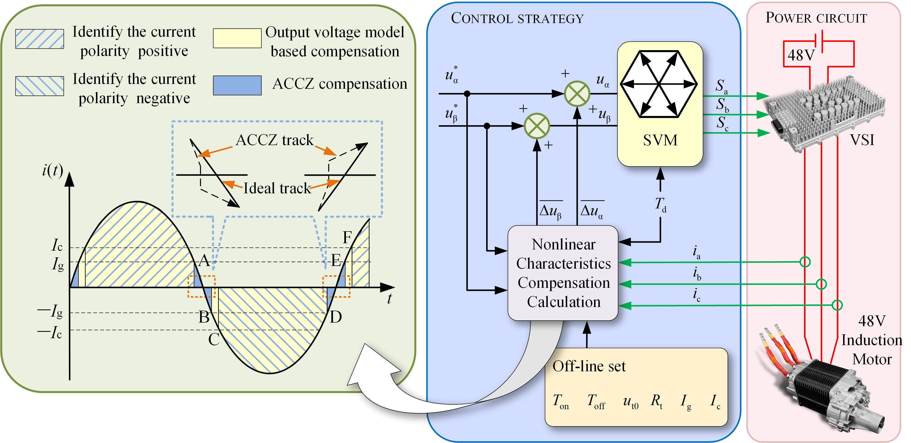
2. Nonlinear Characteristics of the Inverter for Low-Voltage Electric Vehicles

There are two major types of inverter nonlinear characteristics, namely, the PWM cycle time error and the voltage drop across the power device. The PWM cycle time error contains the dead-time and the on/off delay for power device. On most occasions, the voltage drop across the power device can be deemed as a constant; however, in the VSI for low-voltage IMs, it should be treated as a variable which is associated with the conducting current [21]. All these factors must be tackled to obtain satisfactory performance from a VSI for a low-voltage IM.

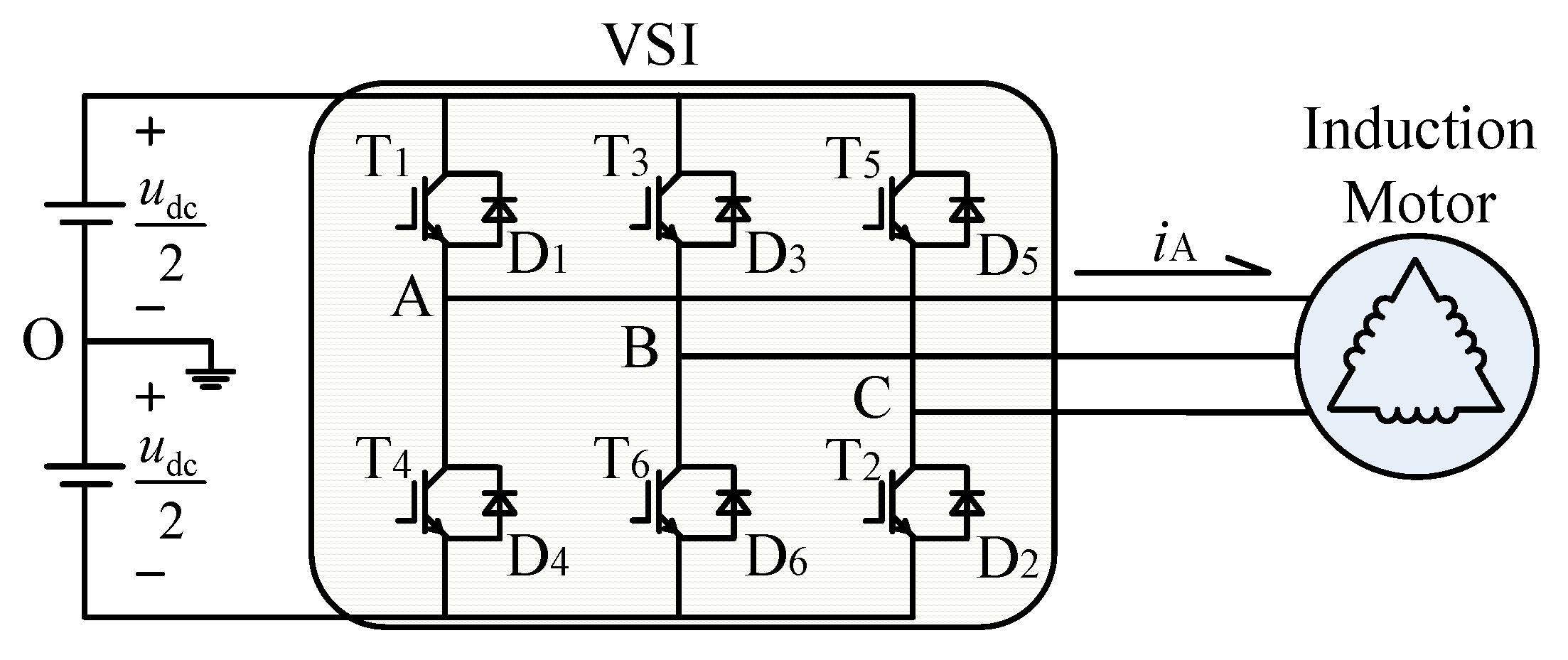
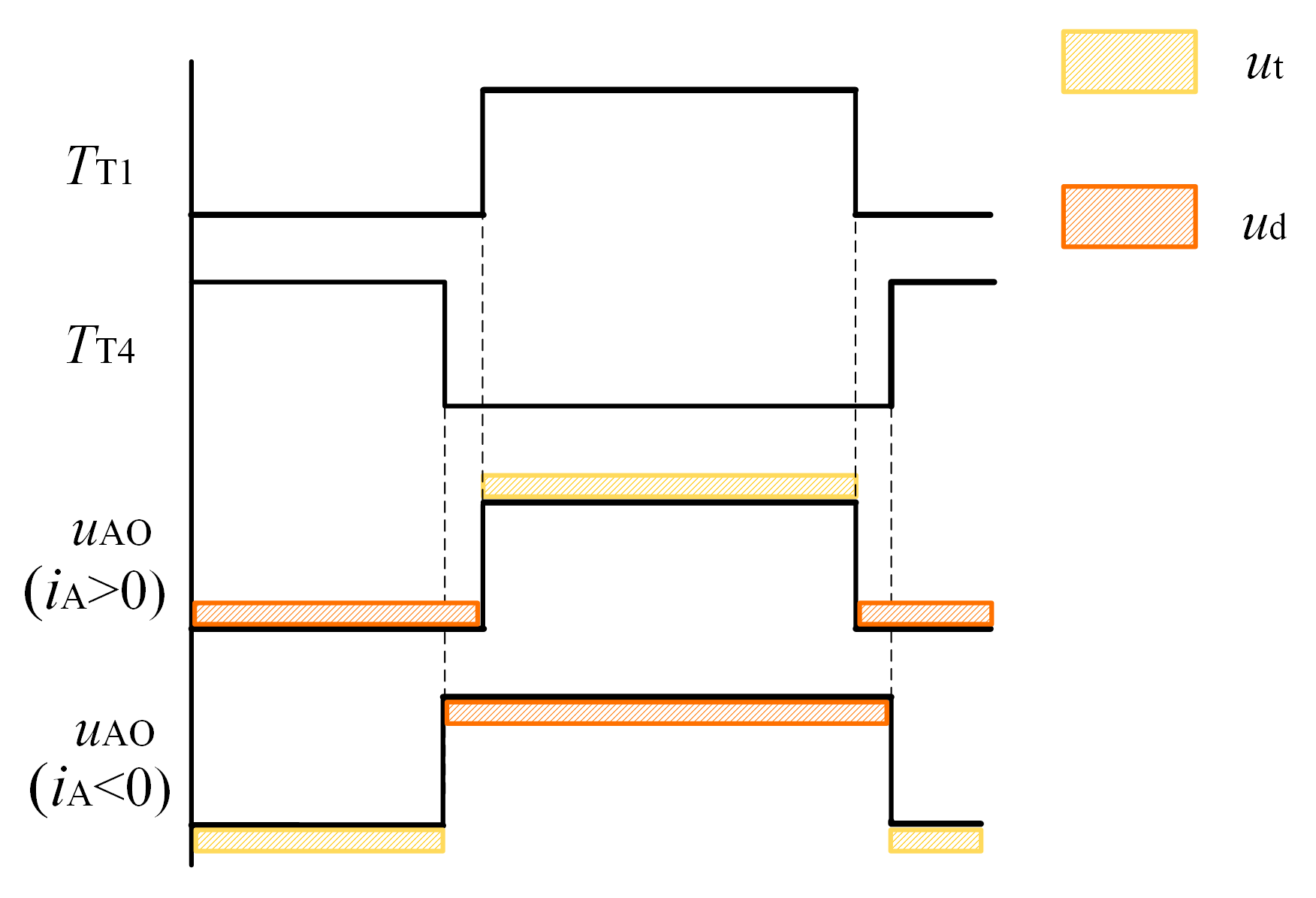
2.1. Dead-time and Turn-on/off Delay

The typical MOSFET-based three-phase VSI topology with a delta-connected IM load is shown in Figure 1. T1–T6 represent the MOSFETs and D1–D6 represent the antiparallel diodes. Point O is the power neutral and iA is the current in phase A of VSI or the line current of the IM. The time required for the MOSFET to turn on and off are denoted by Ton and Toff, respectively. It is essential to set a dead-time (Td) between MOSFET T1 and T4 (T3 and T6, T5 and T2) in order to prevent short circuits in any of the legs of the VSI. The parasitic parameters of power devices and possible buffer circuits are ignored in this paper.
The three phases in a motor drive system can be assumed to generally be identical, so only phase A in the VSI is analyzed below. The current direction is defined as positive, as shown in Figure 1. In addition, the gate drive signals for MOSFETs and the corresponding output voltage waveforms of the VSI legs (uAO) under different current polarities are shown in Figure 2 [10]. In one PWM cycle, the ideal conducting time for phase A in the VSI is TAideal, and the average reference voltage is
u AOset ¯ = u dc T Aideal T s
where udc is the dc bus voltage and Ts is the switching period.
With a dead-time on the pulse rising edge, the practical gate drive signals for T1 and T4 are ST1 and ST4 respectively. Due to the MOSFET’s turn on and off time delay, the practical conducting time for T1 and T4 are TT1 and TT4, respectively. As a result, the output voltage of the VSI legs can be derived under different current polarities. From Figure 2, the average voltage error in one PWM cycle can be expressed as (2), which varies with the current polarity indicated by sign function
Δ u AO ¯ = u err sign ( i A )
where sign (iA) is the sign function, which can be defined as
sign ( i A ) = { 1 1 i A > 0 i A < 0
where iA is the current in phase A of VSI, or the line current of the IM. uerr is defined as
u err = u dc ( T d + T on T off ) T s
So, the practical conducting time in one PWM cycle for phase A can be derived as
T A = T Aideal + sign ( i A ) ( T d + T on T off )

2.2. Voltage Drop Across the MOSFET

For general motor drive systems, the impact of voltage drop across power devices is negligible. However, such an impact cannot be ignored if we wish to obtain a precise supply voltage and a stable torque output. Specially in low-voltage motor drive systems, large currents will make the voltage drop even larger. Hence, we cannot consider the voltage drop to be constant. However, it should be a variable which is related to the conducting current.
The impact of the voltage drop across power devices in one PWM cycle is shown in Figure 3. TT1 and TT4 are the practical conducting time for MOSFET T1 and T4. Due to the voltage drop across the power device, the practical output voltage of the VSI legs is uAO under different current polarities [12]. As a consequence, the output voltage of the VSI legs can be expressed as (6), according to Figure 3
u AO = ( u dc u t + u d ) ( K A 1 2 ) 1 2 sign ( i A ) ( u t + u d )
where ut is the voltage drop across the MOSFET, and ud is the voltage drop across the antiparallel diode. KA = 1 when the phase A drive pulse is at a high level, and KA = 0 when the phase A drive pulse is at a low level.
Thus, the average output voltage in one PWM cycle can be derived as
u AO ¯ = ( u dc u t + u d ) ( T A T s 1 2 ) 1 2 sign ( i A ) ( u t + u d )
According to the above analysis, the voltage drop across the MOSFET is related to the conducting current. Moreover, the MOSFET presents resistance properties when it is conducting; thus, according to [17], the relationship between the voltage drop across the MOSFET and the conducting current can be derived as (8):
u t = u t 0 + R t | i A |
where ut0 is the cut-off voltage and Rt is the conducting resistance of MOSFET.
As a result, in the VSI for low-voltage motor drive systems, the average output voltage for phase A with consideration of the voltage drop across the MOSFET can be expressed according to (5), (7), and (8)
u AO ¯ = ( u dc u t 0 + R t | i A | + u d ) [ T Aideal + sign ( i A ) ( T d + T on T off ) T s 1 2 ] 1 2 sign ( i A ) ( u t 0 + R t | i A | + u d )
Similarly, we can get u BO ¯ and u CO ¯ ; then, the output voltage model of the VSI for low-voltage motor drive systems is complete.

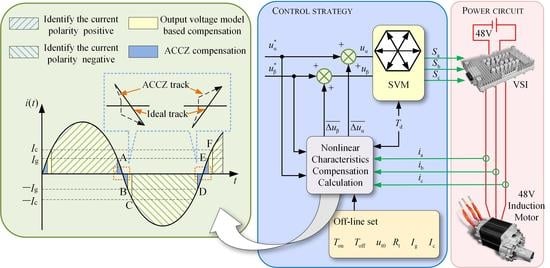
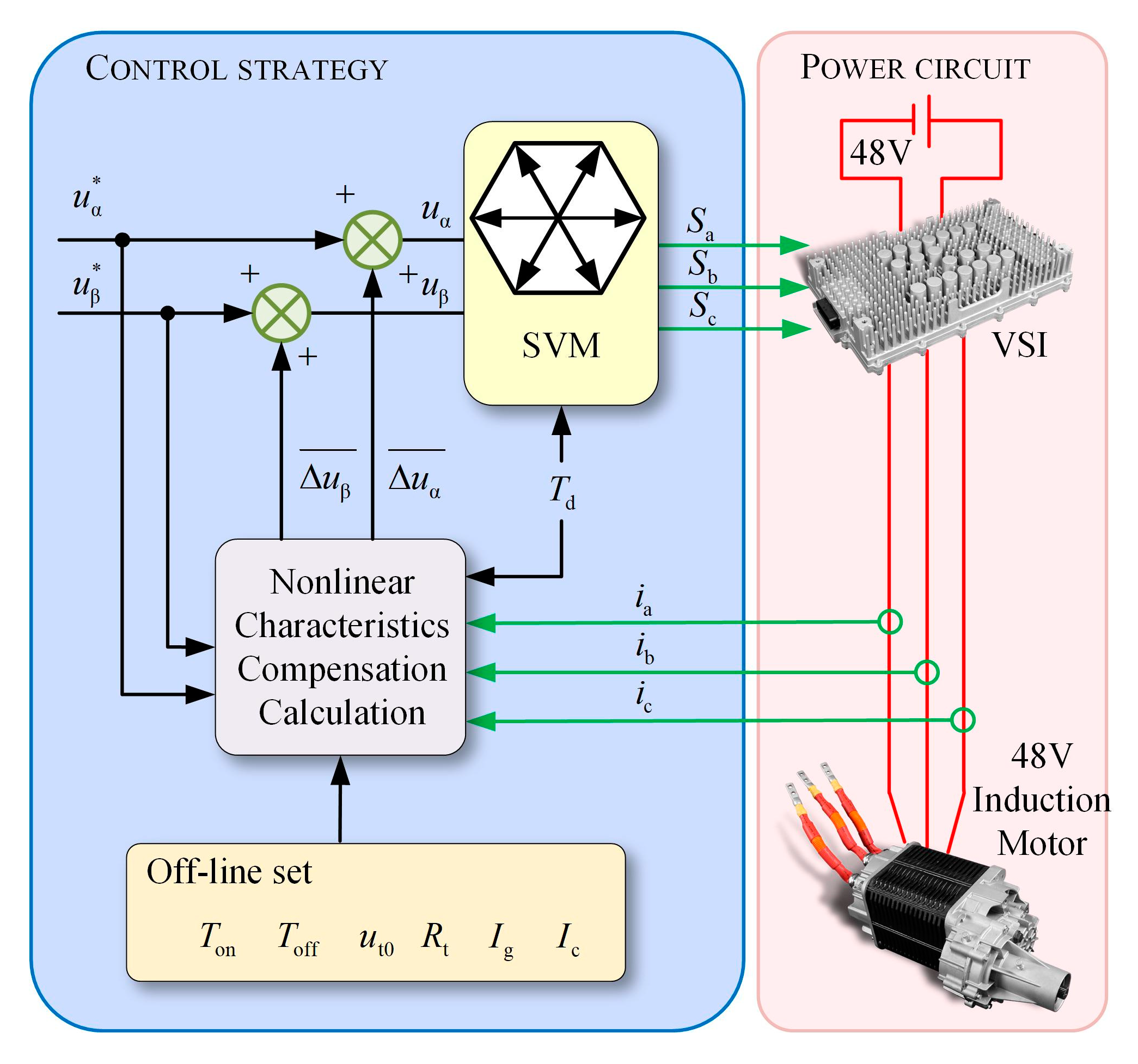
3. The Proposed Compensation Scheme

There are two modes in the proposed compensation scheme, namely, compensation based on the output voltage model of the VSI and ACCZ compensation. The mode of compensation depends on the state of the current.

3.1. Compensation based on the Output Voltage Model of VSI

According to (1), (5), and (9), the average voltage error in one PWM cycle can be obtained from the output voltage model of the VSI and the reference voltage in phase A
Δ u AO ¯ = u AOset ¯ u AO ¯ = u dc T Aideal T s ( u dc u t 0 + R t | i A | + u d ) ( T Aideal + sign ( i A ) ( T d + T on T off ) T s 1 2 ) 1 2 sign ( i A ) ( u t 0 + R t | i A | + u d )
Similarly, we can get Δ u BO ¯ and Δ u CO ¯ . As shown in Figure 1, 48V IM is delta connected. The relationship between the phase voltage of the stator and the output voltage of the VSI legs can be expressed as
{ u Ap = u AO u BO u Bp = u BO u CO u Cp = u CO u AO
where uAp, uBp, and uCp are the stator phase voltage.
For Clark transformation [13],
[ u α u β ] = 2 3 [ 1 1 2 1 2 0 3 2 3 2 ] [ u Ap u Bp u Cp ]
where uα and uβ are the stator phase voltage in α–β reference frame.
Hence, in α–β reference frame, (12) can be rewritten as follows according to (11):
[ u α u β ] = [ 1 1 0 1 3 1 3 2 3 ] [ u AO u BO u CO ]
Similarly, the relationship between the average error voltage in the two-phase stationary coordinate system and the average output voltage of the VSI legs in one PWM cycle can be expressed as:
[ Δ u α ¯ Δ u β ¯ ] = [ 1 1 0 1 3 1 3 2 3 ] [ Δ u AO ¯ Δ u BO ¯ Δ u CO ¯ ]
where Δ u α ¯ and Δ u β ¯ are the stator phase voltage error in α–β reference frame, and Δ u AO ¯ , Δ u BO ¯ , and Δ u CO ¯ are the output voltage error of the VSI legs. Based on (10) and (14), the reference voltage of space vector modulation (SVM) is compensated for:
{ u α = u α * + Δ u α ¯ u β = u β * + Δ u β ¯
where uα and uβ are the set value of the reference voltage of SVM, and uα* and uβ* are the actual value of the reference voltage of SVM. From (15), the error voltage in the two-phase stationary coordinate system is directly added to the reference voltage of the SVM, and the output voltage of the VSI can be compensated for accurately. Meanwhile, it is noteworthy that the SVM modulation strategy for a delta-connected load should be rederived.

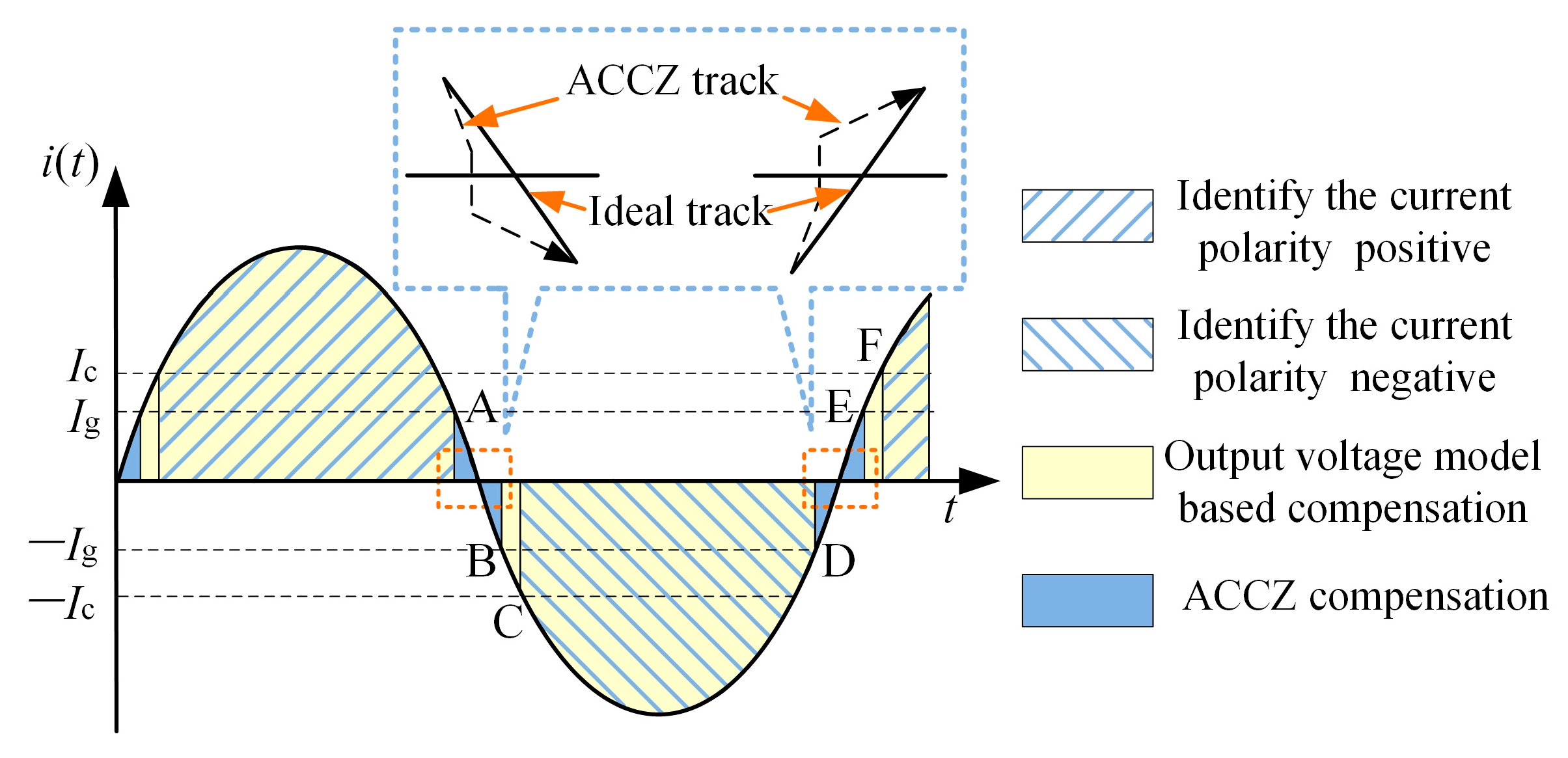
3.2. Advancing Current Crossing Zero (ACCZ) Compensation

According to the above analysis, the error voltage caused by nonlinear characteristics is related to the magnitude and polarity of the current in each phase of the VSI. When the current crosses zero, the polarity of the current may be judged incorrectly due to the zero current clamping effect and the current burr during detection. As a result, a wrong compensation will be caused. To get the accurate polarity of the current, the methods mentioned in Section 1, which include filtering the current or adopting the reference current as the practical current polarity, cannot be applied for EV drive systems. A method requiring fewer calculations should be proposed for low-voltage EVs.
It can be seen from (10) that when the current is nonzero, the current and the compensation voltage always show opposite polarities to each other. Therefore, at this point, applying a compensation voltage which has the same polarity to the current will accelerate the current crossing zero, as shown in Figure 4. Therefore, when the current polarity is difficult to detect and the current has not crossed zero, if we still adopt the compensation value based on the output voltage model of the VSI (such a compensation value is hereafter referred to as ε ), incorrect compensation may result. Instead, we can assume the current has already crossed zero, and then set the compensation value magnitude to ε with the polarity opposite to ε, and maintain this compensation value. Such a compensation value will accelerate the process of the current crossing zero. After the current crosses zero and reaches a certain value, we can return to the compensation based on the output voltage model of the VSI. Because the zero crossing is accelerated, the zero current clamping effect will only occur for a very short time, which has little influence on the whole waveform. In other words, the overall development direction of the current is completely correct. Therefore, the problem of determining the direction of the current can be solved by simply advancing the current crossing zero compensation.
The specific determination method of current direction is shown in Figure 4. Firstly, we can set two current limits, Ig and Ic, according to the actual working condition of the IM and the current detection noise tolerance. In the segment AC of Figure 4, before the current is less than Ig (point A in Figure 4), the current polarity can be determined to be positive. Once the current is lower than Ig, it is assumed that the current will continue to develop in a negative direction, and therefore, that the polarity cannot be detected accurately. The compensation value is set as the opposite number of the compensation value (ε) when the current is equal to Ig until the current is less than −Ig (point B in Figure 4). At the same time, in order to avoid burr interference in the current detection near point B, the negative polarity of the current is not determined until the current is less than −Ic (point C in Figure 4). After the current is less than −Ic, we can compensate according to the output voltage model of the VSI.
Conversely, in segment DF of Figure 4, before the current is more than −Ig (point D in Figure 4), we can determine that the current polarity is negative. Once the current is more than −Ig, we can assume that current will continue to develop in a positive direction, and that the polarity cannot be accurately detected again. The compensation value is set as the opposite number of the compensation value when the current is equal to −Ig, until the current is more than Ig (point E in Figure 4). Similarly, in order to avoid burr interference in the current detection near point E, the negative polarity of the current is not determined until the current is more than Ic (point F in Figure 4). After the current is less more than Ic, we can compensate according to the output voltage model of the VSI, and enter the next current cycle.

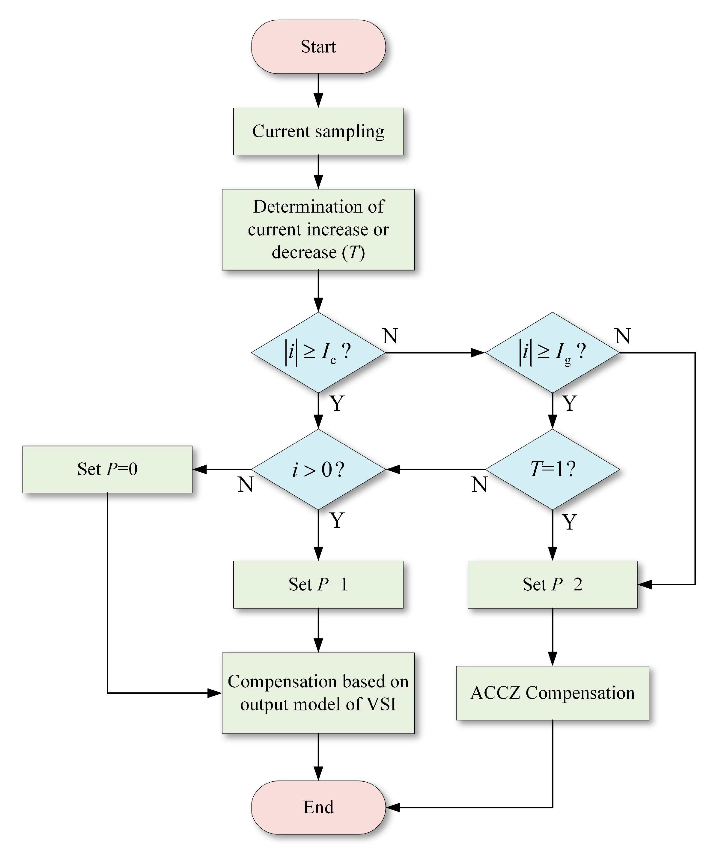
3.3. A combination of Two Compensation Modes

To realize the two compensation modes described above, a determination strategy was carried out, as shown in Figure 5.
In Figure 5, we begin with the current sampling, and get the current value i. Next, by comparing with the current samples several PWM cycles ago, we can determine whether the current is increasing or decreasing. We built function T to indicate whether the current was increasing or decreasing. When T = 1, the current was increasing. When T = 0, the current was decreasing. Then, the compensation mode is determined by the judgment condition described in Section 3.2, and the current value i. During the determination and calculation, we created the current polarity function P for convenience. When P = 0, the current polarity is negative. When P = 1, the current polarity is positive. When P = 2, the current polarity is assumed to be undetectable. The control strategy diagram for the proposed compensation scheme is shown in Figure 6.

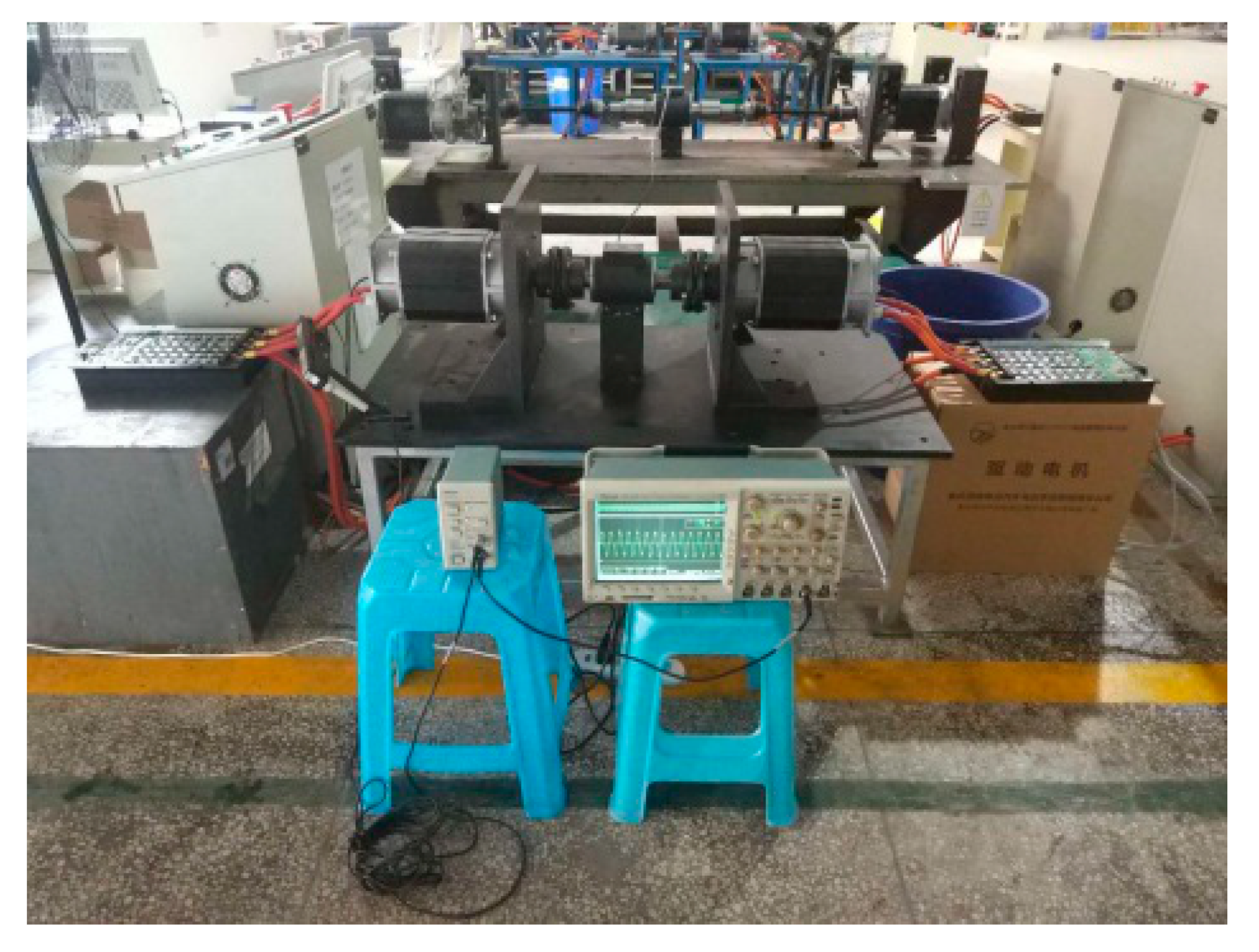
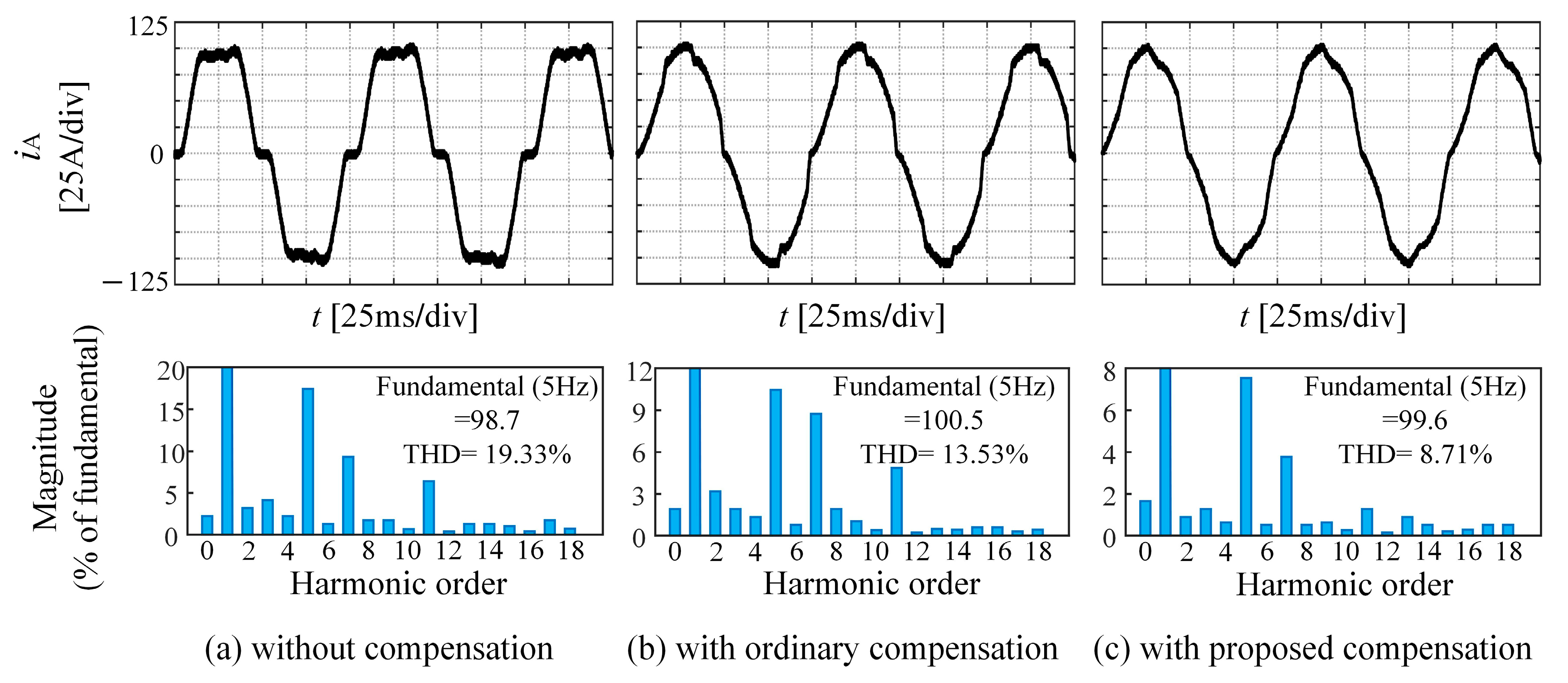
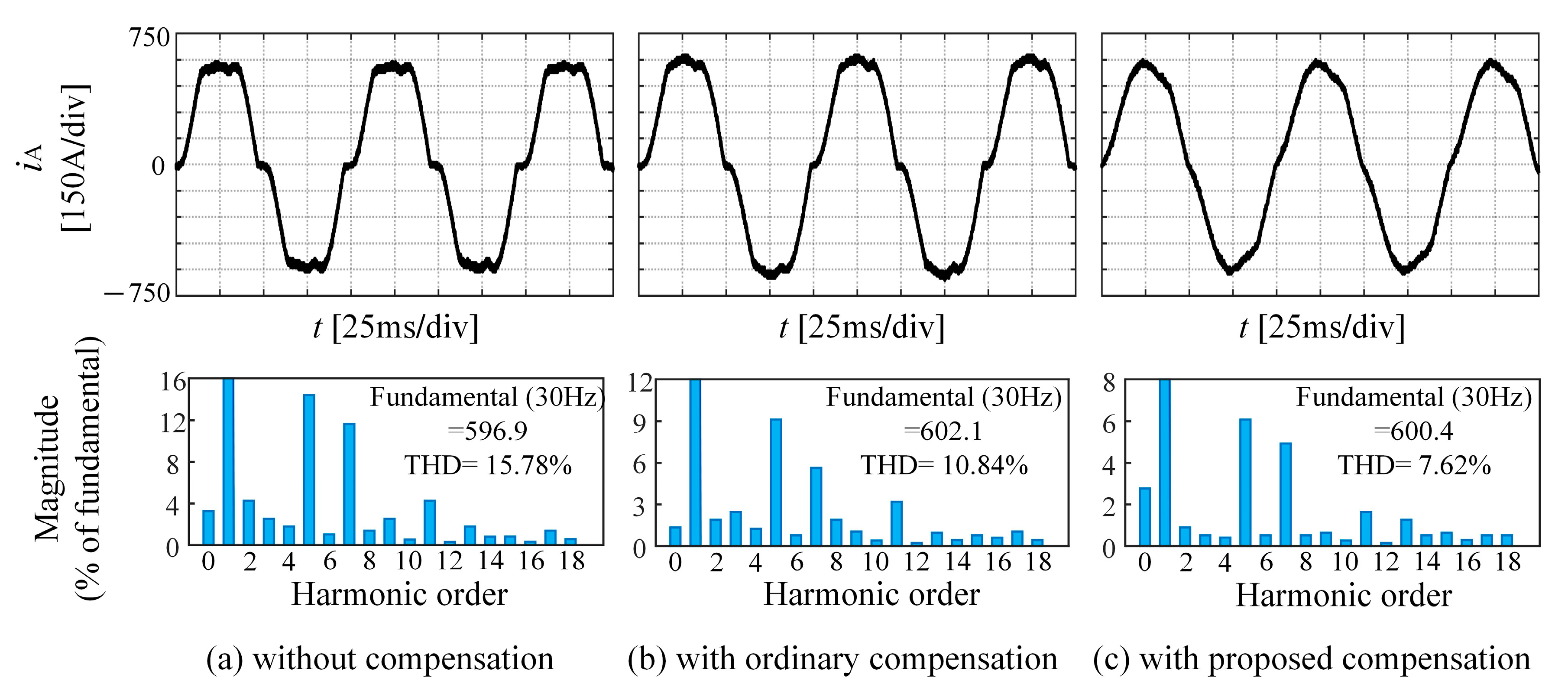
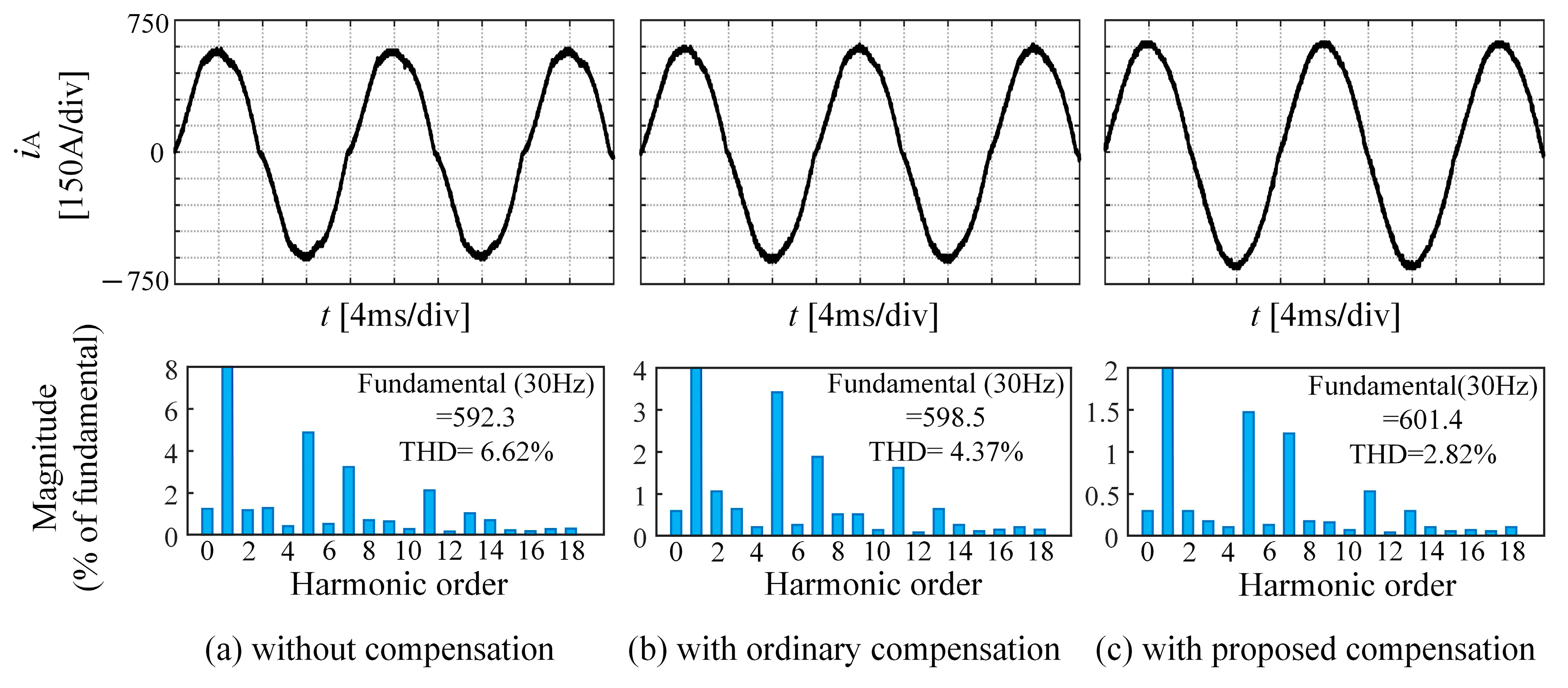
4. Experimental Verification

In order to verify the proposed compensation scheme, experiments were implemented on a digital signal processor (DSP) drive system. The experiments were done with 2 μs dead-time and a 15 kHz switching frequency. The parameters of the 48V IM are shown in Table 1. For the MOSFET (STH15810-2), the conducting resistance is 0.0039 Ω with ut0 = 0.43V, and the on/off delays are 33 ns and 72 ns, respectively, while Ig and Ic are set as 4 A and 8 A, respectively. DSP tms320-f28035 is adopted as the controller of the system to build the VSI induction motor driving experimental platform. Due to the 15 kHz switching frequency, the current sampling delay and the effect of discretization to realize digital control are neglected.
The experimental platform of the 48 V IM drive system is shown in Figure 7. To get better observations of the experiment and the data results, the drive system adopted a variable-voltage variable-frequency (VVVF) control strategy rather than field orient control (FOC). Three different voltage/frequencies were set without load: 5 V/5 Hz, 30 V/5 Hz, and 30 V/30 Hz. Furthermore, three different kinds of compensations were adopted: no compensation, a common compensation scheme (taking Td, Ton, and Toff into consideration, treating ut as a constant, with no more other compensation near current zero), and the proposed compensation scheme. We observed a phase A current waveform, as shown in Figure 8, Figure 9 and Figure 10, using the POWERGUI/FFT tool module in SIMULINK, and analyzed the current waveform, thereby obtaining the corresponding current total harmonic distortion (THD), as shown in Table 2.
From the corresponding current waveform and THD analyses shown in Figure 8, we can see that both the common compensation method and the proposed compensation scheme can compensate for the nonlinear characteristics well under 5 V/5 Hz, and that the corresponding current THD for iA are 19.33%, 15.33%, and 13.74% respectively. Due to the low current for this condition, the common compensation method treating ut as a constant would not cause significant errors in compensation.
At a given voltage of 30 V/5 Hz conditions, the current increases, and the voltage drop across power devices changes. Therefore, the proposed synthetic compensation scheme has a better compensation effect than the common compensation method. As shown in Figure 9 and Table 2, the proposed compensation scheme can limit the current THD to 7.62%, while the current THD under the common compensation method reached 10.84%.
Under the condition that of voltage = 30 V/30 Hz, the current also increases, and the forward voltage drop for devices changes. Therefore, it can no longer be regarded as a constant value in compensation calculations; to do so would cause the problem of inaccurate compensation. As shown in Figure 10 and Table 2, the common compensation method cannot effectively compensate for the nonlinear characteristics of the inverter because the current THD only decreases by 2.25%, compared with the uncompensated current THD (6.62%). By contrast, the proposed compensation scheme can significantly improve the current waveform quality. The current THD is 2.82%, which decreases by 3.80% compared with the uncompensated current THD, and 1.55% compared with the common compensation method. This means the proposed compensation scheme can achieve the ideal compensation effect.
At the same time, it can be seen from Figure 8c, Figure 9c, and Figure 10c that the currents have the tendency to cross through the zero in advance near the zero due to the ACCZ compensation, which effectively inhibits the effect of zero current clamping, and avoids the complex detection required for current polarities near zero.

5. Conclusions

This paper analyzes the influence of nonlinear characteristics on the VSI for low-voltage EVs. Firstly, the output voltage model, which takes the conducting property of the MOSFET into consideration, was created. Next, an ACCZ compensation was also introduced for compensation when the current is near zero. Moreover, a compensation scheme based on a combination of the output voltage model and ACCZ is proposed. Finally, the proposed compensation scheme is verified on a 48V IM drive system experiment platform. From the experiment results, we observed that the phase current waveforms under the proposed compensation scheme had lower THD than those under the common compensation method with different voltage sets. The currents also had the tendency to cross through the zero in advance near the zero. The main conclusions of this paper may be summarized as follows:
  • Compensation according to the VSI output voltage model with consideration of the conducting properties of MOSFET has a better effect than the common compensation method.
  • ACCZ compensation not only avoids the complicated calculations required for current polarity, but also effectively inhibits the current waveform distortion near current zero.
  • The proposed compensation scheme based on the combination of the output voltage model and ACCZ is suitable for nonlinear characteristics compensation for VSIs for low-voltage, delta-connected IMs.

Author Contributions

Conceptualization, Z.D., and Q.G.; Methodology, Z.D.; Software, X.Y.; Validation, Z.D. and X.Y.; Formal analysis, Z.D.; Writing—Original Draft Preparation, Z.D.; Writing—Review & Editing, Q.G., and H.L.; Funding acquisition, Q.G. and H.L. All authors have read and agreed to the published version of the manuscript.

Funding

This research was supported by the Science and Technology Research Program of Chongqing Municipal Education Commission (KJ1600944).

Conflicts of Interest

The authors declare no conflict of interest.

References

  1. Wearing, A.D.; Haybittle, J.; Bao, R.; Baxter, J.W.; Rouaud, C.; Taskin, O. Development Of High Power 48V Powertrain Components For Mild Hybrid Light Duty Vehicle Applications. In Proceedings of the 2018 IEEE Energy Conversion Congress and Exposition, Portland, OR, USA, 23–27 September 2018; pp. 3893–3900. [Google Scholar]
  2. Ferreira, F.J.T.E.; Silva, A.M.; Cruz, S.M.A.; De Almeida, A.T. Comparison of Losses in Star- and Delta-Connected Induction Motors with Saturated Core. In Proceedings of the 2017 IEEE International Electric Machines and Drives Conference, Miami, FL, USA, 21–24 May 2017. [Google Scholar]
  3. Lee, K.; Yao, W.; Chen, B.; Lu, Z.; Yu, A.; Li, D. Stability Analysis and Mitigation of Oscillation in an Induction Machine. IEEE Trans. Ind. Appl. 2014, 50, 3767–3776. [Google Scholar] [CrossRef]
  4. Guha, A.; Narayanan, G. Impact of Undercompensation and Overcompensation of Dead-Time Effect on Small-Signal Stability of Induction Motor Drive. IEEE Trans. Ind. Appl. 2018, 54, 6027–6041. [Google Scholar] [CrossRef]
  5. Li, P.; Zhang, L.; Ouyang, B.; Liu, Y. Nonlinear Effects of Three-Level Neutral-Point Clamped Inverter on Speed Sensorless Control of Induction Motor. Electronics 2019, 8, 402. [Google Scholar] [CrossRef] [Green Version]
  6. Zhao, H.; Wu, Q.M.J.; Kawamura, A. An accurate approach of nonlinearity compensation for VSI inverter output voltage. IEEE Trans. Power Electron. 2004, 19, 1029–1035. [Google Scholar] [CrossRef]
  7. Park, D.; Kim, K. Parameter-Independent Online Compensation Scheme for Dead Time and Inverter Nonlinearity in IPMSM Drive Through Waveform Analysis. IEEE Trans. Ind. Electron. 2014, 61, 701–707. [Google Scholar] [CrossRef]
  8. Ben-Brahim, L.; Gastli, A.; Ghazi, K. Implementation of Iterative Learning Control based Deadtime Compensation for PWM Inverters. In Proceedings of the 2015 17th European Conference on Power Electronics and Applications, Geneva, Switzerland, 8–10 September 2015. [Google Scholar]
  9. Ahmed, S.; Shen, Z.; Mattavelli, P.; Boroyevich, D.; Karimi, K.J. Small-Signal Model of Voltage Source Inverter (VSI) and Voltage Source Converter (VSC) Considering the DeadTime Effect and Space Vector Modulation Types. IEEE Trans. Power Electron. 2017, 32, 4145–4156. [Google Scholar] [CrossRef]
  10. Munoz, A.R.; Lipo, T.A. On-line dead-time compensation technique for open-loop PWM-VSI drives. IEEE Trans. Power Electron. 1999, 14, 683–689. [Google Scholar] [CrossRef] [Green Version]
  11. Zhang, L.; Yuan, X.; Zhang, J.; Wu, X.; Zhang, Y.; Wei, C. Modeling and Implementation of Optimal Asymmetric Variable Dead-Time Setting for SiC MOSFET-Based Three-Phase Two-Level Inverters. IEEE Trans. Power Electron. 2019, 34, 11645–11660. [Google Scholar] [CrossRef]
  12. Lee, D.; Ahn, J. A Simple and Direct Dead-Time Effect Compensation Scheme in PWM-VSI. IEEE Trans. Ind. Appl. 2014, 50, 3017–3025. [Google Scholar] [CrossRef]
  13. Tang, Z.; Akin, B. A New LMS Algorithm Based Deadtime Compensation Method for PMSM FOC Drives. IEEE Trans. Ind. Appl. 2018, 54, 6472–6484. [Google Scholar] [CrossRef]
  14. Buchta, L.; Otava, L. Adaptive Compensation of Inverter Non-linearities Based on the Kalman Filter. In Proceedings of the Iecon 2016—42nd Annual Conference of the IEEE Industrial Electronics Society, Florence, Italy, 24–27 October 2016; pp. 4301–4306. [Google Scholar]
  15. Yang, K.; Yang, M.; Lang, X.; Lang, Z.; Xu, D. An Adaptive Dead-time Compensation Method based on Predictive Current Control. In Proceedings of the 2016 IEEE 8th International Power Electronics and Motion Control Conference, Hefei, China, 22–26 May 2016; pp. 121–125. [Google Scholar]
  16. Tang, Z.; Akin, B. Compensation of Dead-Time Effects Based on Revised Repetitive Controller for PMSM Drives. In Proceedings of the 2017 Thirty Second Annual Ieee Applied Power Electronics Conference and Exposition, Tampa, FL, USA, 26–30 March 2017; pp. 2730–2737. [Google Scholar]
  17. Buchta, L. Online Adaptive Compensation Scheme for Dead-Time and Inverter Nonlinearity in PMSM Drive. In Proceedings of the 14th IFAC Conference on Programmable Devices and Embedded Systems (PDES), Brno, Czech Republic, 5–7 October 2016; pp. 43–48. [Google Scholar]
  18. Chierchie, F.; Paolini, E.E.; Stefanazzi, L. Dead-Time Distortion Shaping. IEEE Trans. Power Electron. 2019, 34, 53–63. [Google Scholar] [CrossRef]
  19. Wang, Y.; Xie, W.; Wang, X.; Gerling, D. A Precise Voltage Distortion Compensation Strategy for Voltage Source Inverters. IEEE Trans. Ind. Electron. 2018, 65, 59–66. [Google Scholar] [CrossRef]
  20. Sun, W.; Gao, J.; Liu, X.; Yu, Y.; Wang, G.; Xu, D. Inverter Nonlinear Error Compensation Using Feedback Gains and Self-Tuning Estimated Current Error in Adaptive Full-Order Observer. IEEE Trans. Ind. Appl. 2016, 52, 472–482. [Google Scholar] [CrossRef]
  21. Mitsubishi. MOSFET Modules Application Note. Available online: http://www.mitsubishielectric-mesh.com/download/document/20150727gBvTi.pdf (accessed on 28 December 2019).
  22. Mitsubishi. Using IGBT Modules. Available online: http://www.mitsubishielectric-mesh.com/download/app/gonglv.php (accessed on 28 December 2019).
  23. Lin, Y.; Lai, Y. Dead-Time Elimination of PWM-Controlled Inverter/Converter Without Separate Power Sources for Current Polarity Detection Circuit. IEEE Trans. Ind. Electron. 2009, 56, 2121–2127. [Google Scholar]
Figure 1. MOSFET-based, three-phase VSI with a delta-connected induction motor load.
Energies 13 00590 g001
Figure 2. Drive signals and output voltage for phase A with dead-time and on/off delay.
Energies 13 00590 g002
Figure 3. Drive signals and output voltage for phase A with voltage drop across power devices.
Energies 13 00590 g003
Figure 4. Advancing current crossing zero (ACCZ) Compensation.
Energies 13 00590 g004
Figure 5. Determination strategy of two compensation modes.
Energies 13 00590 g005
Figure 6. Diagram for the proposed compensation.
Energies 13 00590 g006
Figure 7. Experiment platform of the 48 V IM drive system.
Energies 13 00590 g007
Figure 8. Experimental current waveform for phase A at a set 5 V/5 Hz voltage.
Energies 13 00590 g008
Figure 9. Experimental current waveform for phase A at 30 V/5 Hz.
Energies 13 00590 g009
Figure 10. Experimental current waveform for phase A at 30 V/30 Hz.
Energies 13 00590 g010
Table 1. Parameters of 48 V IM.
ParametersValue
Rated voltage/frequency/power48 V/50 Hz/15 kW
Rated torque/speed20 (N·m)/1500 (r/min)
Stator resistance/Rotor resistance0.00718065 Ω/0.00839509 Ω
Stator leakage inductance3.6284 × 10−5 H
Rotor leakage inductance2.75251 × 10−5 H
Excitation inductance0.00112 H
Rotational inertia0.0164(kg·m2)
Pole-pairs2
Table 2. THD of the current waveforms.
Voltage Set and Compensation KindTHD
5 V/5 Hz and no compensation19.33%
5 V/5 Hz and common compensation13.53%
5 V/5 Hz and proposed compensation12.71%
30 V/5 Hz and no compensation15.78%
30 V/5 Hz and common compensation10.84%
30 V/5 Hz and proposed compensation7.62%
30 V/30 Hz and no compensation6.62%
30 V/30 Hz and common compensation4.37%
30 V/30 Hz and proposed compensation2.82%

