1. Introduction
The early three-phase power factor correction (PFC) (PFC) rectifier is derived from the single-phase PFC rectifier system and/or passive three-phase diode rectifier [
1,
2]. Since then, the research on a three-phase power correction circuit and its control have rapidly developed [
3].
Three-phase current senseless control for a PFC bridge converter is proposed and implemented on the Digital Signal Processor (DSP) based platform in reference [
4]. A bridgeless, four-switch, three-phase rectifier is proposed in reference [
5], and it can operate with any pulse width modulation (PWM) method used in a standard three-phase, six-switch voltage source rectifier. Fewer semiconductors than any other topology of its kind have been used in the proposed converter. Azazi, H.Z presents a single-stage, three-phase power factor correction (PFC) rectifier using a single-switch boost regulator with less than 5% total harmonic distortion (THD) in the supply current [
6]. A three-phase, single-stage AC-DC converter with topology utilizing SiC MOSFETs is proposed and analyzed by Zhang, Z [
7]. Compared with DCM mode operating in other single-stage converters, continuous current mode (CCM) mode is working in the proposed converter, which reduces the current stress running through the semiconductor devices. However, its efficiency decreases rapidly with a further increase of power. Therefore, the proposed circuit is mostly suitable for low power applications.Wu, H investigated the topologies, operation principles, and modulation strategies of a three-port three-phase rectifier (TPTPR). The study improves the overall efficiency of the TPTPR-based AC-DC power conversion system [
8]. Mallik, A proposed a three-phase boost power factor correction (PFC) using a single DC output voltage sensor is controlled by another methodology [
9]. The current state of input voltage and input current is estimated by measuring the ripple information on the DC link voltage, and the controller is constructed under the condition that the three-phase input voltage has strict symmetry. Huber, L show a three-phase, six-switch boost PFC rectifier with average-current control [
10]. It is examined whether the output-voltage transient response with respect to input-voltage changes can be improved by the proportional compensation with input-voltage feedforward only if duty-cycle feedforward is also implemented.
Three-phase power factor correction AC-DC conversion, which has high conversion efficiency and fewer semiconductor devices, is a common application for middle or large power three-phase rectifiers. Switching loss based on hard switching is a significant portion of the total loss of the converter. Moreover, electromagnetic interference (EMI) noise and conversion efficiency conducted by the high di/dt, which comes from the reverse recovery problem of the six switches anti-parallel diodes, requires attention [
4,
5,
6,
7,
8,
9,
10]. The aforementioned problems with hard switched power factor correction (PFC) can be solved by soft switching technology achieved by modifying control and adding auxiliary circuits.
Lin C.W proposed a soft-switching assist circuit for a three-phase six-switch rectifier was used to achieve zero voltage switching (ZVS) in the main switches and zero current switching (ZCS) in the auxiliary switch, and consists of an auxiliary switch, a resonant inductor, a transformer, three barrier diodes, and a clamp RDC circuit [
11]. Another soft switching circuit is proposed by Nagai, S that has only two active power semiconductor devices, which consists of one ARCPL (auxiliary resonant commutated pole link) circuit and one ARDCL (auxiliary resonant DC link) circuit. Compared with the hard switching circuit, the conversion efficiency of the proposed circuit could improve from 88.5% to 90.5%, which is confirmed on the 50 kVA system experiment [
12]. Divan, D.M developed a zero-switching-loss inverters features voltage stresses which are about 1.3 times than DC-LINK volte [
13]. Furthermore, the resonant dc link converter has been used for a high-frequency inverter system, which is presented by Venkataramanan, G [
14]. This system uses a discrete pulse modulation strategy based on the cost function regulator, and the transient performance is improved by the additional switching arms. Qu, K.Q proposed an auxiliary resonant commutated pole link (ARCPL) for three-phase PWM rectifiers which consists of two auxiliary switches, one resonant inductor, and six diodes. The six main switches act under the ZVS state, while the two auxiliary switches work under the ZCS state. From the trend of the efficiency curve in the reference, when the output power exceeds 1.1 kW, the efficiency starts to decline gradually [
15]. In another study, McMurray, W introduced resonant snubbers with auxiliary switches [
16]. However, resonant snubbers including auxiliary active devices and their control introduce considerable complexity. Also, zero current transition (ZCT) topology was proposed by Mao, H [
17] for high-power applications. A three-phase PWM rectifier proposed in the reference consists of three resonant capacities, three resonant inductors and three auxiliary switches. The turn off losses have been practically eliminated with the main switches turned off under the zero current condition and a low-power auxiliary ZCT circuit.
The resonant DC link converter with high voltage rating, high auxiliary switching frequency, unfixed switching frequency and high noise requires a discrete PWM strategy [
12,
13,
14,
15], which can potentially lead to sub-harmonic oscillations. Therefore, the auxiliary resonant circuit on the AC side with fixed switching frequency is placed in the resonant pole converter which adopts SVM control methods. However, the cost of the auxiliary circuit with six additional switches and their gate drivers is difficult to control [
16,
17].
The auxiliary circuit including the apartments with one resonant inductor and three additional bidirectional switches, which using ZVS strategy is proposed by Mallik, A [
18]. Two equal capacitors across the DC link are put in a series combination to access the midpoint of the output implemented, which avoid an additional resonant capacitor. However, mismatch in equal voltage sharing across two series capacitors would be caused by a potential issue, and also, the cost should increase by the three additional bidirectional switches. A compact auxiliary circuit, which consists of one LC branch and one auxiliary switch, is used in the three-phase six-switch PFC, which is another effective soft-switching strategy [
19,
20,
21]. The converter costs become very low due to the use of fewer components and the main six switches and one auxiliary switch can work in ZVS state, which thus reduces the extra losses from the add-on system significantly. However, the controller must be implemented by intelligent chips such as DSP. Also, the ZVSSVM control algorithm is proposed in current references which is complex and difficult to popularize.
A one-cycle control (OOC) soft-switching technology is proposed in this paper to alleviate the aforementioned issues of existing methods. The OOC controller is composed of a reset integrator, flip-flop, and other simple circuits, which simplifies the controller design, reduces the control cost, and makes it easy to maintain [
22,
23,
24,
25,
26,
27,
28]. This paper proposes the control strategy, which needs a certain time interval ahead of the main six switches driving signal produced by the common one-cycle controller to drive the auxiliary switch in the circuit. The control strategy divides the phase voltage into six regions in a cycle, which is different from the ZVSSVM with 12 regions proposed in existing references. In addition, the controller proposed in this paper only needs ordinary circuit chips instead of intelligent ones. In this paper, the feasibility of the algorithm is verified by model simulation, and the accuracy of the system is verified by the actual 2.5-KW rectifier.
This paper is devoted to rectifiers with soft-switching technology for active clamp, three-phase, six-switch PFC rectifiers. The circuit of the proposed soft-switching PFC rectifier is reviewed in
Section 2 and the proposed soft-switching PFC controller is described in detail in
Section 3. Experimental verification is given for the rectifier in
Section 4.
Section 5 discusses the system in detail. Finally, a conclusion is provided in
Section 6.
2. Circuit of the Proposed Soft-Switching PFC Rectifier
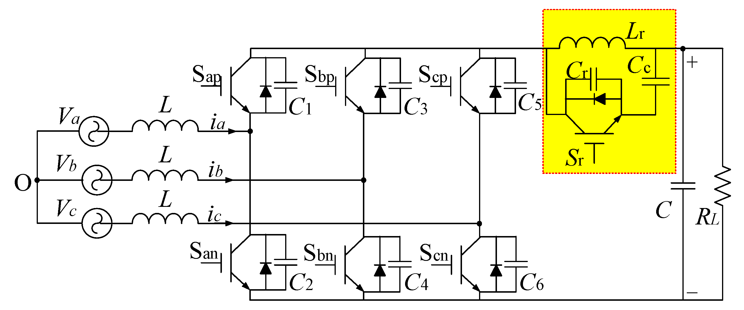
The compound active-clamping ZVS three-phase PFC rectifier is shown in
Figure 1. Within the dotted wire frame is the auxiliary circuit of the main and auxiliary switches to realize soft switching.
The rectifier is a standard six-switch, three-phase boost PFC with an added auxiliary circuit, which includes an auxiliary switch Sr, a clamp capacitor Cc, and a resonant inductor Lr. The working frequency of the auxiliary switch is the same as that of the main switches. The switching frequency of the converter is fixed. With a one-cycle control strategy, all the main and auxiliary switches can be zero-voltage switched, and the switches have low voltage stress. The reverse recovery current of the switch reverse parallel diode is also suppressed.
The three-phase, six-switch rectifier controlled by conventional SPWM or SVM requires six current commutations in one operating cycle. If the bridge arm switch with the largest phase current is not operated, the four current commutations will occur in one switching cycle, two of which are the reverse parallel diode commutating to the opposite switch, and the other two are the switches commutating to the opposite reverse parallel diode. The former two are natural soft switches, while the latter two are hard switches, and the reverse recovery of the diode exists.
In a compound active clamp converter, the auxiliary switch operates only once during a period of the main switch’s operation, resonates the DC bus to zero, and creates the condition of a zero voltage switch for the main switches. The switching of two main switches with reverse recovery must be completed in this zero voltage time. This paper presents an improved one-cycle control method which can realize this process.
3. One Cycle Controller
In this part, the traditional one-cycle control [
21] is briefly introduced, and the process of the main bridge arm switch is analyzed. On this basis, an improved one-cycle control method is proposed, and the detailed process of realizing the soft-switching action of the active clamp ZVS three-phase rectifier circuit in
Figure 1 is analyzed.
3.1. One Cycle Controller for Three-Phase PFC Rectifier
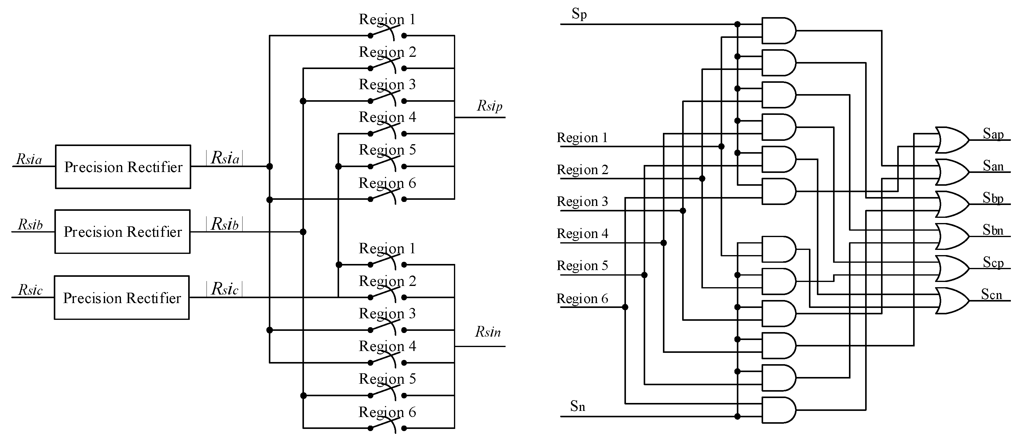
The three-phase voltage is divided into six regions in a cycle, each of which is 60° as shown in
Figure 2. The polarity of the phase with the largest voltage is always opposite to that of the other two phases. Therefore, only two phase currents with the same polarity need to be controlled in each region. Due to the fact that sum of three phase currents without the middle line equals zero, the third phase will be controlled after controlling two phases.
In the first region [0°, 60°], the three-phase control can be realized by controlling the switches S
an and S
cn in
Figure 1. The equivalent duty cycles are given by
where
dxx denotes the duty cycle of S
xx.
According to reference [
21], the parameter
Vm is defined as
where
Rs is the equivalent resistance of current detection and
Re is the equivalent input resistance of rectifier.
So the one-cycle control equation can be obtained as follows
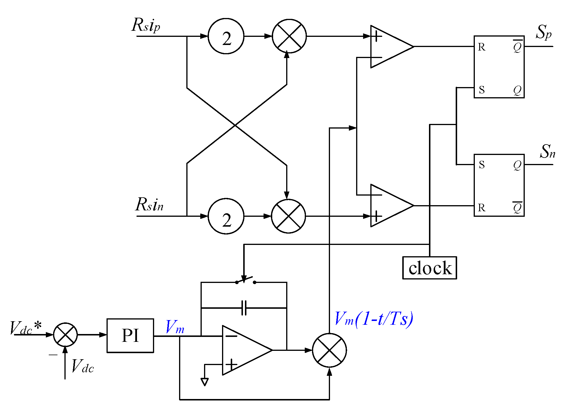
According to Formula (3), the core control circuit of the one-cycle controller can be obtained as shown in
Figure 3.
For different control regions, ip and in are different, which can be any two of the currents ia, ib and ic. Similarly, the switches corresponding to Sp and Sn have different choices in different control regions.
The purpose of a one-cycle control can be achieved by selecting the input and output signals of the control circuit in
Figure 3 from the output region signals of the partition circuit in
Figure 4. The input selection circuit and output driving signal of the controller is shown in
Figure 5.
Combining
Figure 3,
Figure 4, and
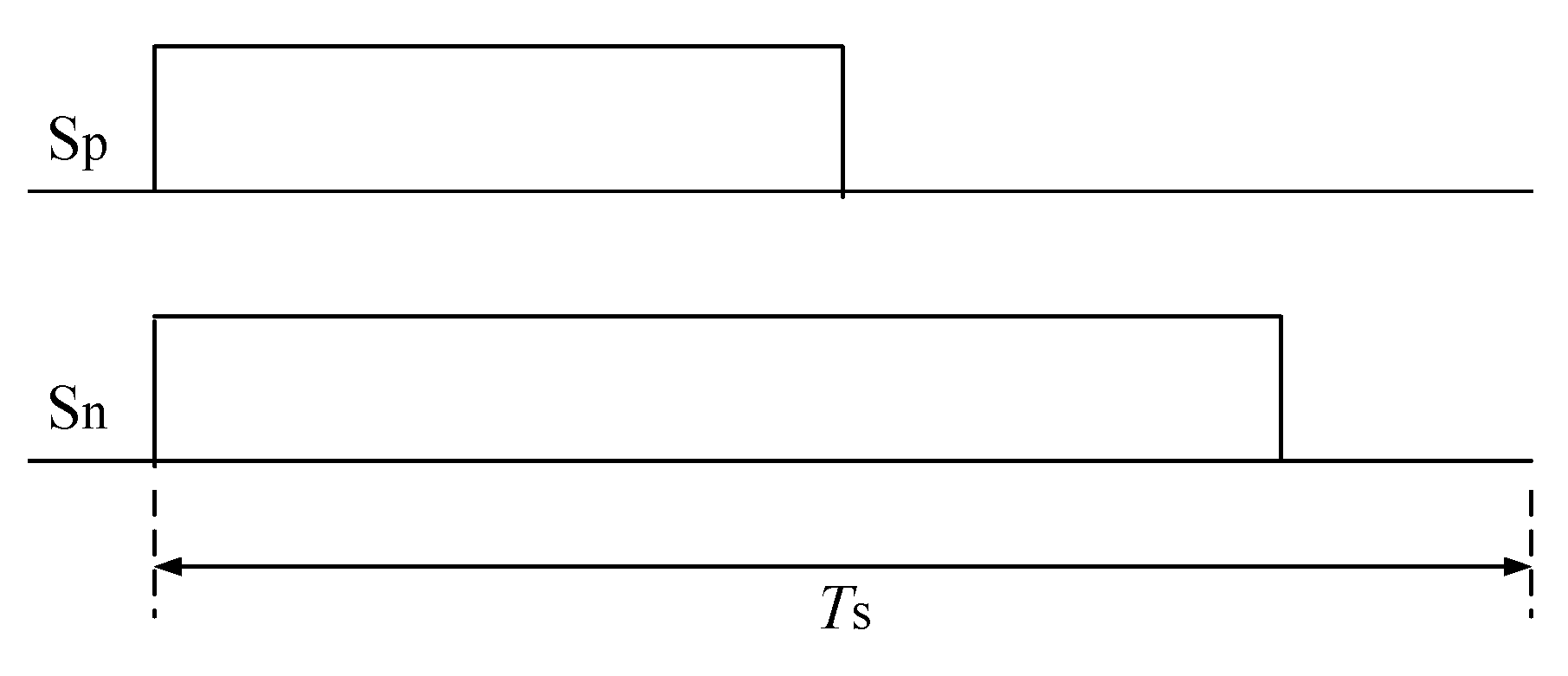
Figure 5, a three-phase six-switch PFC rectifier one-cycle controller is formed. In each control cycle, only two of the six switches have switching operations while the other four switches are in no-operation and are acted by a reverse parallel diode. The two switches that participate in the action of the switch are always turned on at the same time at first. After a period of time, the two switches are closed successively, as shown in
Figure 6.
The sequence of closing two action switches is determined by the working region, and the two switches involved in operation are either both upper arm or lower arm at the same time, so there will not be a case where one is in upper arm and the other is in lower arm. In each working region, the operation mode of the switches participating in the switching action is the same. In a switch cycle, each bridge arm has one current commutation. When the switch is turned off, it is a soft switch, and when the switch is reset and turned on, it is a hard switch. For soft switching when the switch is reset and turned on, it is necessary to make amends to the one-cycle control, as illustrated above.
3.2. The Proposed One Cycle Controller
The one-cycle controlled ZVS three-phase compound active clamp rectifier requires the main switches and the auxiliary switch to work at the same frequency. The auxiliary switch is always turned off before the main switches turn on in all situations. At this time, the auxiliary resonant inductance current discharges the parallel capacitors of the main switches to make the arm’s volt resonate to zero and then turn on the main switches. The purpose of this is to realize zero-voltage turn-on. In addition, due to the existence of auxiliary resonant inductance, the reverse recovery characteristics of the switch diode in parallel are suppressed. The driving waveform of the auxiliary switch S
r is characterized by turning off before the two control switches S
n and S
p turn on, and turning on before the two control switches S
n and S
p turn off. The improved one-cycle control does not need to change the original control circuit, but only needs to process the clock reset signal of the one-cycle control to obtain the driving signal of the auxiliary switch, as shown in
Figure 7.
The method of processing is to get two delays tds for clock signal, and obtain the signals clk1 and clk2 respectively. Then, the two signals of clk1 and clk2 are processed to obtain the driving signal of the auxiliary switch Sr. Finally, the driving signal of Sr is anti-compressed to obtain the clk_set signal, which is used as the reset clock signal of the one-cycle core control circuit. The selection choice for the clock circuit is flexible, and can include circuits such as the crystal oscillator circuit or a clock pulse generator composed of 555 timers. For the delay circuit, the simplest method is to use an RC charging and discharging circuit and shape the waveform through a logic gate circuit. For the compression process of fetching Sr, the driving signal, a simple delay circuit adds an AND gate can be used. The process described above can also be implemented by programmable logic devices.
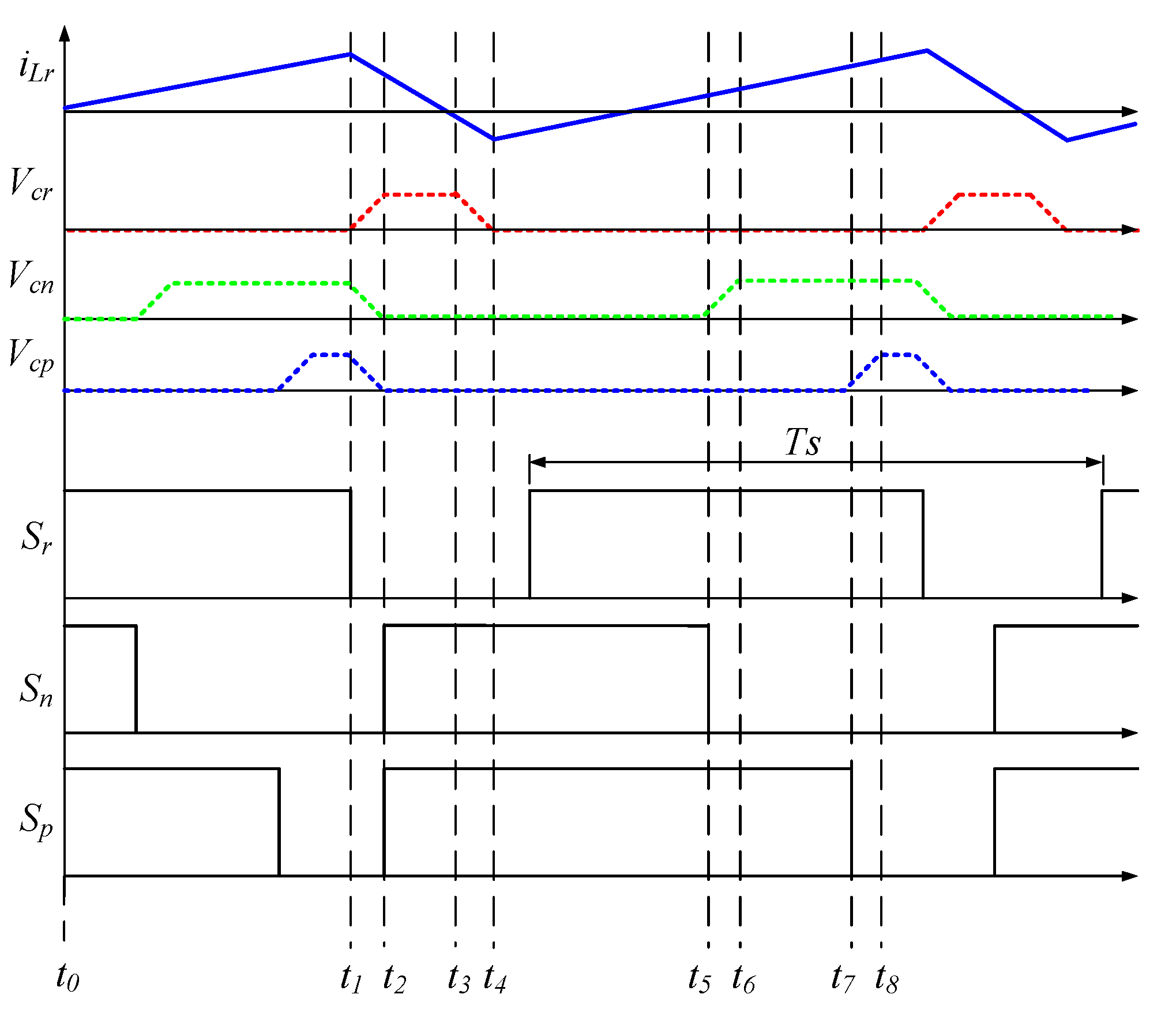
The specific working waveform of the three-phase active clamp PFC rectifier soft switch is shown in
Figure 8.
The saw-tooth wave is the current waveform iLr of the resonant inductance. The three dotted lines are voltages of the two main switches Vcn, Vcp and one auxiliary switch Vcr. From the waveform, it can be inferred that the three switches are all turned on when the voltage is zero, thus achieving the goal of zero voltage conduction. Because each switch has a parallel capacitor, the zero voltage turning off of the switch is guaranteed. Therefore, all switches are zero voltage action, and the whole circuit achieves soft switching.
3.3. Operating Modes over a Switching Cycle
In any working region, the corresponding equivalent rectifier circuit is shown in
Figure 9.
In the second half of the first region [30°, 60°], the currents of phases a and c are positive and the current of phase b is negative. At this region, it is then known that
Figure 9 corresponds to
Figure 1.
Vp =
Vab,
Vn =
Vcb,
Lp =
Ln=
Lt =
L, D
t is S
bn’s parallel diode, S
n and C
n are S
cn with its parallel capacitor, D
n and C
5 equivalent to S
cp’s parallel diode and capacitor, and S
p and C
p are San with its parallel capacitor, D
p and C
1 equivalent to Sap parallel diode and capacitor.
From
Figure 8, it can be seen that there are eight operating modes in the circuit of
Figure 9 in one switching cycle. Taking the first working region as an example, eight working modes are analyzed one by one.
3.3.1. Mode 1: (t0–t1)
All the main switches are turned off and the auxiliary switches S
r is turned on. In the first region, the currents of phases A and C are positive, and the phase B current is negative, so the reverse parallel diodes D
p, D
n, and D
t are turned on. In the resonant groove circuit consisting of auxiliary resonant inductor
Lr, clamping capacitor
Cc and auxiliary switch S
r, the voltage of auxiliary resonant inductor
Lr is the clamping capacitor voltage
VCc, and the current of resonant inductor increases linearly with the current change rate
At t = t1, the auxiliary switch Sr turns off, and this mode ends.
3.3.2. Mode 2: (t1–t2)
At t = t1, the auxiliary switch is turned off and the auxiliary inductance current begins to decrease. The auxiliary inductance Lr resonates with capacitors Cr, C3, Cn, and Cp. Lr causes C3, Cn, and Cp to discharge and charges Cr. Because of the existence of Cr, the auxiliary switch Sr reaches zero voltage and turns off. At t = t2, the voltage of the three main switches Sn, Sp, and Sbp and the parallel capacitors Cn, Cp, and C3 drops to zero and the resonance stops, and this mode ends.
3.3.3. Mode 3: (t2–t3)
At
t =
t2, S
n and S
p parallel diodes start to turn on. After that, D
n and D
p diodes begin to enter the reverse recovery stage. The auxiliary inductance current continues to decrease with the relation depicted below:
The duration of this mode is very short, which is the reverse recovery time of Dn and Dp diodes on the bridge arm.
3.3.4. Mode 4: (t3–t4)
At t = t3, when the Dn and Dp diodes are completely turned off, the auxiliary resonant inductance current is zero. Thereafter, the auxiliary resonant inductor Lr and capacitors C1, C3, C5, and Cr begin to resonate again. The voltages of C1, C3, and C5 begin to rise and the voltages of Cr start to decrease. At t = t4, the voltage of C1, C3, and C5 rises to Vo + VCc and auxiliary switch Sr has a voltage of zero. Sr is parallel to the diode clamp, causing resonance stop.
3.3.5. Mode 5: (t4–t5)
At
t =
t4, the current of the auxiliary inductor reaches the maximum negative polarity and begins increasing in polarity. The current of the auxiliary inductor rises linearly with the rate of change given by
3.3.6. Mode 6: (t5–t6)
At t = t5, the main switch Sp is turned off, the input boost inductor charges Cp and discharges C1. Because of the existence of capacitor Cp, Sp achieves zero-voltage turn-off.
3.3.7. Mode 7: (t6–t7)
At
t =
t6, when D
p is turned on, the auxiliary resonant inductor
Lr voltage is clamped on capacitor voltage
VCc, and the auxiliary inductor current rate of change is as follows
3.3.8. Mode 8: (t7–t8)
At t = t7, the main switch Sn is turned off, the input boost inductor charges Cn and discharges C5. Because of the existence of the capacitor Cn, Sn achieves zero-voltage turn-off. At t = t8, Dn is turned on and then the entire process repeats from Mode 1.
5. Discussion
The compound clamp ZVS three-phase VSR circuit mentioned in reference [
19,
20,
21], achieves ZVS in all switches, including auxiliary switches. The auxiliary circuit is simple and the additional system has a low extra loss. However, the ZVSSVM controller must be implemented by intelligent chips such as DSP, which is complex and difficult to popularize. The governing equation of the one cycle controller, which is derived based on the input current following the change of input voltage, determines the ability of the system to control the power factor close to 1 [
22,
23,
24,
25,
26,
27,
28]. This paper adjusts and improves the original one cycle control strategy, by adding the driving signal of an auxiliary switch, which can complete the ZVS control of the compound clamp ZVS three-phase VSR circuit. Although only two switches on the main bridge arm are controlled, the conducting form of the third switch is replaced by the diode conducting in parallel with that switch. The improved one cycle control proposed in this paper share many similarities with the ZVSSVM control strategy in reference [
19,
20,
21]. The major difference between the two systems stems from the use of ordinary circuits in the proposed technique to avoid complex computation used by the intelligent chip in ZVSSVM control strategy which needs to sample the voltage and current sensor signals and carry out multiple multiplications nonlinear operations to obtain the driving switch signals. There is a certain delay time in the process of data sample and calculation. The nonlinear multiplication operation brings calculation errors, and its anti-interference ability is not good enough. Due to the avoidance of complex calculation of the intelligent chip, the proposed system has better performance on real-time applications and stability.
Formula (2) indicates that the input impedance has become a factor in the signal Vm rather than an estimated parameter. When the load changes, the input impedance also changes at the same time, then quickly reflects the signal Vm, and duty cycle adjustment is immediately started within the current control cycle. Therefore, different from traditional converter, the control system proposed in this paper has adaptive capability for input and output impedance. The proposed control algorithm is similar to the flat top SVM modulation method, so it can work at higher switching frequencies. In the denominator of the formula for calculating the pulse width of the flat-top SVM, there is a DC link voltage value factor, and the voltage pulsation of the dc link has a great disturbance to the PWM duty ratio, thus affecting the output voltage. Meanwhile, the duty cycle proposed in this paper is only related to the average input and output current after the equivalent transformation of Equation (3), which is also the reason why it is adaptive to the load.
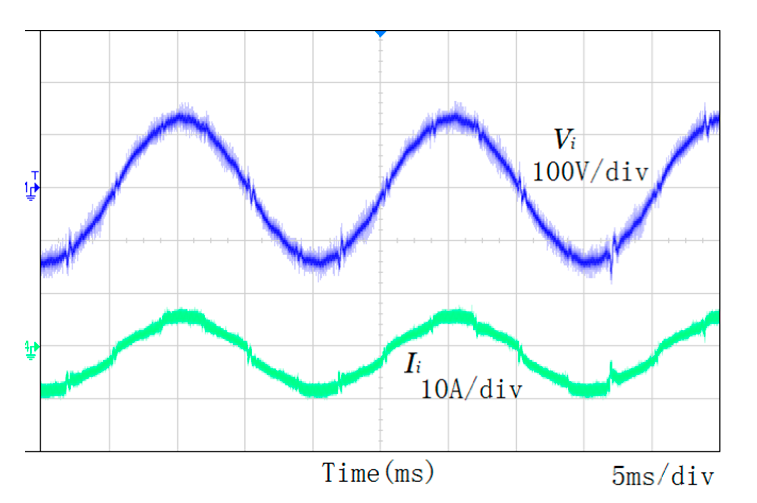
This controller requires synchronous switching between the interval signal and the drive signal. Otherwise, the input currents will have a large current pulse overshoot, which may destroy the switches under high power output. In this paper, the drive signals (S
n and S
p) are switched synchronously by the clock signal trigging, such that the input current waveform will not have large disturbance, as shown in
Figure 16. In addition, the optimization design of relevant resonance parameters of this method can only be adjusted empirically, and there is no strict theoretical basis, which is the arrangement of the next research work.


