1. Introduction
The concept of modular voltage source inverters (VSI) with coupled reactors considered in this paper was first reported in [
1] (therein dubbed multipulse voltage source converters (VSC) with coupled reactors). The idea has its roots in the well-known multipulse AC–DC converter topologies widely used in a variety of applications, including adjustable speed drives (ASD), high-voltage direct current transmission (HVDC), aircraft power systems, and renewable energy conversion systems [
2,
3,
4,
5]. The use of multipulse topologies for the DC–AC power conversion has broad coverage in the literature (see, for example, in [
6,
7,
8,
9,
10,
11]). The topologies proposed in [
8,
9,
10,
11] are based on the use of a transformer in an integrating circuit, which significantly increases the size of the device and is an expensive solution. If the application does not require galvanic isolation of the DC side from the AC side, the integrated circuit can be based on coupled reactors, as proposed in [
1]—a solution which greatly reduces the size and cost of the circuit.
Solutions presented in [
1,
7,
8,
9,
10,
11] are focused on maximizing the achievable magnitude of output voltage, while the control of lower magnitudes is left out. The possible voltage synthesis using all allowed combinations of switch states has not been seriously addressed so far. In this paper, a control of the output voltage of the modular voltage source inverters proposed in [
1,
12] is considered. These converters contain standard inverter modules, but they are connected by special coupled reactors. The idea of modular VSI with coupled reactors draws on the properties of multipulse diode rectifiers with similar coupled reactors [
13,
14,
15] and other converters with integrating magnetic circuits [
4,
16,
17]. Coupled reactors were selected as integrating elements because their rated power is below 20% of that of a transformer with similar integrating properties [
5,
13,
14]. As the inverter modules are connected in parallel, these circuits can be used for high-current systems. Where increased operating voltages are required, multilevel inverters can be used as modules.
To clarify the terminology used in the sequel, note that the idea of “pulses” contained in the term “multipulse” has a simple interpretation in the case of diode or thyristor AC–DC converters: it denotes a section of AC input voltage transferred to the DC output. The “number of pulses”, denoted M, is used to mean the number of such sections transferred in one fundamental period of the AC voltage. Although for DC–AC inverters with fully controlled power switches this idea of pulses is much less tangible, the number of pulses can still be used for the sake of discussion—as a constructional parameter of the inverter.
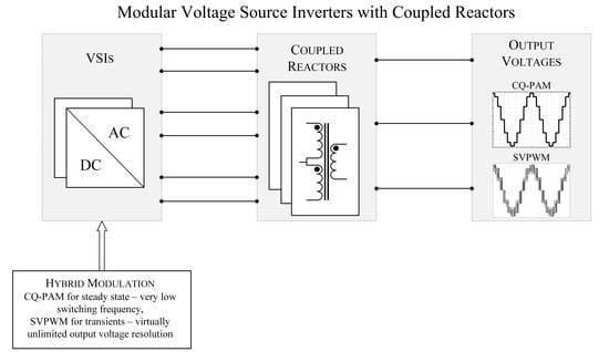
Transistor-based modular VSI with coupled reactors can be controlled in a variety of ways. One of the methods mimics the workings of multipulse rectifiers. This method relies on applying a succession of only M inverter voltage vectors in every fundamental period of the synthesized output voltage. This paper demonstrates that by appropriate selection of all available basic voltage vectors, it is possible to achieve coarsely quantized pulse amplitude modulation (CQ-PAM). This control approach, leading to staircase output voltage waveforms, enjoys very low switching frequency of power transistors (equal to the fundamental frequency of the output voltage). A drawback of this modulation method is low amplitude resolution. A workaround might be application of a controlled source of DC voltage, but this option is complex and costly and thus it is left out in this paper.
High-resolution voltage control can be achieved by means of pulse width modulation (PWM). Unlike CQ-PAM, PWM requires relatively high switching frequency (a multiple of the fundamental frequency of output voltage), which can be particularly disadvantageous in high-speed motor drive applications. For example, a two-pole motor operating at 150,000 rpm would call for 5 kHz fundamental frequency of the output voltage, meaning at least several dozens of kilohertz of the transistor switching frequency for PWM controlled inverter. Such high switching frequencies can cause significant mismatches between the transistor on/off commands and the actual turn-on/turn-off timing. What is more, the switching losses and electromagnetic interference resulting from high switching frequency can be prohibitive [
18]. The problem of adequate voltage control increases with the increase of motor speed and/or its power. For instance, motor drives in the 1 kW power range are reported to operate at speeds of 500,000 to 1,000,000 rpm [
19,
20]. Concerning higher power drives, the authors of [
21] report on a 60 kW drive operating at 100,000 rpm, while the authors of [
22] describe a 300 kW drive operating at 60,000 rpm.
To address the above problems, this paper proposes a hybrid modulation combining CQ-PAM and PWM. This approach is capable of combining advantages of PWM (virtually unlimited resolution of voltage control) and those of CQ-PAM (radically reduced switching frequency). The CQ-PAM is intended for use at steady state, while the PWM ensures smooth passage through the transients. A somewhat similar idea of hybrid modulation was proposed in [
23,
24], but it relies on a combination of two different PWM methods: space-vector pulse width modulation (SVPWM) is used for smooth transients, while selective harmonic elimination PWM (SHE-PWM) is applied for low switching frequency operation at steady state. The CQ-PAM proposed here is even more effective in the reduction of switching frequency than SHE-PWM and—unlike the latter—can easily be computed in real-time. Both CQ-PAM and PWM can rely on selecting and applying appropriate voltage vectors. At steady state, a succession of only
M different vectors per fundamental period is used for
M-pulse inverters, with all vectors being applied for time intervals of the same length. At each interval, the voltage vector closest to the reference vector is selected. Concerning the PWM, vector selection and duty cycle computations are carried out using the barycentric coordinates [
25]. This approach speeds up the calculations and allows easy inclusion of the DC link voltage fluctuations in the algorithm. The proposed modulation is exposed and discussed using the simplest case of modular VSI, that is, a 12-pulse inverter with two-level component inverter modules. The application of the proposed approach can easily be extended to inverters with higher pulse numbers and/or with multilevel inverter modules [
1,
12].
Section 2 derives the formula linking the output voltage of modular VSI with coupled reactors with the voltages supplied by component inverter modules and finds the required turns ratio of the coupled reactors.
Section 3 presents the proposed modulation method, while
Section 4 presents and discusses selected simulation results pertaining to modular VSI using two-level and three-level component inverters and the CQ-PAM. A simulation of the passage between two different steady states using the proposed SVPWM is also demonstrated. The laboratory test results of the same two topologies are presented in
Section 5.
2. The 12-Pulse Modular Voltage Source Inverter with Coupled Reactors
Twelve-pulse topology has been known as early as in the 1980s [
14,
26] and widely used in industry to date [
5,
27,
28,
29]. However, the first attempts to use this topology (with coupled reactors) in the inverter mode of operation were made only several years ago [
1,
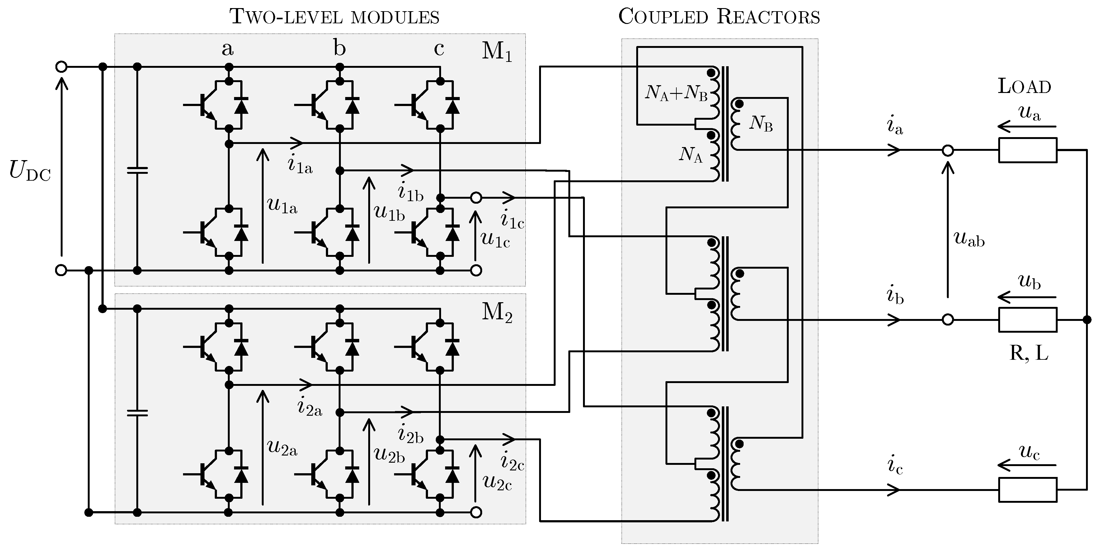
7]. To the best of the authors’ knowledge, there have been no other reports on the use of multipulse topologies for DC–AC conversion. This section analyses the output voltage of the considered modular VSI as a result of vector summation of the component inverter voltages and determines the required turns ratio of the coupled reactors. A schematic diagram of the 12-pulse modular VSI with coupled reactors is shown in
Figure 1, while
Figure 2 establishes vectorial notation of voltages used in the following analysis.
According to the diagram in
Figure 2, the output voltage vector of the analyzed modular VSI is given by
where
Thus, on the basis of Equations (
1)–(
3), the output voltage can be described by
After simple algebra, Equation (
6) can be rewritten as
It is assumed that the control signals of the inverter modules in the considered 12–pulse system are phase-shifted by
, meaning the same phase shift between vectors
and
. As a result, Equation (
7) can be converted to
In order to determine the appropriate turns ratios of the reactor coils, assume that the magnitude of voltage across a coil is proportional to its number of turns. Then, from
Figure 2 it immediately follows that
The desirable turns ratio is such that ensures symmetric contribution of the component voltages
and
to the output voltage
, as illustrated in
Figure 3. From the vector diagram in
Figure 4, which is an enlargement of the shaded fragment in
Figure 3, the following relationship can be found using Thales’s theorem,
where
. Now, using this value of
and substituting Equation (
10) to Equation (
9), one arrives at
whereupon, using basic trigonometric relationships, an explicit formula for the required turns ratio of the reactor coils is found:
3. Proposed Hybrid Modulation Method
In one of the proposed operation modes of the considered modular VSI, transistors of inverter modules commute with the fundamental output frequency, which means significant reduction of switching losses and electromagnetic interference (EMI) distortion, and allows high frequencies of output voltages. The problem with this type of control, referred to as the CQ-PAM, is the limited resolution of the output voltage. The proposed solution is the use of PWM as a complementary control method. Both modulation techniques are based on appropriate selection and timing of the available basic vectors, that is, voltage vectors corresponding directly to the on/off states of inverter switches. These vectors can be considered points on a two dimensional
plane. The basic vector diagram for the considered 12-pulse system is shown in
Figure 5a. The basic vectors in
Figure 5 are obtained in two steps. First, the leg voltages of component inverter modules (marked in
Figure 1) are transformed to phase voltages of the modular VSI by
where
Then, the
coordinates of the corresponding basic vectors
are determined by the Clarke transformation:
In general, the number of different basic vectors for an M-pulse inverter with l-level inverter modules is . Therefore, the considered 12-pulse converter exhibits 64 different basic vectors.
3.1. Coarsely Quantized Pulse Amplitude Modulation (CQ-PAM)
Basically, the CQ-PAM involves applying a succession of only
M different basic vectors per fundamental period, with all vectors having the same magnitude and being applied for equal-length time intervals. The selection of basic vectors relies on the criterion of proximity between the reference vector and the basic vectors. As seen in
Figure 5a, for
and
only four different non-zero magnitudes are available, meaning very limited resolution. However, as can be noticed in
Figure 5b,c, as the number of inverter modules or inverter voltage levels increases, the resolution of the CQ-PAM significantly rises—for an 18-pulse modular VSI it is 16 magnitudes and for a 12-pulse modular VSI with three-level modules it is 24 magnitudes.
For increased
M and/or
l, some neighboring magnitudes are close to each other, and thus it can be beneficial to use their combinations rather than stick to the same-magnitude principle. This option is illustrated in
Figure 5b for the 12-pulse VSI with three-level modules: the sequence of vectors leading to the waveform shown in the lower graph is a succession of 24 (that is,
) basic vectors indicated in the upper graph; the magnitude of the shorter vectors is
times that of the longer vectors. What is more, some magnitudes can be represented by more than
M vectors. For instance, the 12-pulse VSI with three-level modules has seven magnitudes represented by
basic vectors. Again, this fact can be exploited in the CQ-PAM algorithm.
3.2. Space Vector Pulse Width Modulation (SVPWM)
To ensure virtually unlimited amplitude resolution of output voltage control, the PWM can be used whenever necessary or desirable. An economic solution might be the PWM discussed in [
17,
30] for 12-pulse rectifiers. However, this PWM technique offers only limited voltage control range and does not take advantage of the natural elimination of low harmonics in multipulse systems. Another candidate solution might be selective harmonic elimination PWM (SHE-PWM), which allows to decrease the switching frequency and remove a set of selected harmonics. Such a method was applied for parallel inverters driving a single load separated by line reactors [
31]. However, this method requires precomputation of the appropriate PWM patterns, which is hardly possible in real-time [
32,
33]. This paper proposes an innovative space-vector PWM (SVPWM) based on barycentric coordinates.
In most cases considered in the literature, the output vectors are synthesized using the nearest three vectors (NTV) approach. A similar approach is adopted in this paper. In order to select the nearest basic vectors, the magnitude of reference vector
is compared with the available magnitudes of inverter basic vectors. The comparisons permit determining two neighboring magnitudes between which the reference vector is located. The closest two basic vectors of either magnitude are then searched for using a simple sorting algorithm and the following vector distance relationship
The so obtained closest vectors can be considered vertices of a quadrangle ABCD, as illustrated in
Figure 6. The quadrangle can be divided into four triangles. The tasks of the modulation include selecting the most appropriate of the triangles and computing the duty cycles of the three corresponding basic vectors.
Both of the above indicated tasks can be achieved with the aid of barycentric coordinates [
25]. Unlike the most popular methods of PWM computations, which are based on trigonometric functions, the use of barycentric coordinates avoids the related inconvenience. Consider the reference vector in
Figure 6. It can be considered a point inside triangle ABC or triangle ACD. To fix attention, let us focus on the former triangle. The computation of duty cycles of the corresponding basic vectors is effectively means expressing the position of the reference vector as a linear combination of basic vectors. This is equivalent to expressing the Cartesian coordinates of a point inside a triangle by the barycentric coordinates of that point. Thus, the coordinates of vector
in
Figure 6 can be expressed by the coordinates of points A, B, and C:
where
,
, and
are the barycentric coordinates of
, which can be calculated from
with the
symbols representing the areas of the small triangles defined inside triangle ABC by the vertices of the latter and
. Stated differently, the barycentric coordinates are equal to the normalized areas of their corresponding small triangles. These areas can be computed direct from the
coordinates of the appropriate basic vectors by
A useful property of the barycentric coordinates is that their sum is equal to unity if they are calculated for a point inside a triangle (e.g.,
in the triangle ABC or ACD in
Figure 6), but is greater if the point lies outside the triangle (e.g.,
in the triangle ABD or BCD in
Figure 6). Thus, a uniform and effective method of finding a triangle or triangles containing a reference vector may be to calculate some candidate barycentric coordinates and then select the smallest (ideally 1).
As can be seen in
Figure 6, the reference vector can be located inside two different triangles, and so some additional selection criterion is necessary to make the choice unique. The proposed algorithm selects the triangle for which the distance between the reference vector and the centroid
is smaller. This criterion was adopted in order to minimize the occurrence of narrow pulses. The coordinates of the centroids are calculated as arithmetic means of the coordinates of vertices:
The distance between
and the centroids is determined by Equation (
16).
Although the proposed computational approach may seem rather complex for a system with only 64 space vectors, the practical target for the proposed method is modular VSI inverters with higher number of pulses
M (notably, 18- and 24-pulse circuits) and using multilevel component inverters [
1]. For such systems, the number of basic space vectors increases rapidly with
M and the number of inverter levels (see
Figure 5), as shown in
Table 1.
It is also important to note that with the increasing number of pulses and levels, the number of available magnitudes of inverter basic vectors also increases rapidly (e.g., 18-pulse and 24-pulse inverters with two-level modules have 16 and 67 output voltage magnitudes respectively and 12-pulse modular VSI with three-level modules has 23 output voltage magnitudes), rendering the CQ-PAM mode a true alternative to the PWM for steady-state operation, with the proposed SVPWM becoming a method for increasing the voltage control resolution, especially during transients.
3.3. Selection of Modulation Method
The selection between CQ-PAM and SVPWM can be based on a variety of criteria, depending on the application (for instance the frequency criterion: SVPWM to be selected for lower fundamental frequencies, e.g., during the start-up, and CQ-PAM for higher fundamental frequencies). For the purpose of this study, the following magnitude proximity criterion is used; CQ-PAM is selected if the reference vector lies inside an annulus
defined by two circles—one inscribed in and the other described on a certain
M-gon made of vectors of the
magnitude (
); otherwise, SVPWM is chosen.
The selection of the modulation method can be based on a decision diagram shown in
Figure 7.
4. Simulation Results
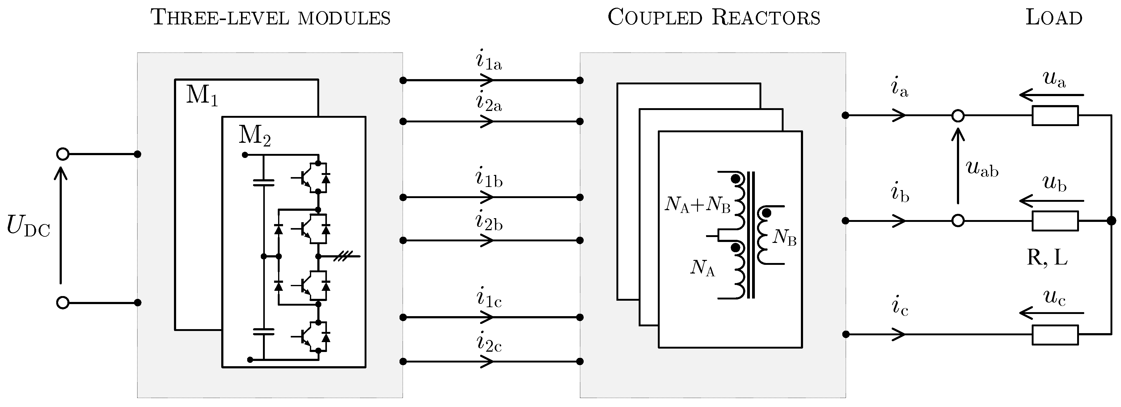
The proposed concept of output voltage control for modular VSI with coupled reactors has been verified using the PSIM11 simulation software and the Matlab environment. The simulated topologies included the 12-pulse inverter with two-level modules (
Figure 1) and the 12-pulse inverter with three-level modules (
Figure 8). The most important circuit and control parameters are given in
Table 2.
The operation of the considered modular VSI with CQ-PAM is illustrated in
Figure 9. Characteristic values for output voltages and currents for this control mode are given in
Table 3. A comparison of output voltage and current waveforms for two-level and three-level inverter modules is shown in
Figure 10. To demonstrate how low the switching frequency is in relation to the output voltage frequency, the above figure also visualizes the leg voltage
waveform (scaled down to 25% in
Figure 9 and
Figure 10). The output voltages shown in
Figure 9 are the time waveforms corresponding to 12-pulse space-vector diagrams presented in
Figure 5a. Later in this section a passage is illustrated between two steady-state operating points with the aid of SVPWM invoked during the transients (
Figure 11).
Figure 10 illustrates the maximum-magnitude and minimum-magnitude output voltages of 12-pulse modular VSIs with two-level and three-level modules, and the corresponding currents and leg voltages. As can be seen, the use of multilevel modules can increase the number of output voltage steps, so that the total harmonic distortion (THD) of the output voltage decreases (from
for two-level modules to
for three-level modules), and so does the THD of output currents (from
to
respectively). Moreover, for multilevel modules the dynamic range and resolution of output voltage magnitudes increases compared to the two-level modules. The minimum voltage for modular VSI with three-level modules is about four times lower than for two-level modules. The number of available non-zero voltage magnitudes also increases—from four in the case of two-level modules to twenty-three for three-level modules.
Figure 11 illustrates combined use of the proposed SVPWM and the CQ-PAM, ensuring smooth passage between different steady states. In this particular example the passage is between steady states at
and
.
5. Laboratory Test Results
The laboratory tests have been performed using two prototypes of modular VSI with coupled reactors: one using two-level inverter modules, and the other equipped with three-level modules. The laboratory setup is presented in
Figure 12. The most important circuit and control parameters are the same in both cases and identical to those used in the simulation (cf.
Table 2). Measurements were taken by a Tektronix MDO4104B–3 oscilloscope. The control board contained a the two-core Texas Instruments digital signal processor TMS320C6672 and an Intel programmable logic device CYCLONE V. The coupled reactors shown in
Figure 12 were designed for 30 kW (10 kW each) and rated frequency of 2.5 kHz. The numbers of turns of reactor coils are given in
Table 2.
Figure 13 illustrates output phase voltages and currents, component inverter leg voltages, and the voltage across coil
for all output voltage magnitudes and parameters listed in
Table 2 (for CQ-PAM controlled VSI with two-level modules). The waveforms correspond to the simulation results shown in
Figure 9. The laboratory test results match the results of the simulation, except for the voltage spikes appearing between the steps in the laboratory waveforms. This is a consequence of the use of dead time and the fact that several inverter legs are switched simultaneously (for voltage magnitudes other than the maximum one). However, it can be noted that the amplitudes of these spikes are not significant (smaller than
) and do not noticeably affect the current waveforms. The inverter leg voltages indicate the frequency with which the power switches commute (the waveforms confirm the data in
Table 3). For the maximum available output voltage the switching frequency is equal to the fundamental output voltage frequency (in this case 1 kHz), and for the smallest CQ-PAM controlled output voltage it is equal to five times the output voltage frequency (5 kHz). One of the most important features distinguishing the coupled reactors from other magnetic integrating elements is their low rated power (related to the power of the overall system). To illustrate this feature,
Figure 13 shows the voltage across the
coil of the coupling reactor. The voltage is not only significantly lower than
, but may even assume values close to zero for some steps (depending on the output voltage magnitude). Therefore, the power transmitted through the reactor is only a fraction of the rated power of the inverter.
The hybrid modulation discussed in
Section 3 is based on a combination of the CQ-PAM specific to the considered topologies, and the universal SVPWM—using the proposed computational approach based on barycentric coordinates.
Figure 14 illustrates the phase voltages as well as phase-to-phase voltages for both modulation strategies. The voltages in
Figure 14 correspond to
for CQ-PAM, and
for SVPWM.
Figure 15 shows the voltages and currents obtained by SVPWM for two operating points:
and
. The fundamental frequency was 1000 Hz for the higher output voltage and 600 Hz for the lower.
The quality of output voltage and current will improve significantly with the increase in the number of inverter levels, as exemplified in
Figure 16 and
Figure 17, which provide an initial comparison between the modular VSIs with two-level and three-level inverter modules. What is more, increasing the number of levels significantly increases the amplitude resolution of the CQ-PAM and reduces the voltage stresses of individual transistors. Consequently, the use of multilevel component inverters in the modular VSIs with coupled reactors will contribute to increased attractiveness of the considered topology.
The modularity of the considered topology is an important advantage in itself. It allows, inter alia, even distribution of the overall power transferred by the inverter between the reduced-power modules. This feature is illustrated in
Figure 18, which shows the phase currents of the component inverters (
,
) and the resultant load currents (
). As can be seen, the component inverter currents have the same amplitude close to half of the load current. The modularity also improves operational reliability of the considered topology, because it can continue working in case of a failure of one component inverter.

 ,
, 


