Article

Design of Silicon Nanowire Array for PEDOT:PSS-Silicon Nanowire-Based Hybrid Solar Cell

by
Syed Abdul Moiz
1,*,
A. N. M. Alahmadi
1 and
Abdulah Jeza Aljohani
2,3
1
Department of Electrical Engineering, Umm Al Qura University, 21955 Makkah, Saudi Arabia
2
Department of Electrical and Computer Engineering, King Abdulaziz University, 21589 Jeddah, Saudi Arabia
3
Center of Excellence in Intelligent Engineering Systems (CEIES), King Abdulaziz University, 21589 Jeddah, Saudi Arabia
*
Author to whom correspondence should be addressed.
Energies 2020, 13(15), 3797; https://doi.org/10.3390/en13153797
Submission received: 3 July 2020 / Revised: 20 July 2020 / Accepted: 20 July 2020 / Published: 24 July 2020
(This article belongs to the Special Issue Nano-Structured Solar Cells 2020-2022)

Abstract

:
Among various photovoltaic devices, the poly 3, 4-ethylenedioxythiophene:poly styrenesulfonate (PEDOT:PSS) and silicon nanowire (SiNW)-based hybrid solar cell is getting momentum for the next generation solar cell. Although, the power-conversion efficiency of the PEDOT:PSS–SiNW hybrid solar cell has already been reported above 13% by many researchers, it is still at a primitive stage and requires comprehensive research and developments. When SiNWs interact with conjugate polymer PEDOT:PSS, the various aspects of SiNW array are required to optimize for high efficiency hybrid solar cell. Therefore, the designing of silicon nanowire (SiNW) array is a crucial aspect for an efficient PEDOT:PSS–SiNW hybrid solar cell, where PEDOT:PSS plays a role as a conductor with an transparent optical window just-like as metal-semiconductor Schottky solar cell. This short review mainly focuses on the current research trends for the general, electrical, optical and photovoltaic design issues associated with SiNW array for PEDOT:PSS–SiNW hybrid solar cells. The foremost features including the morphology, surface traps, doping of SiNW, which limit the efficiency of the PEDOT:PSS–SiNW hybrid solar cell, will be addressed and reviewed. Finally, the SiNW design issues for boosting up the fill-factor, short-circuit current and open-circuit voltage will be highlighted and discussed.

1. Introduction

We are living in the era of industrialization, which requires s huge amount of energy and any technological advancement ultimately raises our standard of living and requires more energy. In order to fulfill the ever-rising demand of energy, the current fossil fuel resources are sharply depleting and will not be sufficient to maintain our future energy consumption [1,2,3]. It is generally agreed that the renewable energy resources are the best solution for future energy crisis. On the other hand, the environmental pollution and global warming are now seriously affecting our quality of life and insisting to adopt eco-friendly renewable energy resources. Among various renewable energy resources, solar energy is the best choice due to its diversity, environmentally friendly as well as many other benefits. Solar energy can fulfill the huge and never-ending demand to maintain our future energy consumption. For a simple example, the power received by the earth from the sun is 430 quintillion Joules in an hour and this amount is more than the energy consumption of the entire world in one year [4].
Silicon based photovoltaic technology is the most dominating technology and is holding 90% of the market share for the current photovoltaic industry [5]. Si is an excellent semiconducting material for solar cells due to its high stability, abundantly available, excellent UV–visible absorption and can be obtained in the purest form, which makes it an ideal semiconducting material for solar cells. The electrical, optical and photovoltaic properties of silicon depend on many important parameters such as wavelength of light, exciton diffusion length, exciton radius, phonon mean-free path, etc.
The shrinkage of one dimension of silicon (e.g., diameter for silicon nanowire (SiNW)) to less than the characteristics-length leads to the larger surface-volume ratio which significantly changes the behavior of nanostructured Si (SiNW) and very interesting physical phenomena are observed [6,7]. For example, bulk silicon is an indirect band-gap semiconductor, but the SiNW has a direct bandgap at most of its crystallographic directions, which makes SiNW array suitable for many optoelectronic applications. Therefore, researchers are continuously exploiting these behaviors of SiNW array for various promising applications such as solar cell [8], transistor [9], gas-sensor [10], photo-sensor [11], biomedical devices [12], electromechanical devices [13], battery [14], catalyst [15] and many other applications.
Simple SiNW array is insufficient for solar cell application and further requires some doping and annealing for effective p-n junction. Semiconductor doping and annealing are thermally extensive processes and require a vacuum furnace at very high temperature (850 to ∼ 1000 C) [16,17]. High temperature semiconductor processing is the main cause to increase the cost of conventional Si solar cell. Therefore, different alternative cheap solutions are being proposed, among which organic/polymer solar cells are considered by some researchers as one the most promising due to many other advantages such as low cost, light weight, flexible, tune-able and favor for large area applications. The power-conversion efficiency of polymer solar cell is still very low compared to Si solar cell.
The photovoltaic response of polymer solar cells is very complex in nature. When light falls on the surface of an active polymer p-n junction, optical absorption generates electron-hole pairs. The dielectric constant of Si ( ε 12 ) is much higher than polymer ( ε 3 ) therefore strong columbic force F α 1 4 π ε exists between bounded electron–hole pairs inside a polymer called exciton. Most of the excitons recombine before reaching their respective electrodes and they degrade the efficiency of solar cell. Great efforts are being carried out for the dissociation of excitons for the efficient polymer solar cell [18] and different ideas such as donor–acceptor heterojunction [19], very thin active layer deposition [20], incorporation of nanoparticle [21], quantum-dots [22], carbon-nanotubes [7] and nanowire [23] are reported in literature. Many researchers believe that the incorporation of nanowires inside polymer can provide efficient interfaces for the dissociation of excitons for polymer-nanowire hybrid solar cell [24,25,26].
For practical applications, it is essential to develop low temperature and low cost SiNW array based solar cells. Many scientists are hopeful that the polymer–SiNW hybrid solar cell may be the best choice for the next generation solar cell [23,24,25,26]. Polymer semiconductor has many advantages which are highly suitable for solar cell applications [27,28,29,30]. The processing of polymer solar cells is simple, cheap and at a very low temperature (even at room temperature) which makes it appropriate for mass production. For the fabrication of polymer–SiNW hybrid-solar cell the solution of polymer (p-type) is generally spin coated over the top of n-type SiNW array at room temperature.
Despite the great achievements, the polymer–SiNW hybrid solar cell is still in infancy laboratory stage. Like the history of other advanced photovoltaic technologies, researchers are paying more attention to improve the efficiency of the hybrid solar cell at this initial stage. Therefore, it is very difficult to compare the cost and lifetime of polymer–SiNW hybrid solar cell with conventional Si solar cell.

2. General Design of SiNW

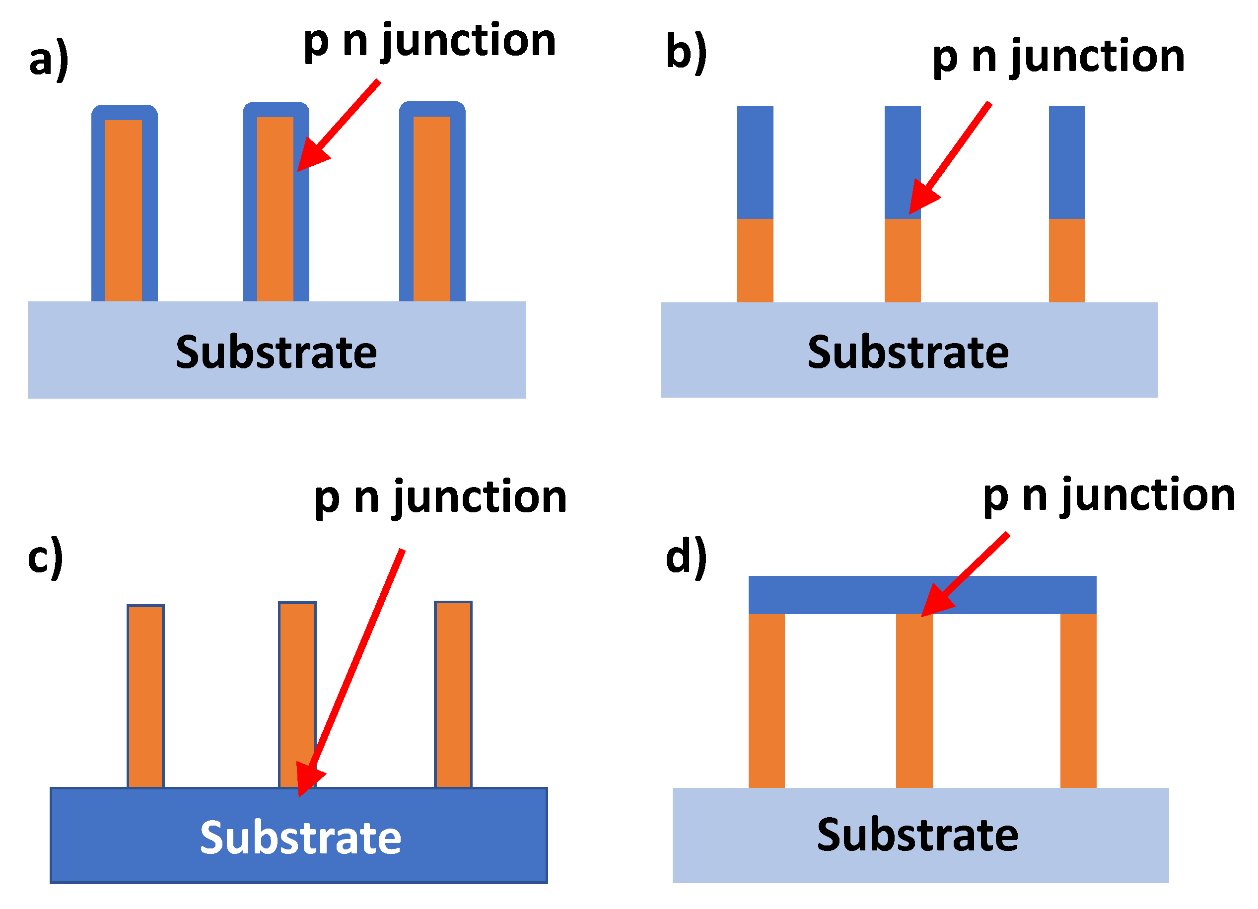
2.1. p-n Junction Design

Nanowire-based solar cells can be classified into four well-defined types: (i) radial p-n junction (is also called core-shell p-n junction) [31,32]; (ii) axial p-n junction [33]; (iii) substrate p-n junction [34]; and (iv) stamped p-n junction [35] as shown in Figure 1. For nanowire-based hybrid solar cell, the design requirements of the other material are that it should be (i) a p-type material; (ii) able to passivate SiNW surfaces; (iii) is highly transparent and (iv) a highly conductive material. As PEDOT:PSS can fulfill all above requirements therefore it can be referred as the best choice for SiNW p-n junction and is reported by many researchers [36,37,38,39,40]. Each of the above p-n junction types as discussed above have some advantages and disadvantages but practically only the radial p-n junction can favor for the PEDOT:PSS–SiNW hybrid solar cell. From Table 1, where the highest performing polymer–SiNW hybrid solar cells are tabulated, it is observed that all these solar cells have PEDOT:PSS as a common polymer for SiNW array. Similarly, for each hybrid solar cell the PEDOT:PSS makes radial p-n junction with SiNW array because such radial p-n junction structure efficiently supports both the light absorption and carrier collection perpendicular to each other [41,42,43,44,45,46,47,48].

2.2. Vertically Aligned or Blended SiNW

There are two ways to incorporate SiNWs inside polymer, either polymer is spin coated over the top of vertically aligned SiNW array [35,36,40] or SiNWs are meshed with polymer as blend and are deposited over the surface of substrate [39]. Generally, it is observed that the vertically aligned SiNWs coated with PEDOT:PSS are the most favorable structure for highly efficient solar cells [51]. Vertically aligned SiNW arrays offer some advantages such as (i) provide a physical interface for the separation of exciton; (ii) improve optical absorption; (iii) ease of radial charge (electron) collection, [52]. Therefore, all high performing hybrid solar cells reported in Table 1 have vertically-aligned radial p-n junction for their photovoltaic response.

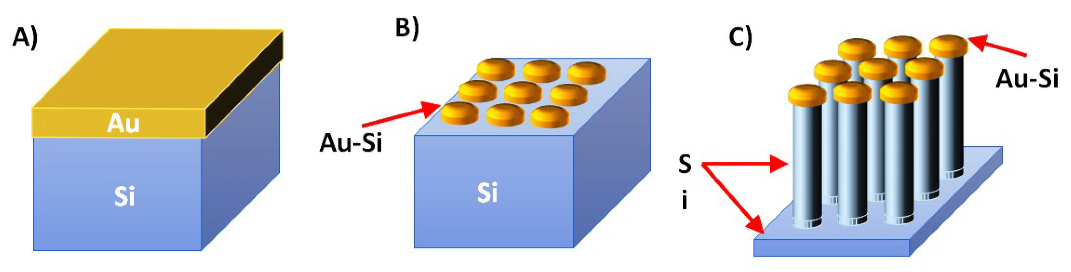
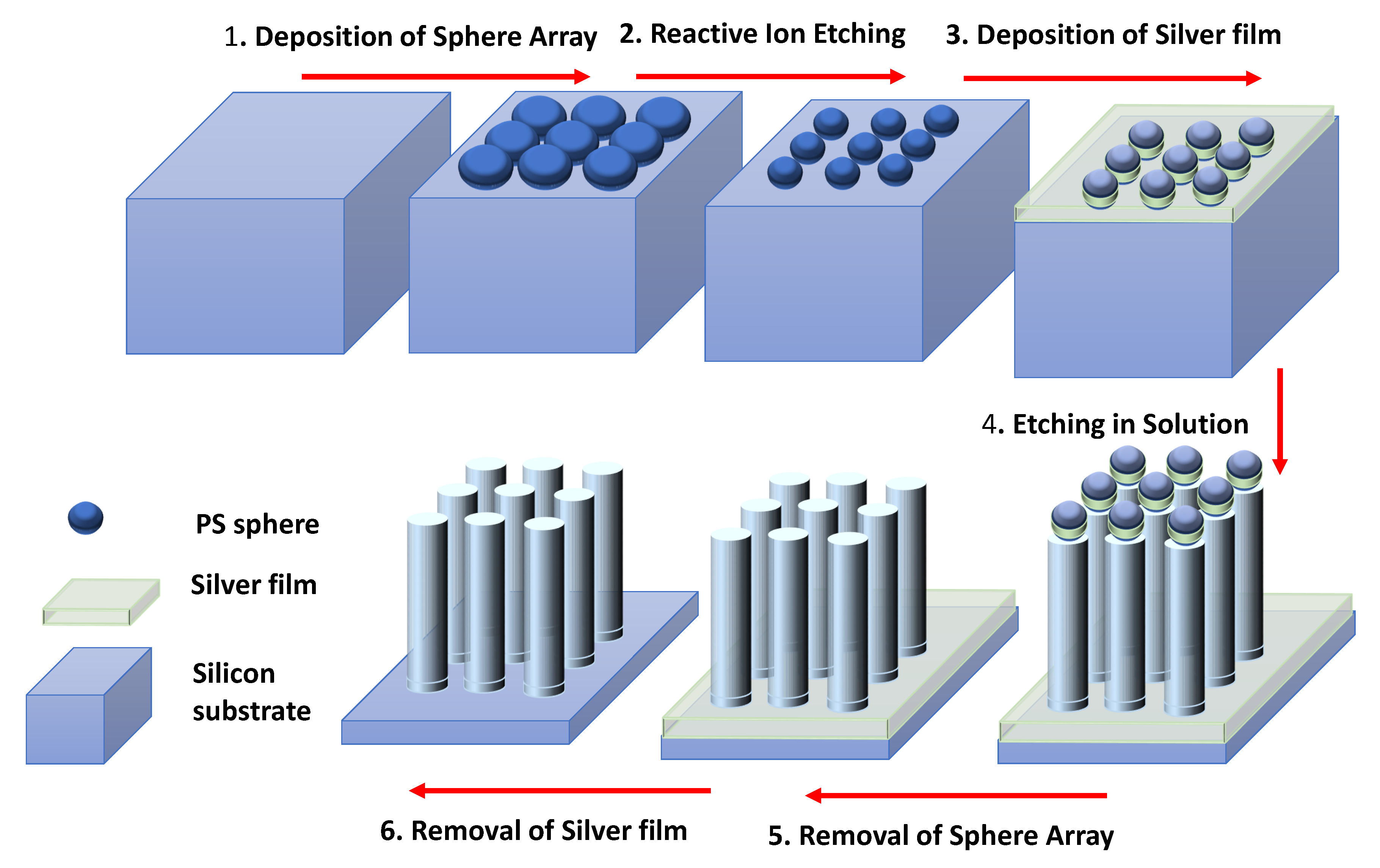
2.3. Fabrication of SiNW

Fabrication of nanowire (similarly SiNW) is not only a science but it is also an art, numerous fabrication techniques have already been reported. Generally, these fabrication methods can be classified with two well-define approaches (i) the bottom-up approach and (ii) the top-down approach [53,54]. Experimentally, it is observed that the bottom-up approach has some freedom of advantages regarding the nano morphology control as compared to the top-down approach. In the bottom-up approach, SiNWs are grown from seeds with additive manners. Vapor Liquid Solid (VLS) combined with chemical vapor deposition (CVD) is considered the best and the most commonly reported technique for the bottom-up approach [55,56,57,58]. Not only CVD, but many other techniques such as molecular beam epitaxy (MBE) [59], laser ablation [60], evaporation of silicon [61] are also used with VLS for the fabrication of SiNW array. Similarly, other techniques for the fabrication of SiNWs are also used under the title of bottom-up approach. These techniques are (i) oxide-assisted growth [62]; (ii) Solution-Liquid-Solid (SLS) [55] and (iii) template directed synthesis techniques [63].
In the VLS approach for SiNW fabrication, metal nanoparticle (e.g., gold nanoparticle) is used to catalyze silane ( S i H 4 ) decomposition. First, the gold nano-particles are deposited over the top of Si substrate, which chemically react with Si surface atoms to form series of Au-Si alloy droplets. The Au-Si droplets continuously adsorb Si during vapor phase operation and lead toward the growth the SiNW array as shown in Figure 2.
For the top-down approach, SiNWs are carved (etched) from their substrate as shown in Figure 3. While lithography [64], direct reactive ion etching (DRIE) [65] and electroless etching (EE) [66,67,68,69] are the most frequently reported techniques for the top-bottom SiNW fabrication approach. Metal assisted chemical etching (MACE) method is comprehensively reported for the development of the SiNW array especially for PEDOT:PSS–SiNW solar cell application. The Table 1 shows that all the best performing hybrid solar cells have SiNWs fabricated by MACE method. Such method has offered many advantages such as (i) low cost; (ii) very simple; (iii) precisely controlled, highly ordered; (iv) vertically aligned SiNW array; (v) versatile and (vi) large area photovoltaic applications [70,71]. Similarly, using of etchant for MACE method makes SiNW surface very rough and porous, which is highly desirable for optical response of SiNW array [70,72]. However, a noticeable variation in design parameters of SiNWs such as diameter, length, doping, surface defects, etc. are observed when SiNW array is fabricated by MACE or CVD for hybrid solar cell [71]. Similarly, some periodic inconsistencies in the diameter of SiNWs as Si whiskers is also observed when SiNWs are grown by VLS method [73]. For top-down approach, mostly n-type bulk single-crystal silicon wafer is used for the fabrication of the PEDOT:PSS–SiNW solar cell.

2.4. Reduction of Surface Trap States

The electrical, optical and photovoltaic response of silicon nanowire based electronic devices depend on the surface trap states of SiNW because of high surface-volume ratio. These surface trap states (are also called imperfection surface states) are just twinning, stacking or dangling bonds created by strain, structural defects, oxidation-induced defects, catalyst situated at grains, metal impurities and are grown during SiNW fabrication process either by VLS or by etching methods [74,75,76]. Furthermore, SiNW has many localized surface states in addition to these structural defect sates. Single crystalline periodic nature of Si creates the energy band structure and the abrupt termination of this band structure at nanowire surfaces causes to generate localized energy surface states and may become the source of free carrier recombinations just as defect states. Similarly, the SiNWs grown from bottom to up approaches are mostly polycrystalline or amorphous in nature and therefore their surfaces are also full of localized surface traps [77].
Surface states, a combination of both defective and localized states, offer many complexities for solar cell applications. Some of these complexities are uniquely associated with nanowires such as (i) these traps are in large quantity; (ii) uniformly distributed; (iii) exist on the depletion region on the surface; (iv) have multiple facets with different crystal orientations; (v) may become unpredictable due to quantum confinement and (vi) have unpredictable surface potential due to high volume-surface ratio.
The recombination losses for PEDOT:PSS–SiNW solar cell depend on the both dark and photo-current recombination losses. Most photo charges are generated inside SiNWs and very few are generated inside PEDOT:PSS polymer. The dark electron-current is blocked and therefore very few dark-current recombination losses are taken place inside bulk PEDOT:PSS region. However, the SiNW surfaces are full of traps and contribute a major role for recombination losses. Most of these surface traps become the source of electron–hole recombination and lower the carrier diffusion length and mobility for nanowire. Therefore, they degrade photovoltaic parameters and hence severely reduce the power-conversion efficiency of PEDOT:PSS–SiNW solar cell [78].
The main issue with surface trap states is that it is very difficult to control during the device fabrication process and the available remedies are only to manage these trap states. Two most common approaches are used to reduce the effects of these surface traps of SiNW such as to passivate the nanowire surfaces and/or shrink the surface area of nanowires (nano-cone, pyramid, tapered-nanowire, etc.) [79,80]. Passivation is commonly performed in which some molecules are tried to attach at the surfaces of SiNWs and many robust materials are reported for passivation such as silicon-nitride ( S i N X ) [81], hydrogenated amorphous-silicon ( a S i : H ) [82] and thin-film of amorphous aluminum-oxide ( a A l 2 O 3 ) [82]. Among these materials, amorphous Si ( S i N X , S i O 2 , etc.) shows the best performance therefore Wang et al. performed two step passivation, in the first step SiNW are treated with O 2 plasma and in the second step SiNWs are passivated with S i O 2 for PEDOT:PSS–SiNW solar cell [83]. Recently organic molecules are also reported for silicon nanowire passivation [84] and even solute PEDOT:PSS is also reported as a passivating material [85]. On the other hand, PEDOT:PSS is not only passivate the surface traps of SiNW but it also copes the stacking as well as twinning defects of SiNWs without requiring any lattice matching for PEDOT:PSS–SiNW solar cell [49]. Generally, the passivating materials are also used to suppress the interface chemical reactions and traps states between PEDOT:PSS and SiNWs to improve the efficiency, reliability and stability of PEDOT:PSS–SiNW solar cell [50].
It is experimentally as well as theoretically observed that the functional groups of passivating material hybridized the surface valence band of SiNW and cause to reduce the energy bandgap especially for low diameter nanowire [86]. The diameter of SiNW can be manipulated by controlling thermal oxidation time during the fabrication process. On the other hand, the work function of PEDOT:PSS can also be tailored by changing the content of PSS [87], hence the optimum band structure of both materials can be tailored for a highly efficient PEDOT:PSS–SiNW solar cell.

2.5. Doping of SiNWs

Doping is one of the most influential parameters for the designing of p-n junction for SiNW-based solar cell [88]. The conventional methods of doping like thermal diffusion as well as ion implantation are not suitable to realize good quality shallow p-n junctions for 3-D SiNWs, because ion implantation method causes serious lattice-defects and thermal-diffusion process fails to create sharp interfaces for p-n junction. For n-type doping for SiNW array, different approaches are used for top-bottom and bottom-up methods. In etching method, n-type silicon wafer as substrate is used with required doping concentration, while for VLS method SiNW are doped by introducing phosphine (PH 3 ) gas as precursor during in-situ process [89]. The incorporation of phosphine during VLS process disturbs the SiNW growth behavior (hence morphology) which in turn causes to change the SiNW surface energy [90]. This change of surface energy is the main cause of faceting, which is detected on the surface of SiNW grown by VLS method and the observed faceting is the direct function of doping concentration [91]. As compared to the intrinsic, the phosphine lowers the growth rate of doped SiNW by 8% and the maximum doping of SiNW can be achieved up to 1.5 × 10 20 cm 3 due to the limitations imposed by the solubility and thermodynamic process during VLS method [89,90,91,92].

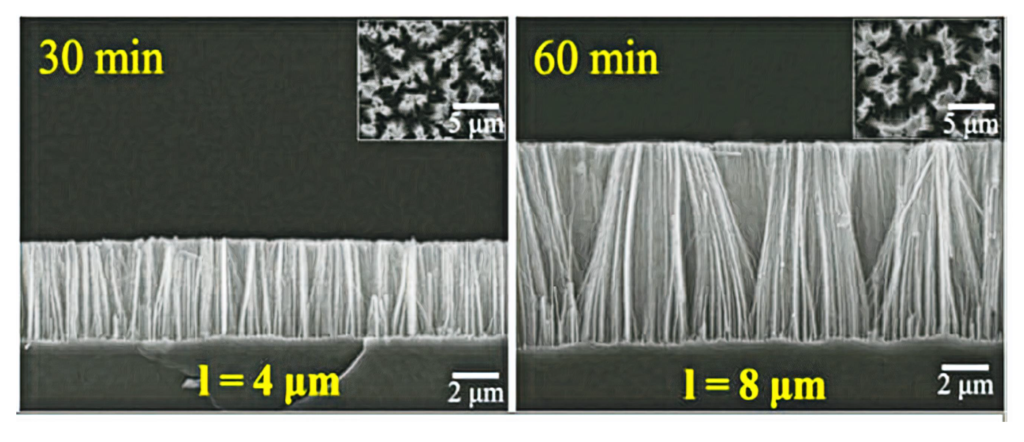
2.6. Removing SiNW Agglomeration

The photovoltaic response of PEDOT:PSS–SiNW solar cell is severely degraded in the presence of agglomerated SiNWs. When PEDOT:PSS is deposited on the top of agglomerated SiNW array, then it covers only bundles of SiNW array and can not penetrate into the bottom of individual SiNW inside the agglomerated SiNW due to the unavailability of physical spaces to reach their bottom. This uncovered space at the bottom of SiNW is occupied by voids and degrade the charge transport process inside PEDOT:PSS [33].
In most of the cases when SiNW length is increased beyond a certain extent then the upper portion of the nanowires tends to combine and form bundles as shown in Figure 4. Formation of bundles depends on the two attractive forces i.e., van der Waals and capillary forces; these forces try to attract the vertically aligned SiNWs arrays [93]. As free-standing SiNW array has very strong mechanical support at their bottom, therefore the top part of SiNW array mechanically bends and tends to agglomerate under the influence of these forces as shown in Figure 4. Zhao et al. have investigated that the size of nanowire cluster depends on the nanowire length, diameter, density, surface tension and many other factors during the fabrication process [94].
The agglomeration of SiNWs is a serious problem for high efficiency PEDOT:PSS–SiNW solar cells and may create some other limiting issues such as (i) PEDOT:PSS does not penetrate into the bottom of SiNWs inside the bundle and hence a void of insulating vacuum or entrapped air is created to deteriorate the charge transport process; (ii) also degrades the electrical and optical properties of SiNW array [95] and (iii) causes to increase the series-resistance and decrease the shunt-resistance of a photovoltaic device [88]. Therefore, it is highly recommended to overcome the agglomeration of SiNW for efficient PEDOT:PSS–SiNW solar cells [96]. In literature, three different approaches are commonly being used to avoid agglomeration
  • By using low surface tension solvent: As agglomeration of SiNW is a direct function of solvent used during etching process, therefore low surface tension solvents instead of water ( surface tension = 75.64 mN/m) are used to avoid agglomeration during the etching process [97]. These solvents are generally ethanol (surface-tension = 22.27 mN/m), methanol (surface-tension = 22.6 mN/m), n-hexane (surface-tension = 18.4 mN/m), n-octane (surface-tension = 21.8 mN/m), etc.
  • Post-treatment after fabrication of SiNWs: In this method agglomerated SiNW are separated either by wet or dry etching treatment. In wet etching technique, Potassium Hydroxide (KOH) or Tetra Methyl Ammonium Hydroxide (TMAH) solution is used to taper the top agglomerated bundle of nanowire. Generally, KOH is the better option as compared to the TMAH [98,99]. In dry etching method, the agglomerated SiNW are separated by passing them through a dry-phase post plasma treatment in an RIE system, but the main drawback of this method is the creation of defects on the surface of SiNW.
  • Togonal method: Togonal et al. has proposed a simple two step process for the fabrication of SiNW by etching method which can improve the top agglomeration of SiNWs. In the first step, the Si substrate is hydropholically pre-treated before the etching process and then the already developed SiNW array is hydrophobically post-treated in the second step. It is well-reported that these steps can lead to the formation of SiNW array with high density and larger nanowire-length with very little agglomeration [100].

2.7. Large Area Application

Commercial point of view, those solar cells which have large-area and fulfill other efficiency requirements can have the potential to replace the wafer-based conventional Si solar cell. For polymer–nanowire hybrid solar cell, both PEDOT:PSS and SiNW inherently support the large area fabrication process. Therefore, for the fabrication of large area PEDOT:PSS hybrid solar cell, the SiNW array is mostly fabricated by metal-assisted electroless etching and then PEDOT:PSS is simply spin coated over the large-area SiNW array. Generally, the solar cell with active area above 1 cm 2 is consider for large area solar applications and many researchers have already fabricated various large-area PEDOT:PSS–SiNW solar cells [95,101,102,103,104]. Kwang-Tae et al. have reported large-area (6 × 6 cm 2 ) PEDOT:PSS–SiNW solar cells with PCE 13.2% but still the long term stability is a serious issue and needs to be solved for further progress [105].

2.8. Stability of Hybrid Solar Cell

It is extensively reported that like other conducting polymers, the PEDOT:PSS also faces some stability issues for PEDOT:PSS–SiNW hybrid solar cells [27,106,107,108]. Therefore, the performance of PEDOT:PSS–SiNW hybrid solar cell degrades as PEDOT:PSS reacts chemically even in the presence of normal humidity and oxygen level. In the acidic environment the oxygen forms O O H + complexes and leads to the following chemical reactions [109]
PEDOT + OOH+ → PEDOT+ + OOH*
PEDOT+ + OOH* + H+ → PEDOT2+ + H2O2
Such chemical reactions aggressively degrade the photovoltaic response at high degree of self-heating and the main sources of self-heat generation are non-radiative recombination, light absorption and joule heating inside the hybrid solar cell [110]. As discussed above, most of the passivating materials can also suppress the oxidative chemical reactions between PEDOT:PSS and SiNWs in addition to lower the recombination losses in order to enhance the reliability and stability of the PEDOT:PSS–SiNW solar cell [111]. Yu et al. used 1,1-bis[(di-4-tolylamino)phenyl]cyclohexane (TAPC) layer as intermediate passivating material between SiNW and PEDOT:PSS for a 13.1% efficient solar cell and it is observed that TAPC suppress the oxidation chemical reaction as well as interface traps for an efficient and stable hybrid solar cell [50].

3. Electrical Design of SiNW for Hybrid Solar Cell

The current (I)-voltage (V) characteristics of a solar cell under the influence of applied electric field is considered as a dark-current or simple electrical response of a solar cell. The PEDOT:PSS–SiNW solar cell behaves like a metal-semiconductor Schottky diode and can be modeled with one-diode equivalent circuit. Where, the diode parameters such as series resistance R S , shunt resistance R S H and diode ideality-factor (n) are co-related as to define their electrical response [112,113,114].
I = I L I o e x p V + I R S n V T V + I R S R S H
where V T = k T q is the thermal voltage, T is ambient temperature, k is Boltzmann constant, I o is saturation current and I L is photo-current. Just like optical, the designing of electrical response of PEDOT:PSS–SiNW solar cell is also very important to realize highly efficient hybrid solar cells and it depends on both the electrical properties of PEDOR:PSS as well as SiNW array. For efficient SiNW electrical response, the two issues that must be addressed are the minority carriers’ diffusion-length should be long enough and the recombinational losses should be minimum. For bulk silicon, the minority carrier lifetime is not so bad as compared to PEDOT:PSS (>10 ns), but for SiNWs it is a direct function of nanowire’s diameter, the higher diameter means higher the minority carrier’s diffusion length. Similarly, the optical absorption is also improved with increasing the diameter as well as the length of SiNWs [115]. On the other hand, the major sources of recombination losses are the density of surface traps, which are distributed throughout the nanowire surfaces. When diameter and length of SiNW is increased then the surface-volume ratio is also increased and hence surface traps are also multiplied. Therefore, optimum nanowire diameter and length is needed for efficient PEDPT:PSS–SiNW solar cells [116,117].
Despite the removal of SiNWs agglomeration at the top, the PEDOT:PSS still fails to penetrate completely into the bottom of SiNWs which reduces the contact area between PEDOT:PSS and SiNWs and as a result voids are formed. Electrical and hence photovoltaic parameters are affected by these voids. Lu et al. proposed a simple but efficient idea by filling SiNW array with ethanol for proper coverage of PEDOT:PSS especially at the bottom of SiNWs [40].

3.1. Diode-Ideality Factor

Among other parameters, the diode ideality factor ( n ) is used to define the degree of quality between PEDOT:PSS–SiNW interfaces in term of surface traps [23,114,117,118]. Higher surface traps between PEDOT:PSS–SiNW interfaces leads to the higher recombination losses and hence higher will be the diode ideality-factor ( n 1 ) , while n = 1 is used for an ideal diode (means no traps and no recombination losses). It is observed that the diode ideality factor can be improved by passivating the surface of SiNWs [119].

3.2. Shunt Resistance

Shunt resistance ( R S H ) is the symbolical representation of the leakage current resistance, large value of shunt resistance imply strong resistance to the undesirable leakage current in the PEDDOT:PSS–SiNW solar cell. The shunt resistance of a solar cell can be calculated from the slope at J S H point on their photo current–voltage response as
d I d V J S H = 1 R S H
Small value of the shunt resistance causes to lower the fill-factor and open-circuit voltage and then power-conversion efficiency of a solar cell. Therefore, it is necessary to increase the shunt resistance for an efficient PEDDOT:PSS–SiNW solar cell. Generally, the low value of shunt resistance or large shunt-leakage current occurs in PEDDOT:PSS–SiNW solar cells due to high density of a surface traps and impurities between PEDDOT:PSS and SiNW interfaces, which can be improved by applying passivation on SiNW surfaces [83,120]. As higher nanowire length or diameter cause to enhance the surface trap density and impurities therefore very low shunt resistance is reported for such hybrid solar cell [120].

3.3. Series Resistance

The high series resistance ( R s ) in PEDDOT:PSS–SiNW solar cells also causes to lower the fill-factor and short-circuit current and hence power-conversion efficiency of a solar cell and the value of R S H can be estimated from the slope at V O C point on their photovoltaic response.
d I d V V O C = 1 R S
The series resistance in a PEDDOT:PSS–SiNW solar cell is the combination of three resistances, (i) resistance of bulk region of both SiNW and PEDOT:PSS region; (ii) the contact-resistance between SiNW and silicon substrate and the contact-resistance between PEDOT:PSS and anode metal; and finally (iii) the resistance of the cathode and anode metal contacts itself. As conducting polymers are inherently high resistivity materials compared to single-crystal doped silicon [121,122], therefore the n-SiNW role is negligible and R S is dominantly contributed by either bulk or contact resistance of PEDOT:PSS for the PEDDOT:PSS–SiNW solar cell. The contact resistance and the conductivity can be improved by many methods as reported in [123,124].

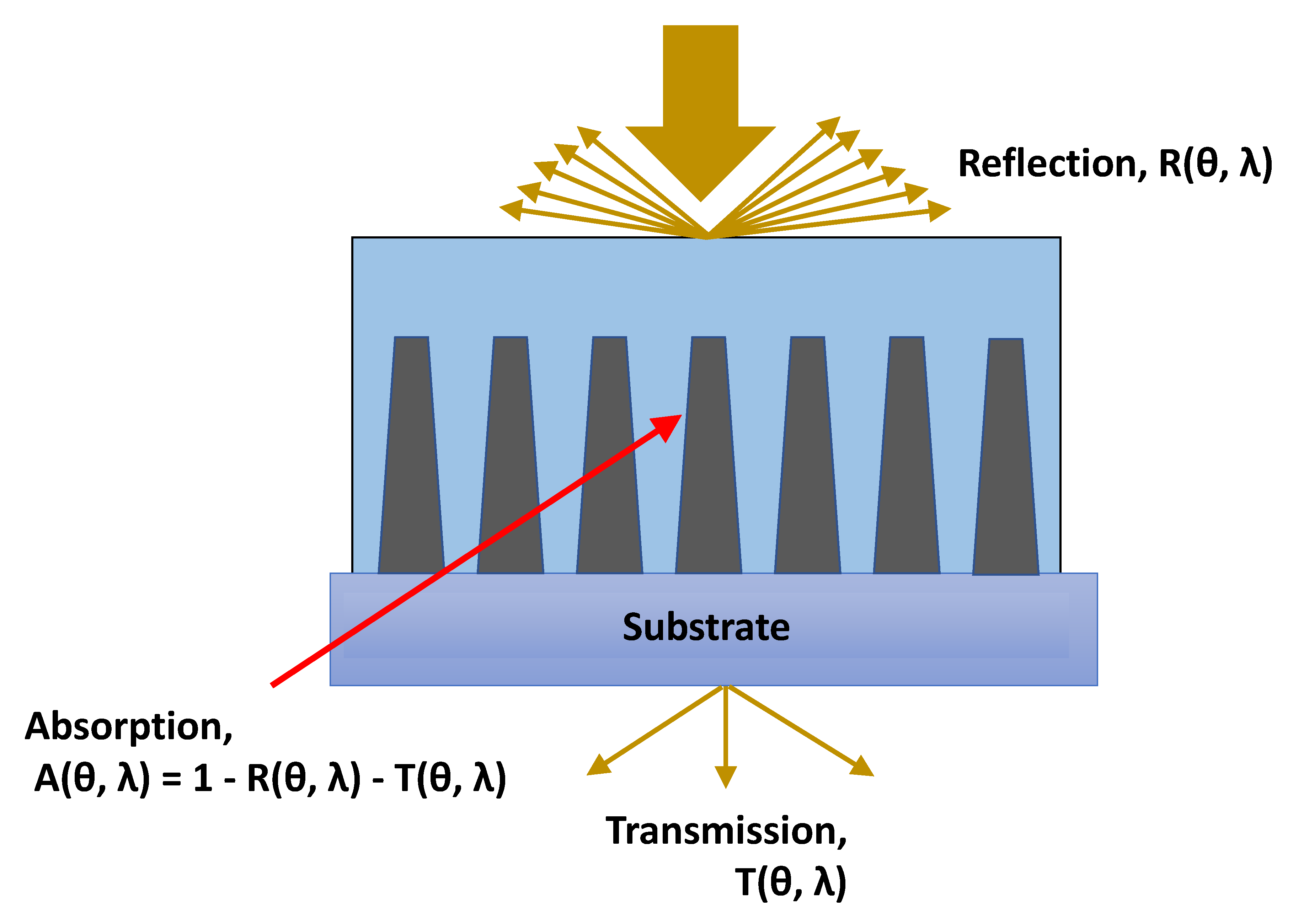
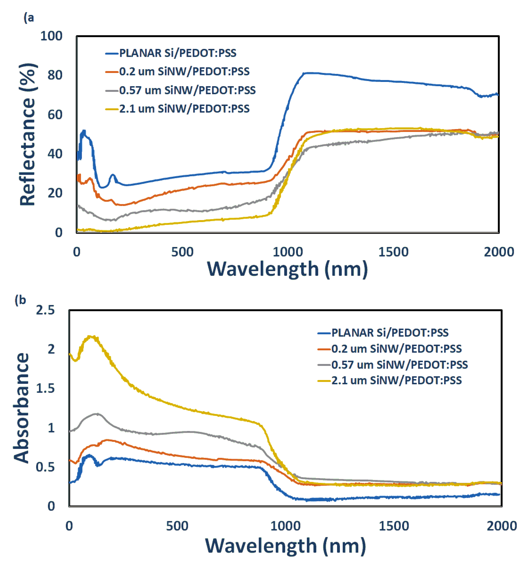
4. Optical Response of SiNW for PEDOT:PSS–SiNW Solar Cell

Compared to electrical, the optical properties are a strong function of the SiNW’s length (L), diameter (D) and periodicity (P) for the PEDOT:PSS–SiNW hybrid solar cell. The SiNW structure offers unique optical properties of direct and tuneability of energy bandgap either by reducing the diameter or by using the passivation of nanowire. These properties make SiNWs as an ideal choice for high efficiency PEDOT:PSS–SiNW solar cell [81]. The PEDOT:PSS behaves like a transparent electrode and provides an optical window to SiNW array for photovoltaic response. The optical parameters of PEDOT:PSS–SiNW such as reflection (R), absorption (A) and transmission (T) are not only a function of incidence angle ( θ ) but are also the wavelength function of the incident light as shown in Figure 5. For most of the practical cases the transmission losses for the PEDOT:PSS–SiNW solar cell are negligible due to thick substrate and as well as back substrate electrode. Therefore, these optical parameters can be determined as
A θ , λ = 1 R θ , λ T θ , λ
Absorption of photons inside the SiNW array is a stochastic process and the probability of the photon absorption rises sharply with the enhancement of optical diffusion length. Enhancement of optical diffusion length depends on the multiple reflection of photons inside SiNWs for PEDOT:PSS–SiNW hybrid solar cell. Therefore, the optical absorption performance can be explored with the help of optical reflectance measurements.
The SiNWs show excellent antireflection response for the PEDOT:PSS–SiNW solar cell. However, a strong antireflection response cannot provide a guarantee for higher optical absorption because the fruitful absorption of the cell is hindered by the parasitic absorption by substrates, electrode–substrate interfaces and defects of nanowire surfaces. On the other hand, the PEDOT:PSS–SiNW junctions play some beneficial role for further optical absorption due to the smooth change in the refractive index between air, PEDOT:PSS and SiNWs array [125].
When light falls on a PEDOT:PSS–SiNW solar cell as shown in Figure 5, the optical interferences play some role to define specific diffraction-patterns. These diffraction-patterns influence the wavelength dependent optical response especially light trapping of PEDOT:PSS–SiNW solar cell [126]. Under the influence of these patterns the optical path is increased due to the multiple scattering inside SiNW array (light trapping) before either absorption or transmission outside the array. The quality of light trapping depends on the incident wavelength ( λ ) and the dimension of SiNWs (as PEDOT:PSS offers optical window for SiNW array) yields to the three possible cases. These cases are: (i) when periodicity of nanowire is higher than the incident wavelength ( P λ ) then the shorter wavelength (high energy photons) offers higher optical losses because of higher reflection and transmission; (ii) when λ is very close to the dimension of SiNWs ( λ P ) , then the light trapping is improved with little transmission and finally (iii) when incident wavelength is larger than the periodicity of nanowire ( λ P ) than the longer wavelength (low energy photons) faces few scattering before absorption. Figure 6 clearly demonstrates the three well-define regions for both absorption as well as reflection of the PEDOT:PSS–SiNW solar cell.
The graded refractive index (GRI) based on SiNW array strongly suppresses the optical reflection as compared to the conventional silicon thin film [98,127,128]. The tapered, nano-cones, pyramid, etc. based SiNW array with PEDOT:PSS for hybrid solar cell offers a unique architecture of GRI to supress the optical reflection and hence improve the absorption, many researchers have already reported such architecture for an efficient PEDOT:PSS–SiNW solar cell [128,129]. The light trapping of the SiNWs is directly affected by the degree of randomness in the diameter and as well as the spacing between nanowires. Generally the SiNW array which has various distributions of diameter, spacing and growth direction demonstrates a very strong light absorption compared to highly ordered SiNWs for solar cell [130,131]. The fabrication of random SiNWs is a relatively a simple task, by paying no special attention to make them ordered as SiNW fabrication naturally involves many random processes [132,133,134]. The improved optical and photovoltaic response is also observed for many efficient PEDOT:PSS–SiNW solar cells where disordered SiNW arrays are used.
Not only geometry but also the orientation of SiNWs either as inclined (tilted, slanted) or vertically aligned plays a role for improved light trapping and therefore strong optical absorption is observed for inclined SiNW array [135,136,137,138,139]. Hong et al. performed comprehensive simulation and modeling and discovered that the uppermost optical absorption efficiency of slanted SiNW (P = 800 nm and D / P = 0.7) is 33.45%, compared to vertically aligned SiNW (which is close to 28.36%) [140]. Such optical absorption improvements for slanted SiNWs can be attributed by the excitation of other additional optical resonant modes [136]. Despite higher efficiency, slanted SiNW array is highly unsuitable geometry for PEDOT:PSS–SiNW solar cells due to many reasons: (i) lack of deep penetration of PEDOT:PSS towards the bottom of SiNWs, (ii) well-designed and vertically aligned SiNWs can sufficiently offer good optical absorption and (iii) the most important reason is that the fabrication of slanted SINW with specific angle is sometime difficult task and very limited fabrication options are available. Therefore, negligible slanted SiNW arrays for PEDOT:PSS–SiNW solar cells are reported.
Optical reflection as well as absorption is also the function of nanowire length for PEDOT:PSS–SiNW solar cells as shown in Figure 6 [93]. The figure clearly demonstrates that both reflection and absorption spectra are significantly improved for PEDOT:PSS–SiNW solar cells compared to planar PEDOT:PSS–SiNW due to many reasons as discussed above. Similarly, it is also observed the highest SiNW length solar cell shows the best suppression and hence absorption of light between 250 to 1000 nm wavelength. On the one side, the optical absorption is improved at higher lengths of SiNWs, while on the other side the higher length also offers higher surface traps to degrade the electrical and photovoltaic response, therefore optimization of SiNW’s length is required for an efficient PEDOT:PSS–SiNW solar cell.

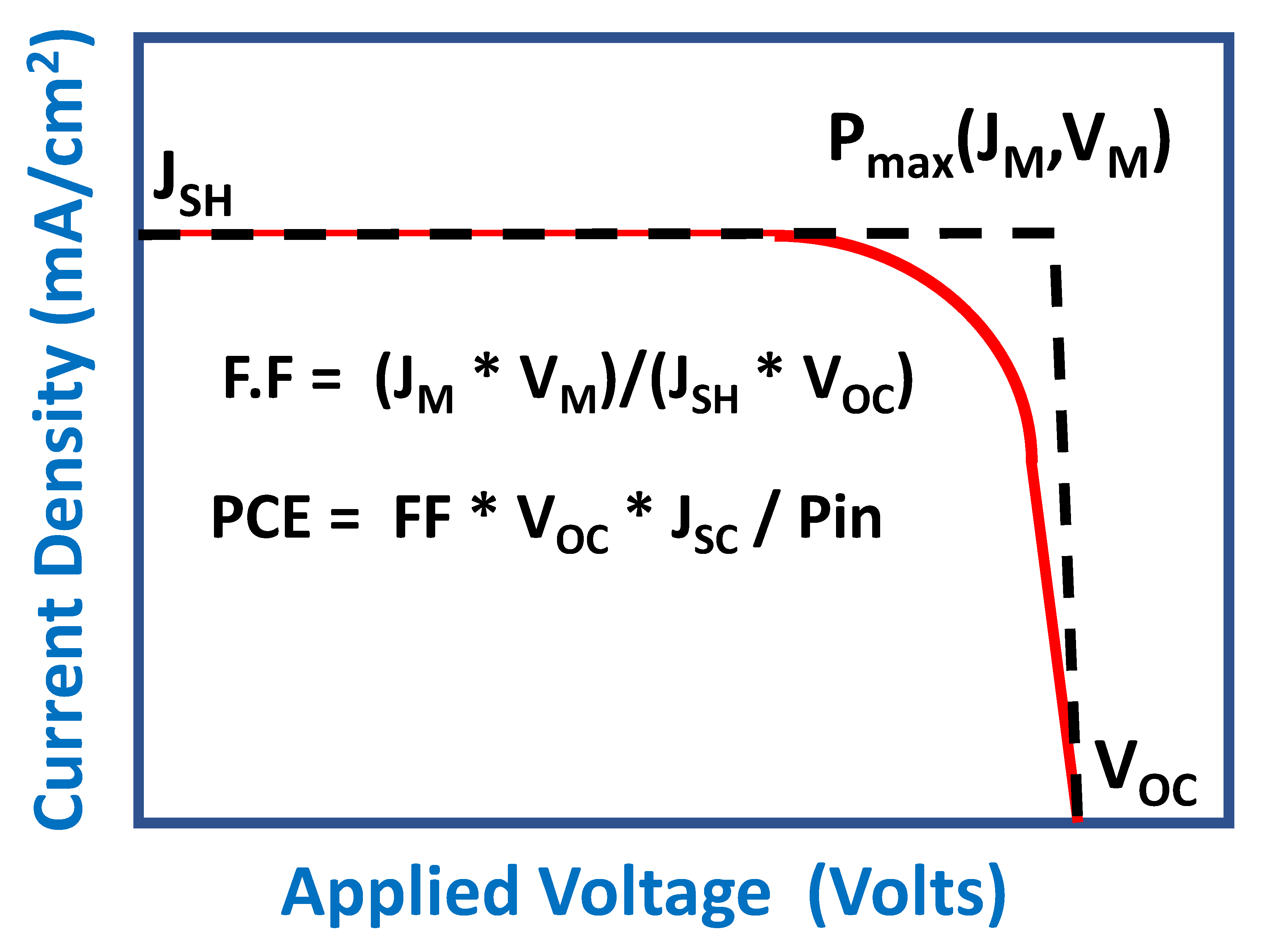
5. Photovoltaic Design of SiNW

When light falls on a p-n junction, electron–hole pairs are generated and are traveled to their respective electrodes under the influence of internal potential and give rise some electricity, this process is referred as photovoltaic response of given p-n junction as shown in Figure 7 [141]. Similar to other solar cells, the photovoltaic response of PEDOT:PSS–SiNW hybrid solar cell consists of five main steps: (i) absorption of photons; (ii) generation of electron–hole pairs; (iii) dissociation of excitons; (iv) transportation of free carriers and v) collection of free carriers at respective electrodes [142]. The power-conversion efficiency (PCE) of a solar cell depends on all of these steps and can be summarized in three parameters: short-circuit current J S C , open-circuit voltage V O C and fill-factor (FF). The PCE of a solar cell can be defined as the ratio between maximum power delivered to the input power P I N as shown in Figure 7.

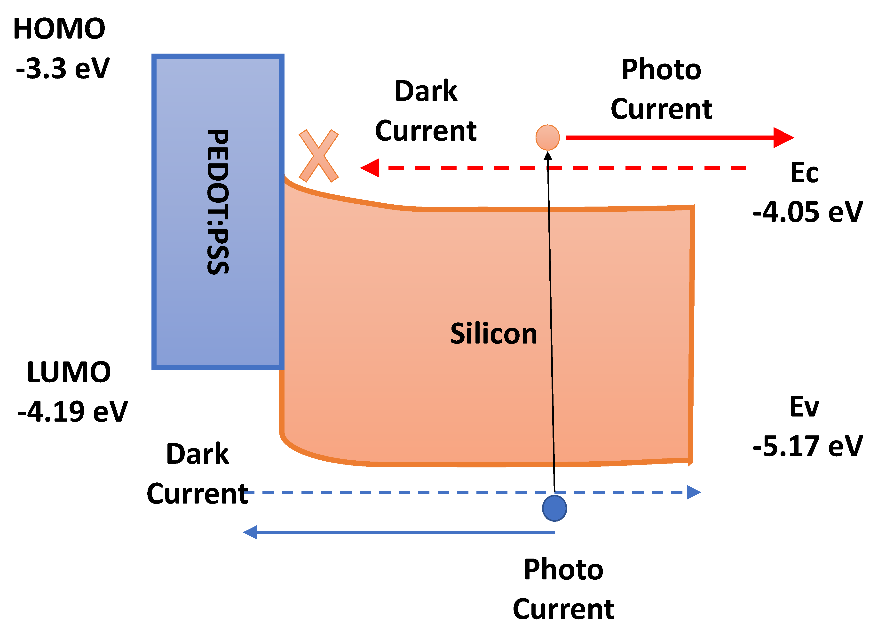
5.1. Photovoltaic Mechanism of PEDOT:PSS–SiNW Hybrid Solar Cells

The energy-band diagram of a PEDOT:PSS–SiNW hybrid solar cell is a very useful tool to understand the mechanism of charge separation and carrier transport process as shown in Figure 8. The PEDOT:PSS is a conducting polymer that has a work function of 4.9 eV (Eg 1.6 eV, Highest Occupied Molecular Orbital (HOMO) 3.3 eV, Lowest Unoccupied Molecular Orbital (LUMO) 4.19 eV) and heavily doped PEDOT:PSS–SiNW is used for the hybrid solar cell [106]. Just for qualitative discussion, the bulk energy bandgap of silicon is used here because SiNW energy bandgap is little different from bulk Si energy bandgap. Generally, SiNW energy bandgap depends on the nanowire diameter and its crystallographic direction [75,143]. When PEDOT:PSS–SiNW solar cell is illuminated, most of the photons are absorbed by SiNW, as PEDOT:PSS is a transparent material and SiNWs show excellent optical absorption. This is mainly due to multiple reflection by nanowires inside array which enhanced optical length for absorption [144,145]. Generally, heavily doped PEDOT:PSS is used and a depletion region is formed inside n-type SiNWs and hence optical absorption in this depletion region cause to generate large number of photo electron–hole pairs. The PEDOT:PSS–SiNW depletion region splits the photogenerated electron and holes and causes a photo-current. Consequently, two but opposite direction photo current ( I L ) and dark current ( I D ) flow inside the hybrid cell. Due to the E C level mismatch between Si and PEDOT, the I D is blocked by PEDOT:PSS and reflected back to the cathode. The blocking of the I D is significantly improved by using external layer of passivation across SiNWs [29]. On the other hand, the dark hole current flows through PEDOT:PSS toward anode as a result of the valence-band matching of both polymer and nanowire. The overall flow of currents leads to the short-circuit current and open-circuit voltage as shown in Figure 8 [146].

5.2. Effects of SiNW’s Surface Traps

The recombination losses for PEDOT:PSS–SiNW solar cells depend on minority carriers diffusion length. The effective carrier diffusion length L e f f is directly proportional to the carrier life time τ e f f as [147]
L e f f = D τ e f f
where, D is the diffusion coefficient of carriers inside SiNW. If ϕ and τ b are the SiNW diameter and Si bulk carrier life time then the effective carrier life time τ e f f can be co-related to the surface recombination velocity S as
1 τ e f f = 1 τ b + 4 S ϕ
Above equation clearly demonstrates that the lower value of the minority carrier life time gives higher recombination velocity and hence higher losses. When light falls on the PEDOT:PSS–SiNW solar cell then a large number of photo charges are generated inside SiNWs compared to PEDOT:PSS polymer. As shown in Figure 8, the dark electron-current is blocked and therefore very few dark-current recombination losses are taken place inside bulk PEDOT:PSS region. However, the SiNW surfaces are full of traps and high surface-volume ratio cause to increase the surface recombination velocity and hence losses. Most of these surface traps become the source of electron–hole recombination and lower the carrier diffusion length and mobility for nanowire as stated by above equations. At the same time, all these parameters also degrade the photovoltaic response and hence severely reduce the power-conversion efficiency of the PEDOT:PSS–SiNW solar cell [148].

5.3. Improvement in PV Response

As discussed above, the photovoltaic response of PEDOT:PSS–SiNW solar cell depends on J S C , V O C and FF. The J S C of PEDOT:PSS–SiNW solar cell is a function of the optical absorption, charge separation at PEDOT:PSS and SiNW interfaces and charge collection at respective electrode. Charge collection from SiNW to cathode and from PEDOT:PSS to anode can be optimized by applying different electrode engineering methods [49]. The main reasons for poor photovoltaic performance of PEDOT:PSS–SiNW solar cell is the SiNW surface recombination losses due to inefficient SiNW surface passivation, excessive agglomeration of SiNWs, lack of proper PEDOT:PSS coverage across SiNWs and inadequate design of solar cell.

5.4. Improvement in J S C

The PEDOT:PSS is a conducting p-type polymer, it has very low mobility as charges are hopped from one molecular-chain to other molecular-chain similar to other conducting polymers [149,150]. The PEDOT:PSS can passivate but still proper passivation is required for SiNW surfaces. PEDOT:PSS provides an electric path to free carriers after exciton separation at PEDOT:PSS–SiNW interfaces for higher short-circuit current. Similarly, if the coverage of PEDOT:PSS is not proper along SiNW surfaces (specially at bottom side) then it has very high probability of recombination losses, which severely degrade the short-circuit current [151].
In order to improve the coverage of PEDOT:PSS along SiNWs, different solutions have been reported such as removing the agglomeration of SiNWs [127], tuning the density of SiNWs [78], using nanocones SiNWs [152], using tapered SiNWs [80], using micro-pyramid silicon wire [153], fabrication of SiNWs by template method [128] and so on. Despite of these techniques, the efficient coverage of PEDOT:PSS along SiNW is still a challenging task due to the (i) agglomeration of the long nanowires; (ii) polymeric nature of PEDOT:PSS (large molecular chain) and (iii) fast drying process of PEDOT:PSS [154] and therefore, comprehensive research is required.

5.5. Improvement in V O C

The photovoltaic parameters such as short-circuit, open-circuit voltage and fill-factor are inter-related to each other and therefore in literature various techniques which are used to improve the short-circuit current can also use to improve the open-circuit voltage at the same time for solar cell [155,156,157]. From equivalent circuit (see Equation (1)), the V O C is equal to the voltage across R S H subtracted by the voltage drop across R S and higher the R S H give higher V O C (Ohms law). Where R S H is directly related to the leakage current resistance, so reducing the leakage current ( J O ) will give higher V O C as evident from the bellow equation,
V O C = k T q J S C J O + 1
where q is charge, k is Boltzmann constant and T is ambient temperature. The recombination losses at SiNW surface traps are the main source of leakage current and SiNW passivation is the best and simple way to improve V O C as well as J S C for the PEDOT:PSS–SiNW solar cell. Therefore, it can be inferred that improvement in J S C also improves the V O C as evident from Equation (7). Yu et al. used 1,1-bis[(di-4- tolylamino)phenyl]cyclohexane (TAPC) to passivate SiNW surface for PEDOT:PSS–SiNW solar cells to enhanced V O C and FF leads to PCE up to 13 % [50]. Generally, the passivation of SiNW surface is used to improve the open-circuit voltage, fill-factor as well as short-circuit current. According to a rough estimation, the FF and V O C can be further enhanced up to 15–20% by suppressing the surface trap states by the order 2 in magnitude, which is not a difficult task by using conventional semiconductor processing technologies. Zhang at. al. passivated the silicon pyramid by hydrogenated-amorphous silicon for the PEDOT:PSS–Si hybrid solar cell for the enhancement of open-circuit voltage from 548 mV to 620 mV and as a result the PCE is improved from 8.3% to 12%, respectively. He further improved the open-circuit voltage toward 634 mV with PCE 16.1% by using inverted structure and proved that the proper optical utilization through inverted structure can also be used to improve the open-circuit voltage [158]. Similarly, Jiang et al. reported that low filling (larger periodicity) of SiNWs with PEDOT:PSS create a strong inversion layer close to the SiNW surfaces and this inversion layer reduces the surface recombination losses and hence improved open-circuit voltage and FF leads to efficiency up to 13.11 % [51].

6. Conclusions

In this review, we primarily concentrate on the general, electrical, optical and photovoltaic design issues of the SiNW array for efficient PEDOT:PSS–SiNW hybrid solar cells. The photovoltaic response of PEDOT:PSS–SiNW is very complex in nature and many design issues of the SiNW array are required to optimize the solar cell for higher efficiency. The radial p-n junction with vertically aligned SiNW is the most favorable structure as it offers optical absorption and carrier collection separately to each other for PEDOT:PSS–SiNW hybrid solar cells. The randomness of SiNWs also plays a vital role along with its geometry and direction, which improves light trapping and strong optical absorption for the PEDOT:PSS–SiNW hybrid solar cell. The photovoltaic response of a hybrid solar cell is degraded in the presence of SiNW’s surface trap states, which are the major sources of leakage current for recombination losses. These traps states can be reduced either by using the various passivation techniques or by reducing the surface to volume ratio by tapering the SiNWs. Although PEDOT:PSS can passivate, a separate passivation for SiNW surfaces is required before PEDO:PSS deposition over SiNW array. The passivation of SiNW not only improve the short-circuit current, fill-factor but also enhance the open-circuit voltage and hence power-conversion efficiency of the PEDOT:PSS–SiNW solar cell. The proper passivation blocks the oxidative chemical reaction between PEDOT:PSS and SiNW and causes to improve the stability of the hybrid solar cell. The coverage of PEDOT:PSS along a SiNW is very serious concern and severally degrade the photovoltaic response, which can be improved by removing the top agglomeration of SiNW by using the alkali treatment of SiNWs for hybrid solar cell. We believe that this review will help our researchers, experimenters and especially freshers to design and fabricate the high efficiency PEDOT:PSS–SiNW hybrid solar cell.

Author Contributions

The manuscript was written through the contributions of all authors. All authors have read and agreed to the published version of the manuscript.

Funding

The authors would like to thank the Deanship of Scientific Research at Umm Al-Qura University for supporting this work by Grant Code: 18-ENG-1-01-0005.

Acknowledgments

We all are very grateful to Khasan S Karimov for his useful discussion and encouragement.

Conflicts of Interest

The authors declare no conflict of interest.

References

  1. Shafiee, S.; Topal, E. When will fossil fuel reserves be diminished? Energy Policy 2009, 37, 181–189. [Google Scholar] [CrossRef]
  2. Klinenberg, E.; Araos, M.; Koslov, L. Sociology and the Climate Crisis. Annu. Rev. Sociol. 2020, 46. [Google Scholar] [CrossRef] [Green Version]
  3. Sun, X.; Li, Z.; Wang, X.; Li, C. Technology development of electric vehicles: A review. Energies 2020, 13, 90. [Google Scholar] [CrossRef] [Green Version]
  4. Harrington, R. This Incredible Fact Should Get You Psyched About Solar Power. Bus. Insid. 2015. Available online: http://www.businessinsider.com/solar-power-potential-how-much-energy-does-sun-have-2017-3 (accessed on 23 July 2020).
  5. Lee, T.D.; Ebong, A.U. A review of thin film solar cell technologies and challenges. Renew. Sustain. Energy Rev. 2017, 70, 1286–1297. [Google Scholar] [CrossRef]
  6. Alivisatos, A.P. Semiconductor clusters, nanocrystals, and quantum dots. Science 1996, 271, 933–937. [Google Scholar] [CrossRef] [Green Version]
  7. Law, M.; Goldberger, J.; Yang, P. Semiconductor nanowires and nanotubes. Annu. Rev. Mater. Res. 2004, 34, 83–122. [Google Scholar] [CrossRef] [Green Version]
  8. Garnett, E.; Yang, P. Light trapping in silicon nanowire solar cells. Nano Lett. 2010, 10, 1082–1087. [Google Scholar] [CrossRef]
  9. Wang, J.; Polizzi, E.; Lundstrom, M. A three-dimensional quantum simulation of silicon nanowire transistors with the effective-mass approximation. J. Appl. Phys. 2004, 96, 2192–2203. [Google Scholar] [CrossRef] [Green Version]
  10. Paska, Y.; Haick, H. Interactive effect of hysteresis and surface chemistry on gated silicon nanowire gas sensors. ACS Appl. Mater. Interfaces 2012, 4, 2604–2617. [Google Scholar] [CrossRef]
  11. Zhang, A.; Kim, H.; Cheng, J.; Lo, Y.H. Ultrahigh responsivity visible and infrared detection using silicon nanowire phototransistors. Nano Lett. 2010, 10, 2117–2120. [Google Scholar] [CrossRef]
  12. Zhang, G.J.; Ning, Y. Silicon nanowire biosensor and its applications in disease diagnostics: A review. Anal. Chim. Acta 2012, 749, 1–15. [Google Scholar] [CrossRef] [PubMed]
  13. Li, Q.; Koo, S.M.; Edelstein, M.D.; Suehle, J.S.; Richter, C.A. Silicon nanowire electromechanical switches for logic device application. Nanotechnology 2007, 18, 315202. [Google Scholar] [CrossRef]
  14. Karki, K.; Epstein, E.; Cho, J.H.; Jia, Z.; Li, T.; Picraux, S.T.; Wang, C.; Cumings, J. Lithium-assisted electrochemical welding in silicon nanowire battery electrodes. Nano Lett. 2012, 12, 1392–1397. [Google Scholar] [CrossRef] [PubMed]
  15. Yang, X.; Zhong, H.; Zhu, Y.; Jiang, H.; Shen, J.; Huang, J.; Li, C. Highly efficient reusable catalyst based on silicon nanowire arrays decorated with copper nanoparticles. J. Mater. Chem. 2014, 2, 9040–9047. [Google Scholar] [CrossRef]
  16. Dong, G.; Liu, F.; Liu, J.; Zhang, H.; Zhu, M. Realization of radial pn junction silicon nanowire solar cell based on low-temperature and shallow phosphorus doping. Nanoscale Res. Lett. 2013, 8, 544. [Google Scholar] [CrossRef] [Green Version]
  17. Garnett, E.C.; Yang, P. Silicon nanowire radial p- n junction solar cells. J. Am. Chem. Soc. 2008, 130, 9224–9225. [Google Scholar] [CrossRef]
  18. Grancini, G.; Maiuri, M.; Fazzi, D.; Petrozza, A.; Egelhaaf, H.J.; Brida, D.; Cerullo, G.; Lanzani, G. Hot exciton dissociation in polymer solar cells. Nat. Mater. 2013, 12, 29–33. [Google Scholar] [CrossRef]
  19. Stübinger, T.; Brütting, W. Exciton diffusion and optical interference in organic donor–acceptor photovoltaic cells. J. Appl. Phys. 2001, 90, 3632–3641. [Google Scholar] [CrossRef]
  20. Yaffe, O.; Chernikov, A.; Norman, Z.M.; Zhong, Y.; Velauthapillai, A.; van der Zande, A.; Owen, J.S.; Heinz, T.F. Excitons in ultrathin organic-inorganic perovskite crystals. Phys. Rev. 2015, 92, 045414. [Google Scholar] [CrossRef] [Green Version]
  21. Wu, B.; Wu, X.; Guan, C.; Tai, K.F.; Yeow, E.K.L.; Fan, H.J.; Mathews, N.; Sum, T.C. Uncovering loss mechanisms in silver nanoparticle-blended plasmonic organic solar cells. Nat. Commun. 2013, 4, 1–7. [Google Scholar] [CrossRef] [Green Version]
  22. Lee, J.M.; Kwon, B.H.; Park, H.I.; Kim, H.; Kim, M.G.; Park, J.S.; Kim, E.S.; Yoo, S.; Jeon, D.Y.; Kim, S.O. Exciton Dissociation and Charge-Transport Enhancement in Organic Solar Cells with Quantum-Dot/N-doped CNT Hybrid Nanomaterials. Adv. Mater. 2013, 25, 2011–2017. [Google Scholar] [CrossRef] [PubMed]
  23. Liu, J.; Wang, S.; Bian, Z.; Shan, M.; Huang, C. Organic/inorganic hybrid solar cells with vertically oriented ZnO nanowires. Appl. Phys. Lett. 2009, 94, 173107. [Google Scholar] [CrossRef]
  24. Novotny, C.J.; Yu, E.T.; Yu, P.K. InP nanowire/polymer hybrid photodiode. Nano Lett. 2008, 8, 775–779. [Google Scholar] [CrossRef] [PubMed]
  25. Chang, C.Y.; Tsao, F.C.; Pan, C.J.; Chi, G.C.; Wang, H.T.; Chen, J.J.; Ren, F.; Norton, D.; Pearton, S.; Chen, K.H.; et al. Electroluminescence from ZnO nanowire/polymer composite p-n junction. Appl. Phys. Lett. 2006, 88, 173503. [Google Scholar] [CrossRef]
  26. Bach-Toledo, L.; Hryniewicz, B.M.; Marchesi, L.F.; Dall’Antonia, L.H.; Vidotti, M.; Wolfart, F. Conducting polymers and composites nanowires for energy devices: A brief review. Mater. Sci. Energy Technol. 2020, 3, 78–90. [Google Scholar] [CrossRef]
  27. Hu, L.; Song, J.; Yin, X.; Su, Z.; Li, Z. Research progress on polymer solar cells based on PEDOT: PSS electrodes. Polymers 2020, 12, 145. [Google Scholar] [CrossRef] [Green Version]
  28. Moiz, S.A.; Karimov, K.; Ahmed, M. Electrical Characterization of Novel Organic Semiconductor: Materials and Devices for Sensor Technology; VDM Publishing: Saarbrucken, Germany, 2010. [Google Scholar]
  29. Moiz, S.A.; Alahmadi, A.N.M.; Karimov, K.S. Improved anode material for orange-dye as organic semiconductor. Optoelectron. Adv. Mater. Commun. 2020, 14, 61–65. [Google Scholar]
  30. Moiz, S.A.; Khan, I.A.; Younis, W.A.; Karimov, K.S. Space Charge–Limited Current Model for Polymers. Conduct. Polym. 2016, 91. [Google Scholar] [CrossRef] [Green Version]
  31. Jiang, X.; Xiong, Q.; Nam, S.; Qian, F.; Li, Y.; Lieber, C.M. InAs/InP radial nanowire heterostructures as high electron mobility devices. Nano Lett. 2007, 7, 3214–3218. [Google Scholar] [CrossRef] [Green Version]
  32. Um, H.D.; Moiz, S.A.; Park, K.T.; Jung, J.Y.; Jee, S.W.; Ahn, C.H.; Kim, D.C.; Cho, H.K.; Kim, D.W.; Lee, J.H. Highly selective spectral response with enhanced responsivity of n-ZnO/p-Si radial heterojunction nanowire photodiodes. Appl. Phys. Lett. 2011, 98, 033102. [Google Scholar] [CrossRef]
  33. Kempa, T.J.; Tian, B.; Kim, D.R.; Hu, J.; Zheng, X.; Lieber, C.M. Single and tandem axial pin nanowire photovoltaic devices. Nano Lett. 2008, 8, 3456–3460. [Google Scholar] [CrossRef] [PubMed]
  34. Perraud, S.; Poncet, S.; Noël, S.; Levis, M.; Faucherand, P.; Rouvière, E.; Thony, P.; Jaussaud, C.; Delsol, R. Full process for integrating silicon nanowire arrays into solar cells. Sol. Energy Mater. Sol. Cells 2009, 93, 1568–1571. [Google Scholar] [CrossRef]
  35. Moiz, S.A.; Nahhas, A.M.; Um, H.D.; Jee, S.W.; Cho, H.K.; Kim, S.W.; Lee, J.H. A stamped PEDOT: PSS–silicon nanowire hybrid solar cell. Nanotechnology 2012, 23, 145401. [Google Scholar] [CrossRef] [PubMed]
  36. Zhang, T.; Iqbal, S.; Zhang, X.Y.; Wu, W.; Su, D.; Zhou, H.L. Recent advances in highly efficient organic-silicon hybrid solar cells. Sol. Energy Mater. Sol. Cells 2020, 204, 110245. [Google Scholar] [CrossRef]
  37. Huang, C.H.; Chen, Z.Y.; Chiu, C.L.; Huang, T.T.; Meng, H.F.; Yu, P. Surface Micro-/Nanotextured Hybrid PEDOT: PSS-Silicon Photovoltaic Cells Employing Kirigami Graphene. ACS Appl. Mater. Interfaces 2019, 11, 29901–29909. [Google Scholar] [CrossRef]
  38. Lu, W.; Wang, C.; Yue, W.; Chen, L. Si/PEDOT: PSS core/shell nanowire arrays for efficient hybrid solar cells. Nanoscale 2011, 3, 3631–3634. [Google Scholar] [CrossRef]
  39. Eisenhawer, B.; Sensfuss, S.; Sivakov, V.; Pietsch, M.; Andrä, G.; Falk, F. Increasing the efficiency of polymer solar cells by silicon nanowires. Nanotechnology 2011, 22, 315401. [Google Scholar] [CrossRef]
  40. Lu, W.; Chen, Q.; Peng, Y.; Zhang, S.; Pang, T.; Zhang, T.; Luo, F.; Yan, L.; Wang, X. Improved silicon/PEDOT: PSS core/shell nanowire hetero-junction for organic–inorganic hybrid solar cells. Jpn. J. Appl. Phys. 2019, 58, 020907. [Google Scholar] [CrossRef]
  41. Chen, T.G.; Huang, B.Y.; Chen, E.C.; Yu, P.; Meng, H.F. Micro-textured conductive polymer/silicon heterojunction photovoltaic devices with high efficiency. Appl. Phys. Lett. 2012, 101, 033301. [Google Scholar] [CrossRef]
  42. Avasthi, S.; Lee, S.; Loo, Y.L.; Sturm, J.C. Role of majority and minority carrier barriers silicon/organic hybrid heterojunction solar cells. Adv. Mater. 2011, 23, 5762–5766. [Google Scholar] [CrossRef]
  43. Ali, G.; Shinde, S.S.; Sami, A.; Kim, S.H.; Wagh, N.K.; Lee, J.H. Effect of Interfacial Passivation on Inverted Pyramid Silicon/Poly (3, 4-ethylenedioxythiophene): Poly (styrenesulfonate) Heterojunction Solar Cells. Thin Solid Film. 2020, 138139. [Google Scholar] [CrossRef]
  44. Liu, Y.; Zhang, Z.G.; Xia, Z.; Zhang, J.; Liu, Y.; Liang, F.; Li, Y.; Song, T.; Yu, X.; Lee, S.T.; et al. High performance nanostructured silicon–organic quasi p–n junction solar cells via low-temperature deposited hole and electron selective layer. ACS Nano 2016, 10, 704–712. [Google Scholar] [CrossRef] [PubMed]
  45. Yu, X.; Shen, X.; Mu, X.; Zhang, J.; Sun, B.; Zeng, L.; Yang, L.; Wu, Y.; He, H.; Yang, D. High efficiency organic/silicon-nanowire hybrid solar cells: Significance of strong inversion layer. Sci. Rep. 2015, 5, 17371. [Google Scholar] [CrossRef] [PubMed] [Green Version]
  46. Shen, X.; Sun, B.; Liu, D.; Lee, S.T. Hybrid heterojunction solar cell based on organic–inorganic silicon nanowire array architecture. J. Am. Chem. Soc. 2011, 133, 19408–19415. [Google Scholar] [CrossRef] [PubMed]
  47. Pudasaini, P.R.; Ruiz-Zepeda, F.; Sharma, M.; Elam, D.; Ponce, A.; Ayon, A.A. High efficiency hybrid silicon nanopillar–polymer solar cells. ACS Appl. Mater. Interfaces 2013, 5, 9620–9627. [Google Scholar] [CrossRef] [Green Version]
  48. Anh, N.N.; Van Chuc, N.; Thang, B.H.; Van Nhat, P.; Hao, N.; Phuong, D.D.; Minh, P.N.; Subramani, T.; Fukata, N.; Van Trinh, P. Solar Cell Based on Hybrid Structural SiNW/Poly (3, 4 ethylenedioxythiophene): Poly (styrenesulfonate)/Graphene. Glob. Challenges 2020, 2000010. [Google Scholar] [CrossRef]
  49. Zhang, Y.; Cui, W.; Zhu, Y.; Zu, F.; Liao, L.; Lee, S.T.; Sun, B. High efficiency hybrid PEDOT: PSS/nanostructured silicon Schottky junction solar cells by doping-free rear contact. Energy Environ. Sci. 2015, 8, 297–302. [Google Scholar] [CrossRef]
  50. Yu, P.; Tsai, C.Y.; Chang, J.K.; Lai, C.C.; Chen, P.H.; Lai, Y.C.; Tsai, P.T.; Li, M.C.; Pan, H.T.; Huang, Y.Y.; et al. 13% efficiency hybrid organic/silicon-nanowire heterojunction solar cell via interface engineering. ACS Nano 2013, 7, 10780–10787. [Google Scholar] [CrossRef]
  51. Jiang, Y.; Gong, X.; Qin, R.; Liu, H.; Xia, C.; Ma, H. Efficiency enhancement mechanism for poly (3, 4-ethylenedioxythiophene): Poly (styrenesulfonate)/silicon nanowires hybrid solar cells using alkali treatment. Nanoscale Res. Lett. 2016, 11, 1–7. [Google Scholar] [CrossRef] [Green Version]
  52. Yu, P.; Wu, J.; Liu, S.; Xiong, J.; Jagadish, C.; Wang, Z.M. Design and fabrication of silicon nanowires towards efficient solar cells. Nano Today 2016, 11, 704–737. [Google Scholar] [CrossRef]
  53. Hobbs, R.G.; Petkov, N.; Holmes, J.D. Semiconductor nanowire fabrication by bottom-up and top-down paradigms. Chem. Mater. 2012, 24, 1975–1991. [Google Scholar] [CrossRef] [Green Version]
  54. Xia, Y.; Yang, P.; Sun, Y.; Wu, Y.; Mayers, B.; Gates, B.; Yin, Y.; Kim, F.; Yan, H. One-dimensional nanostructures: Synthesis, characterization, and applications. Adv. Mater. 2003, 15, 353–389. [Google Scholar] [CrossRef]
  55. Westwater, J.; Gosain, D.; Tomiya, S.; Usui, S.; Ruda, H. Growth of silicon nanowires via gold/silane vapor–liquid–solid reaction. J. Vac. Sci. Technol. Microelectron. Nanometer Struct. Process. Meas. Phenom. 1997, 15, 554–557. [Google Scholar] [CrossRef]
  56. Wagner, R.; Ellis, W. Vapor-liquid-solid mechanism of single crystal growth. Appl. Phys. Lett. 1964, 4, 89–90. [Google Scholar] [CrossRef]
  57. Hofmann, S.; Ducati, C.; Neill, R.; Piscanec, S.; Ferrari, A.; Geng, J.; Dunin-Borkowski, R.; Robertson, J. Gold catalyzed growth of silicon nanowires by plasma enhanced chemical vapor deposition. J. Appl. Phys. 2003, 94, 6005–6012. [Google Scholar] [CrossRef]
  58. Jee, S.W.; Kim, J.; Jung, J.Y.; Um, H.D.; Moiz, S.A.; Yoo, B.; Cho, H.K.; Park, Y.C.; Lee, J.H. Ni-catalyzed growth of silicon wire arrays for a Schottky diode. Appl. Phys. Lett. 2010, 97, 042103. [Google Scholar] [CrossRef]
  59. Fuhrmann, B.; Leipner, H.S.; Höche, H.R.; Schubert, L.; Werner, P.; Gösele, U. Ordered arrays of silicon nanowires produced by nanosphere lithography and molecular beam epitaxy. Nano Lett. 2005, 5, 2524–2527. [Google Scholar] [CrossRef]
  60. Zhang, Y.; Tang, Y.; Wang, N.; Yu, D.; Lee, C.; Bello, I.; Lee, S. Silicon nanowires prepared by laser ablation at high temperature. Appl. Phys. Lett. 1998, 72, 1835–1837. [Google Scholar] [CrossRef]
  61. Niu, J.; Sha, J.; Yang, D. Silicon nanowires fabricated by thermal evaporation of silicon monoxide. Phys. Low-Dimens. Syst. Nanostruct. 2004, 23, 131–134. [Google Scholar] [CrossRef]
  62. Zhang, R.Q.; Lifshitz, Y.; Lee, S.T. Oxide-assisted growth of semiconducting nanowires. Adv. Mater. 2003, 15, 635–640. [Google Scholar] [CrossRef]
  63. Lew, K.K.; Reuther, C.; Carim, A.H.; Redwing, J.M.; Martin, B.R. Template-directed vapor–liquid–solid growth of silicon nanowires. J. Vac. Sci. Technol. Microelectron. Nanometer Struct. Process. Meas. Phenom. 2002, 20, 389–392. [Google Scholar] [CrossRef]
  64. Martínez, R.V.; Martínez, J.; Garcia, R. Silicon nanowire circuits fabricated by AFM oxidation nanolithography. Nanotechnology 2010, 21, 245301. [Google Scholar] [CrossRef] [PubMed]
  65. Fu, Y.Q.; Colli, A.; Fasoli, A.; Luo, J.; Flewitt, A.; Ferrari, A.; Milne, W. Deep reactive ion etching as a tool for nanostructure fabrication. J. Vac. Sci. Technol. Microelectron. Nanometer Struct. Process. Meas. Phenom. 2009, 27, 1520–1526. [Google Scholar] [CrossRef] [Green Version]
  66. Li, X.; Bohn, P. Metal-assisted chemical etching in HF/H2O2 produces porous silicon. Appl. Phys. Lett. 2000, 77, 2572–2574. [Google Scholar] [CrossRef]
  67. Guo, Z.; Jung, J.Y.; Zhou, K.; Xiao, Y.; Jee, S.w.; Moiz, S.; Lee, J.H. Optical properties of silicon nanowires array fabricated by metal-assisted electroless etching. In Proceedings of the Next Generation (Nano) Photonic and Cell Technologies for Solar Energy Conversion, International Society for Optics and Photonics, San Diego, CA, USA, 1–5 August 2010. [Google Scholar]
  68. Um, H.D.; Jung, J.Y.; Seo, H.S.; Park, K.T.; Jee, S.W.; Moiz, S.; Lee, J.H. Silicon nanowire array solar cell prepared by metal-induced electroless etching with a novel processing technology. Jpn. J. Appl. Phys. 2010, 49, 04DN02. [Google Scholar] [CrossRef]
  69. Huang, Z.; Fang, H.; Zhu, J. Fabrication of silicon nanowire arrays with controlled diameter, length, and density. Adv. Mater. 2007, 19, 744–748. [Google Scholar] [CrossRef]
  70. Azeredo, B.; Sadhu, J.; Ma, J.; Jacobs, K.; Kim, J.; Lee, K.; Eraker, J.; Li, X.; Sinha, S.; Fang, N.; et al. Silicon nanowires with controlled sidewall profile and roughness fabricated by thin-film dewetting and metal-assisted chemical etching. Nanotechnology 2013, 24, 225305. [Google Scholar] [CrossRef]
  71. Han, H.; Huang, Z.; Lee, W. Metal-assisted chemical etching of silicon and nanotechnology applications. Nano Today 2014, 9, 271–304. [Google Scholar] [CrossRef] [Green Version]
  72. Chartier, C.; Bastide, S.; Lévy-Clément, C. Metal-assisted chemical etching of silicon in HF–H2O2. Electrochim. Acta 2008, 53, 5509–5516. [Google Scholar] [CrossRef]
  73. Nebol’sin, V.; Shchetinin, A.; Korneeva, A.; Dunaev, A.; Dolgachev, A.; Sushko, T.; Tatarenkov, A. Development of lateral faces during vapor-liquid-solid growth of silicon whiskers. Inorg. Mater. 2006, 42, 339–345. [Google Scholar] [CrossRef]
  74. Li, F.; Huang, Y.; Wang, S.; Zhang, S. Critical review: Growth mechanisms of the self-assembling of silicon wires. J. Vac. Sci. Technol. Vacuum, Surfaces, Film. 2020, 38, 010802. [Google Scholar] [CrossRef]
  75. Huang, Z.M.; Liu, S.R.; Peng, H.Y.; Li, X.; Huang, W.Q. Abrupt Change Effect of Bandgap Energy on Quantum System of Silicon Nanowire. Crystals 2020, 10, 340. [Google Scholar] [CrossRef]
  76. Zhang, Y.; Liu, H. Nanowires for high-efficiency, low-cost solar photovoltaics. Crystals 2019, 9, 87. [Google Scholar] [CrossRef] [Green Version]
  77. Gunawan, O.; Guha, S. Characteristics of vapor–liquid–solid grown silicon nanowire solar cells. Sol. Energy Mater. Sol. Cells 2009, 93, 1388–1393. [Google Scholar] [CrossRef]
  78. Syu, H.J.; Shiu, S.C.; Hung, Y.J.; Hsueh, C.C.; Lin, T.C.; Subramani, T.; Lee, S.L.; Lin, C.F. Influences of silicon nanowire morphology on its electro-optical properties and applications for hybrid solar cells. Progress in Photovoltaics: Research and Applications 2013, 21, 1400–1410. [Google Scholar] [CrossRef]
  79. Zhu, J.; Yu, Z.; Burkhard, G.F.; Hsu, C.M.; Connor, S.T.; Xu, Y.; Wang, Q.; McGehee, M.; Fan, S.; Cui, Y. Optical absorption enhancement in amorphous silicon nanowire and nanocone arrays. Nano Lett. 2009, 9, 279–282. [Google Scholar] [CrossRef] [Green Version]
  80. Gong, X.; Jiang, Y.; Li, M.; Liu, H.; Ma, H. Hybrid tapered silicon nanowire/PEDOT: PSS solar cells. Rsc Adv. 2015, 5, 10310–10317. [Google Scholar] [CrossRef]
  81. Ashour, E.; Sulaiman, M.; Amin, N.; Ibrahim, Z. Silicon nitride passivation of silicon nanowires solar cell. J. Phys. Conf. Ser. 2013, 431, 012021. [Google Scholar] [CrossRef]
  82. Li, K.; Wang, X.; Lu, P.; Ding, J.; Yuan, N. The influence of passivation and photovoltaic properties of α-Si: H coverage on silicon nanowire array solar cells. Nanoscale Res. Lett. 2013, 8, 396. [Google Scholar] [CrossRef] [Green Version]
  83. Wang, J.; Wang, H.; Prakoso, A.B.; Togonal, A.S.; Hong, L.; Jiang, C. High efficiency silicon nanowire/organic hybrid solar cells with two-step surface treatment. Nanoscale 2015, 7, 4559–4565. [Google Scholar] [CrossRef]
  84. Rui, Y.; Zhang, T.; Zhu, D.; Feng, Y.; Cartwright, A.N.; Swihart, M.T.; Yang, Y.; Zhang, T.; Huang, C.; Wang, H.; et al. Improved Performance of Silicon Nanowire-Based Solar Cells with Diallyl Disulfide Passivation. J. Phys. Chem. 2019, 123, 4664–4673. [Google Scholar] [CrossRef]
  85. Kato, S.; Gotoh, K.; Kurokawa, Y.; Usami, N. Evidence of solute PEDOT: PSS as an efficient passivation material for fabrication of hybrid c-Si solar cells. Sustain. Energy Fuels 2019, 3, 1448–1454. [Google Scholar]
  86. Nolan, M.; O’Callaghan, S.; Fagas, G.; Greer, J.C.; Frauenheim, T. Silicon nanowire band gap modification. Nano Lett. 2007, 7, 34–38. [Google Scholar] [CrossRef] [PubMed] [Green Version]
  87. Lee, T.W.; Chung, Y. Control of the surface composition of a conducting-polymer complex film to tune the work function. Adv. Funct. Mater. 2008, 18, 2246–2252. [Google Scholar] [CrossRef]
  88. Cui, Y.; Duan, X.; Hu, J.; Lieber, C.M. Doping and electrical transport in silicon nanowires. J. Phys. Chem. 2000, 104, 5213–5216. [Google Scholar] [CrossRef]
  89. Dayeh, S.A.; Chen, R.; Ro, Y.G.; Sim, J. Progress in doping semiconductor nanowires during growth. Mater. Sci. Semicond. Process. 2017, 62, 135–155. [Google Scholar] [CrossRef] [Green Version]
  90. Sivaram, S.V.; Shin, N.; Chou, L.W.; Filler, M.A. Direct observation of transient surface species during Ge nanowire growth and their influence on growth stability. J. Am. Chem. Soc. 2015, 137, 9861–9869. [Google Scholar] [CrossRef] [PubMed]
  91. Li, F.; Nellist, P.D.; Cockayne, D.J. Doping-dependent nanofaceting on silicon nanowire surfaces. Appl. Phys. Lett. 2009, 94, 263111. [Google Scholar] [CrossRef]
  92. Schmid, H.; Björk, M.T.; Knoch, J.; Karg, S.; Riel, H.; Riess, W. Doping limits of grown in situ doped silicon nanowires using phosphine. Nano Lett. 2009, 9, 173–177. [Google Scholar] [CrossRef]
  93. Sato, K.; Dutta, M.; Fukata, N. Inorganic/organic hybrid solar cells: Optimal carrier transport in vertically aligned silicon nanowire arrays. Nanoscale 2014, 6, 6092–6101. [Google Scholar] [CrossRef]
  94. Zhao, Y.P.; Fan, J.G. Clusters of bundled nanorods in nanocarpet effect. Appl. Phys. Lett. 2006, 88, 103123. [Google Scholar] [CrossRef]
  95. Shiu, S.C.; Chao, J.J.; Hung, S.C.; Yeh, C.L.; Lin, C.F. Morphology dependence of silicon nanowire/poly (3, 4-ethylenedioxythiophene): Poly (styrenesulfonate) heterojunction solar cells. Chem. Mater. 2010, 22, 3108–3113. [Google Scholar] [CrossRef]
  96. Togonal, A.; He, L.; Roca i Cabarrocas, P. Effect of wettability on the agglomeration of silicon nanowire arrays fabricated by metal-assisted chemical etching. Langmuir 2014, 30, 10290–10298. [Google Scholar] [CrossRef] [PubMed]
  97. Li, C.; Fobelets, K.; Tymieniecki, M.; Hamayun, M.; Durrani, Z.; Green, M. Bunch-free electroless-etched Si nanowire array. ECS Trans. 2011, 33, 9. [Google Scholar] [CrossRef]
  98. Jung, J.Y.; Guo, Z.; Jee, S.W.; Um, H.D.; Park, K.T.; Lee, J.H. A strong antireflective solar cell prepared by tapering silicon nanowires. Opt. Express 2010, 18, A286–A292. [Google Scholar] [CrossRef] [PubMed]
  99. Dutta, S.; Imran, M.; Kumar, P.; Pal, R.; Datta, P.; Chatterjee, R. Comparison of etch characteristics of KOH, TMAH and EDP for bulk micromachining of silicon (110). Microsyst. Technol. 2011, 17, 1621. [Google Scholar] [CrossRef]
  100. Togonal, A. Silicon Nanowires for Photovoltaics: From the Material to the Device. Ph.D. Thesis, Université Paris-Saclay, Paris, France, 2016. [Google Scholar]
  101. Tsakalakos, L.; Balch, J.; Fronheiser, J.; Korevaar, B.; Sulima, O.; Rand, J. Silicon nanowire solar cells. Appl. Phys. Lett. 2007, 91, 233117. [Google Scholar] [CrossRef] [Green Version]
  102. Thiyagu, S.; Devi, B.P.; Pei, Z. Fabrication of large area high density, ultra-low reflection silicon nanowire arrays for efficient solar cell applications. Nano Res. 2011, 4, 1136–1143. [Google Scholar] [CrossRef]
  103. Zhang, B.; Jie, J.; Zhang, X.; Ou, X.; Zhang, X. Large-scale fabrication of silicon nanowires for solar energy applications. ACS Appl. Mater. Interfaces 2017, 9, 34527–34543. [Google Scholar] [CrossRef]
  104. Plass, K.E.; Filler, M.A.; Spurgeon, J.M.; Kayes, B.M.; Maldonado, S.; Brunschwig, B.S.; Atwater, H.A.; Lewis, N.S. Flexible Polymer-Embedded Si Wire Arrays. Adv. Mater. 2009, 21, 325–328. [Google Scholar] [CrossRef] [Green Version]
  105. Park, K.T.; Kim, H.J.; Park, M.J.; Jeong, J.H.; Lee, J.; Choi, D.G.; Lee, J.H.; Choi, J.H. 13.2% efficiency Si nanowire/PEDOT: PSS hybrid solar cell using a transfer-imprinted Au mesh electrode. Sci. Rep. 2015, 5, 12093. [Google Scholar] [CrossRef]
  106. Elschner, A.; Kirchmeyer, S.; Lovenich, W.; Merker, U.; Reuter, K. PEDOT: Principles and Applications of an Intrinsically Conductive Polymer; CRC Press: Boca Raton, FL, USA, 2010. [Google Scholar]
  107. He, L.; Lai, D.; Wang, H.; Jiang, C. High-efficiency Si/polymer hybrid solar cells based on synergistic surface texturing of Si nanowires on pyramids. Small 2012, 8, 1664–1668. [Google Scholar] [CrossRef] [PubMed]
  108. Moiz, S.; Alahmadi, A.; Karimov, K.S. Improved organic solar cell by incorporating silver nanoparticles embedded polyaniline as buffer layer. Solid-State Electron. 2020, 163, 107658. [Google Scholar] [CrossRef]
  109. Singh, S.K.; Crispin, X.; Zozoulenko, I.V. Oxygen reduction reaction in conducting polymer PEDOT: Density functional theory study. J. Phys. Chem. 2017, 121, 12270–12277. [Google Scholar] [CrossRef] [Green Version]
  110. Zandi, S.; Saxena, P.; Gorji, N.E. Numerical simulation of heat distribution in RGO-contacted perovskite solar cells using COMSOL. Sol. Energy 2020, 197, 105–110. [Google Scholar] [CrossRef]
  111. Wang, W.L.; Zou, X.S.; Zhang, B.; Dong, J.; Niu, Q.L.; Yin, Y.A.; Zhang, Y. Enhanced photovoltaic performance of organic/silicon nanowire hybrid solar cells by solution-evacuated method. Opt. Lett. 2014, 39, 3219–3222. [Google Scholar] [CrossRef]
  112. Karimov, K.S.; Ahmed, M.; Moiz, S.; Fedorov, M. Temperature-dependent properties of organic-on-inorganic Ag/p-CuPc/n-GaAs/Ag photoelectric cell. Sol. Energy Mater. Sol. Cells 2005, 87, 61–75. [Google Scholar] [CrossRef]
  113. Charles, J.; Abdelkrim, M.; Muoy, Y.; Mialhe, P. A practical method of analysis of the current-voltage characteristics of solar cells. Sol. Cells 1981, 4, 169–178. [Google Scholar] [CrossRef]
  114. Moiz, S.A.; Jee, S.W.; Um, H.D.; Lee, J.H. Electrical characterization of metal–silicon microwire interface using conductive atomic force microscope. Jpn. J. Appl. Phys. 2010, 49, 045003. [Google Scholar] [CrossRef]
  115. Xu, T.; Lambert, Y.; Krzeminski, C.; Grandidier, B.; Stiévenard, D.; Lévêque, G.; Akjouj, A.; Pennec, Y.; Djafari-Rouhani, B. Optical absorption of silicon nanowires. J. Appl. Phys. 2012, 112, 033506. [Google Scholar] [CrossRef] [Green Version]
  116. Li, Y.; Li, M.; Li, R.; Fu, P.; Jiang, B.; Song, D.; Shen, C.; Zhao, Y.; Huang, R. Linear length-dependent light-harvesting ability of silicon nanowire. Opt. Commun. 2015, 355, 6–9. [Google Scholar] [CrossRef]
  117. Dutta, M.; Bui, H.T.; Fukata, N. Effect of nanowire length on the performance of silicon nanowires based solar cell. Adv. Nat. Sci. Nanosci. Nanotechnol. 2014, 5, 045014. [Google Scholar]
  118. Shockley, W.; Read, W., Jr. Statistics of the recombinations of holes and electrons. Phys. Rev. 1952, 87, 835. [Google Scholar] [CrossRef]
  119. Cho, W.M.; Lin, Y.J.; Chang, H.C.; Chen, Y.H. Electronic transport for polymer/Si-nanowire arrays/n-type Si diodes with and without Si-nanowire surface passivation. Microelectron. Eng. 2013, 108, 24–27. [Google Scholar] [CrossRef]
  120. Jung, J.Y.; Um, H.D.; Jee, S.W.; Park, K.T.; Bang, J.H.; Lee, J.H. Optimal design for antireflective Si nanowire solar cells. Sol. Energy Mater. Sol. Cells 2013, 112, 84–90. [Google Scholar] [CrossRef]
  121. Ahmed, M.M.; Karimov, K.S.; Moiz, S. Temperature-dependent IV characteristics of organic-inorganic heterojunction diodes. IEEE Trans. Electron Devices 2004, 51, 121–126. [Google Scholar] [CrossRef]
  122. Moiz, S.; Karimov, K.S.; Ahmed, M. Effect of gravity condition on charge transport properties of polymer thin film deposited by centrifigual method. Optoelectron. Adv. Mater. Commun. 2011, 5, 577–580. [Google Scholar]
  123. Saghaei, J.; Fallahzadeh, A.; Yousefi, M.H. Improvement of electrical conductivity of PEDOT: PSS films by 2-Methylimidazole post treatment. Org. Electron. 2015, 19, 70–75. [Google Scholar] [CrossRef]
  124. Alemu, D.; Wei, H.Y.; Ho, K.C.; Chu, C.W. Highly conductive PEDOT: PSS electrode by simple film treatment with methanol for ITO-free polymer solar cells. Energy Environ. Sci. 2012, 5, 9662–9671. [Google Scholar] [CrossRef]
  125. Tsai, S.H.; Chang, H.C.; Wang, H.H.; Chen, S.Y.; Lin, C.A.; Chen, S.A.; Chueh, Y.L.; He, J.H. Significant efficiency enhancement of hybrid solar cells using core–shell nanowire geometry for energy harvesting. ACS Nano 2011, 5, 9501–9510. [Google Scholar] [CrossRef]
  126. Peter Amalathas, A.; Alkaisi, M.M. Nanostructures for light trapping in thin film solar cells. Micromachines 2019, 10, 619. [Google Scholar] [CrossRef] [Green Version]
  127. Srivastava, S.K.; Kumar, D.; Singh, P.; Kar, M.; Kumar, V.; Husain, M. Excellent antireflection properties of vertical silicon nanowire arrays. Sol. Energy Mater. Sol. Cells 2010, 94, 1506–1511. [Google Scholar] [CrossRef]
  128. Wendisch, F.J.; Abazari, M.; Mahdavi, H.; Rey, M.; Vogel, N.; Musso, M.; Diwald, O.; Bourret, G.R. Morphology-Graded Silicon Nanowire Arrays via Chemical Etching: Engineering Optical Properties at the Nanoscale and Macroscale. ACS Appl. Mater. Interfaces 2020, 12, 13140–13147. [Google Scholar] [CrossRef] [PubMed] [Green Version]
  129. Chang, K.W.; Sun, K.W. Highly efficient back-junction PEDOT: PSS/n-Si hybrid solar cell with omnidirectional antireflection structures. Org. Electron. 2018, 55, 82–89. [Google Scholar] [CrossRef]
  130. Street, R.; Qi, P.; Lujan, R.; Wong, W. Reflectivity of disordered silicon nanowires. Appl. Phys. Lett. 2008, 93, 163109. [Google Scholar] [CrossRef]
  131. Bao, H.; Ruan, X. Optical absorption enhancement in disordered vertical silicon nanowire arrays for photovoltaic applications. Opt. Lett. 2010, 35, 3378–3380. [Google Scholar] [CrossRef] [PubMed]
  132. Peng, K.; Zhang, M.; Lu, A.; Wong, N.B.; Zhang, R.; Lee, S.T. Ordered silicon nanowire arrays via nanosphere lithography and metal-induced etching. Appl. Phys. Lett. 2007, 90, 163123. [Google Scholar] [CrossRef]
  133. Zhang, X.Y.; Zhang, L.D.; Meng, G.W.; Li, G.H.; Jin-Phillipp, N.Y.; Phillipp, F. Synthesis of ordered single crystal silicon nanowire arrays. Adv. Mater. 2001, 13, 1238–1241. [Google Scholar] [CrossRef]
  134. Wang, H.; Wang, J.; Hong, L.; Tan, Y.H.; Tan, C.S. Thin film silicon nanowire/PEDOT: PSS hybrid solar cells with surface treatment. Nanoscale Res. Lett. 2016, 11, 1–10. [Google Scholar] [CrossRef] [Green Version]
  135. Holmes, J.D.; Johnston, K.P.; Doty, R.C.; Korgel, B.A. Control of thickness and orientation of solution-grown silicon nanowires. Science 2000, 287, 1471–1473. [Google Scholar] [CrossRef]
  136. Kayes, M.I.; Leu, P.W. Comparative study of absorption in tilted silicon nanowire arrays for photovoltaics. Nanoscale Res. Lett. 2014, 9, 620. [Google Scholar] [CrossRef] [PubMed] [Green Version]
  137. Wu, Y.; Yan, X.; Zhang, X.; Ren, X. Enhanced photovoltaic performance of an inclined nanowire array solar cell. Opt. Express 2015, 23, A1603–A1612. [Google Scholar] [CrossRef] [PubMed]
  138. Yan, X.; Liu, H.; Sibirev, N.; Zhang, X.; Ren, X. Performance Enhancement of Ultra-Thin Nanowire Array Solar Cells by Bottom Reflectivity Engineering. Nanomaterials 2020, 10, 184. [Google Scholar] [CrossRef] [PubMed] [Green Version]
  139. Yuan, X.; Chen, X.; Yan, X.; Wei, W.; Zhang, Y.; Zhang, X. Absorption-Enhanced Ultra-Thin Solar Cells Based on Horizontally Aligned p–i–n Nanowire Arrays. Nanomaterials 2020, 10, 1111. [Google Scholar] [CrossRef] [PubMed]
  140. Hong, L.; Rusli; Wang, X.; Zheng, H.; Wang, H.; Yu, H. Design guidelines for slanting silicon nanowire arrays for solar cell application. J. Appl. Phys. 2013, 114, 084303. [Google Scholar] [CrossRef]
  141. Carlson, D.E.; Wronski, C.R. Amorphous silicon solar cell. Appl. Phys. Lett. 1976, 28, 671–673. [Google Scholar] [CrossRef]
  142. Nelson, J. The Physics of Solar Cells; World Scientific Publishing Company: Singapore, 2003. [Google Scholar]
  143. Yan, J.A.; Yang, L.; Chou, M. Size and orientation dependence in the electronic properties of silicon nanowires. Phys. Rev. 2007, 76, 115319. [Google Scholar] [CrossRef]
  144. Xia, Y.; Dai, S. Review on applications of PEDOTs and PEDOT: PSS in perovskite solar cells. J. Mater. Sci. Mater. Electron. 2020. [Google Scholar] [CrossRef]
  145. Lin, C.; Povinelli, M.L. Optical absorption enhancement in silicon nanowire arrays with a large lattice constant for photovoltaic applications. Opt. Express 2009, 17, 19371–19381. [Google Scholar] [CrossRef]
  146. Nagamatsu, K.A.; Avasthi, S.; Jhaveri, J.; Sturm, J.C. A 12% efficient silicon/PEDOT: PSS heterojunction solar cell fabricated at< 100 C. IEEE J. Photovoltaics 2013, 4, 260–264. [Google Scholar]
  147. Dan, Y.; Seo, K.; Takei, K.; Meza, J.H.; Javey, A.; Crozier, K.B. Dramatic reduction of surface recombination by in situ surface passivation of silicon nanowires. Nano Lett. 2011, 11, 2527–2532. [Google Scholar] [CrossRef] [PubMed] [Green Version]
  148. Allen, J.E.; Hemesath, E.R.; Perea, D.E.; Lensch-Falk, J.L.; Li, Z.; Yin, F.; Gass, M.H.; Wang, P.; Bleloch, A.L.; Palmer, R.E.; et al. High-resolution detection of Au catalyst atoms in Si nanowires. Nat. Nanotechnol. 2008, 3, 168–173. [Google Scholar] [CrossRef] [PubMed]
  149. Chani, M.T.S.; Karimov, K.S.; Khalid, F.A.; Moiz, S.A. Polyaniline based impedance humidity sensors. Solid State Sci. 2013, 18, 78–82. [Google Scholar] [CrossRef]
  150. He, L.; Jiang, C.; Wang, H.; Lai, D. Simple approach of fabricating high efficiency Si nanowire/conductive polymer hybrid solar cells. IEEE Electron Device Lett. 2011, 32, 1406–1408. [Google Scholar] [CrossRef]
  151. Zhang, F.; Song, T.; Sun, B. Conjugated polymer–silicon nanowire array hybrid Schottky diode for solar cell application. Nanotechnology 2012, 23, 194006. [Google Scholar] [CrossRef]
  152. Sugano, Y.; Sato, K.; Fukata, N.; Hirakuri, K. Improved separation and collection of charge carriers in micro-pyramidal-structured silicon/PEDOT: PSS hybrid solar cells. Energies 2017, 10, 420. [Google Scholar] [CrossRef] [Green Version]
  153. Skotheim, T.A.; Reynolds, J. Conjugated Polymers: Processing and Applications; CRC Press: Boca Raton, FL, USA, 2006. [Google Scholar]
  154. Haverkort, J.E.; Garnett, E.C.; Bakkers, E.P. Fundamentals of the nanowire solar cell: Optimization of the open circuit voltage. Appl. Phys. Rev. 2018, 5, 031106. [Google Scholar] [CrossRef] [Green Version]
  155. Kendrick, C.E.; Redwing, J.M. Silicon Micro/Nanowire Solar Cells. In Semiconductors and Semimetals; Elsevier: Amsterdam, The Netherlands, 2016; Volume 94, pp. 185–225. [Google Scholar]
  156. Brabec, C.J.; Cravino, A.; Meissner, D.; Sariciftci, N.S.; Fromherz, T.; Rispens, M.T.; Sanchez, L.; Hummelen, J.C. Origin of the open circuit voltage of plastic solar cells. Adv. Funct. Mater. 2001, 11, 374–380. [Google Scholar] [CrossRef]
  157. Wu, F.; Cui, Q.; Qiu, Z.; Liu, C.; Zhang, H.; Shen, W.; Wang, M. Improved open-circuit voltage in polymer/oxide-nanoarray hybrid solar cells by formation of homogeneous metal oxide core/shell structures. ACS Appl. Mater. Interfaces 2013, 5, 3246–3254. [Google Scholar] [CrossRef]
  158. Zhang, X.; Yang, D.; Yang, Z.; Guo, X.; Liu, B.; Ren, X.; Liu, S.F. Improved PEDOT: PSS/c-Si hybrid solar cell using inverted structure and effective passivation. Sci. Rep. 2016, 6, 35091. [Google Scholar] [CrossRef] [Green Version]
Figure 1. Different types of nanowire-based solar cells (a) radial p-n junction; (b) axial p-n junction; (c) substrate p-n junction and (d) stamped p-n junction solar cell. Radial p-n junction is the most favorable p-n junction for PEDOT:PSS–SiNW hybrid solar cells.
Energies 13 03797 g001
Figure 2. Schematic diagram of Vapor Liquid Solid (VLS) process for growth of SiNW; (A) deposition of Au thin film; (B) formation of Au-Si to alloy droplet; (C) growth of a silicon nanowire.
Energies 13 03797 g002
Figure 3. Schematic diagram for the fabrication of SiNW by etching method.
Energies 13 03797 g003
Figure 4. Shows the SEM images of side-view and top-view (inset) of SiNW fabricated by chemical etching method. When etching-time is doubled (30 min to 60 min) then the length of SiNW is also double (from 4 μ m to 8 μ m) but the SiNWs of higher length are agglomerated [48].
Energies 13 03797 g004
Figure 5. Schematic representation of optical R ( θ , λ ) , A ( θ , λ ) and T ( θ , λ ) through a PEDOT:PSS–SiNW hybrid solar cell.
Energies 13 03797 g005
Figure 6. Shows all three well-defined regions for (a) optical reflectance and (b) absorption response of a planar PEDOT:PSS–Si and PEDOT:PSS–SiNW solar cell at various nanowire lengths.
Energies 13 03797 g006
Figure 7. Power-conversion efficiency as a function of short-circuit current, open-circuit voltage and fill-factor for a solar cell.
Energies 13 03797 g007
Figure 8. Energy band diagram of PEDOT:PSS–SiNW hybrid solar cell. For simplicity we assume bulk energy bandgap of silicon for band diagram.
Energies 13 03797 g008
Table 1. The performance parameters for the top ten reported PEDOT:PSS–SiNW hybrid solar cells, where in all references metal assisted chemical etching (MACE) fabrication technology and radial p-n junction types are used.
EfficiencyYearResearcherSiNWOpen-Circuit Voltage ( V OC )Short-Circuit Current ( J SC )Fill-Factor FFReference
16.40 % 2020Gohar Ali et al.SiNW0.6334.4571.5[43]
14.14 % 2016Y. Liu et al.SiNW0.63629.8976[44]
13.7 % 2015Zhang et al.SiNW0.62132.268.4[49]
13.11 % 2015Yu et al.SiNW0.61430.4276[45]
13.03 % 2013Yu et al.SiNW0.5934.8669.35[50]
12.39 % 2019Lu et al.SiNW0.5335.3266.12[40]
9.70 % 2011Shen et al.SiNW0.52731.358.8[46]
9.65 % 2013Pudsaini et al.SiNW0.5329.561.2[47]
9.10 % 2016Jang et al.SiNW0.493459[51]
9.05 % 2020Anh et al.SiNW0.5326.6464[48]

