Article

Methods for the Separation of Failure Modes in Power-Cycling Tests of High-Power Transistor Modules Using Accurate Voltage Monitoring

1
Mentor, a Siemens Business Mechanical Analysis Division, Gábor Dénes utca 2, 1117 Budapest, Hungary
2
Department of Electron Devices, Budapest University of Technology and Economics, Magyar Tudósok körútja 2, bldg. Q, 1117 Budapest, Hungary
*
Author to whom correspondence should be addressed.
Energies 2020, 13(11), 2718; https://doi.org/10.3390/en13112718
Submission received: 11 March 2020 / Revised: 15 May 2020 / Accepted: 20 May 2020 / Published: 28 May 2020
(This article belongs to the Section J: Thermal Management)

Abstract

:
The accurate measurement of on-state device voltage during power-cycling tests can deliver important information about the health of the tested power electronics components. In this article, we present the major aspects of how a power-cycling test can be set up to enable high-resolution device voltage monitoring, during both heating and cooling stages, and discuss the effect of some important parameters on the arising failure modes. The thermal transient of the component can also be captured in these setups. We show how the structure functions calculated from the captured thermal transients can be used to reveal the location of degradation in the module structure. Finally, the method for identification of bond-wire cracking and lift-off using only the measured voltage curves, is shown.

1. Introduction

Power semiconductor modules have gained special importance due to their wide range of applications in switching mode power converters, ranging from renewable energy sources to the electric and hybrid electric vehicles. Besides the need for high conversion efficiency, a key requirement is the high and predictable reliability of these modules.
Power module manufacturers have been trying to develop devices that are more reliable. In order to achieve the high reliability, it is very important to know the weak points of the structure. The key tools to find them are simulation and accelerated lifetime tests. Simulation can help in predicting the optimal operation of a structure, but without experimental validation its results can be misleading. Accelerated reliability tests on the other hand are expensive and time consuming, hence it is important to accurately plan the tests to gain as much information about the actual failure mechanisms that result in the degradation of the operation, as is possible.

1.1. Possible Failure Mechanisms in an IGBT Module

Depending on the actual application of the power modules (output power, voltage, and switching frequency), the most often used switching elements are insulated gate bipolar transistor (IGBTs) and Metal Oxide Semiconductors (MOSFETs). In this article, we primarily discuss the testing of IGBT modules, but most considerations and solutions are applicable for the MOSFET modules and the discrete IGBT and MOSFET devices as well.
One of the most frequent causes of component failure is the thermal load. Materials with different coefficient of thermal expansion (CTE) are exposed to high temperature changes due to the heat generated by the losses in the active chips, inducing significant thermo-mechanical stresses in the structure. In Figure 1, the cross-section of the structure of a typical IGBT module is shown.
The bond wires are in direct contact with the chip surface where most of the heat is generated. Moreover, due to the high current density, the joule heating in the bond wire itself can further increase its temperature. Despite the small contact area, the high temperature change and large CTE mismatch makes the bond-chip contact one of the most vulnerable part of the structure [1]. The connection between the bond feet and the chip surface can detach (lift-off) or the wire can break at the bending (heel crack).
Receding from the heat source, the next important contact surface is the die-attach layer fixing the semiconductor chip to the carrier metal layer. Mitigation of the stress in this layer has been the target of intensive research, leading to the application of more appropriate substrate materials and low temperature joining techniques [2,3,4].
Finally the base-plate solder is the highest area connection in the structure between the back side metallization of the substrate and the base-plate. With the optimization of the baseplate material replacing the copper with a material with a CTE close to the substrate (e.g., AlSiC), the thermal stress could be significantly reduced [3,5].
The continuous development in all these fields constantly changes the weakest point in the system. This highlights the importance of being capable of detecting any of these potential failure modes during the reliability tests, and determine with a simple process which of them is the most significant in the actual device.

1.2. The Most Commonly Used Reliability Test Methods

There are two main reliability test methods that can emulate the periodic thermal load that the power modules experience during their operation time.
Temperature cycling (passive cycling) emulates the periodic change of the ambient temperature. In this test method, the module temperature is changed by regulating the temperature of the test environment typically in a test chamber. The slew rate of the temperature change is controlled and it is usually relatively slow to allow sufficient time for the test specimen to heat up and cool down. The test is accelerated by applying extended temperature ranges, e.g., cycles between the extremes of the automotive temperature range between −40 and +150 °C. The advantage of this test method is that it can be carried out on any passive test structure, which is not even required to be electrically functional. The disadvantage is that, as in the case of power modules, the self-dissipation dominates the thermal load; this major effect is not considered in the testing process. For this reason we do not discuss this testing method in our present paper.
Power cycling (active cycling) is the test method that utilizes the power dissipated by the module itself. During the process the test module is fixed on a cooling plate and the structure is heated up by periodically applying electric load on the active components. This test method can better mimic the real application conditions of a power module, hence, it is more likely to trigger those failure mechanisms that occur in the field. It also needs to be considered that the temperature profile generated in this test is not even. The junction (and the bond wire) temperature rises to the peak temperature, while the further layers only reach moderate temperature elevations, depending on the thermal resistances in the package structure, as it happens during the real operation.

1.3. Overview Of Power-Cycling Solutions

Despite the simple principle of the power cycling, its actual implementation has numerous forms and while international standards allow large freedom for the user, the design decisions can have significant effect on the generated test results.
In selecting the heating method, the similarity to the actual application is often an important factor, but the simplicity and efficiency of the setup also needs to be considered. Some application-specific power-cycling test setups presented in the literature exercise the power modules in their real operating conditions, assembled in a power converter, with the real motor and mechanical load connected [6,7]. The drawback of this solution is the huge amount of power dissipated on the load and the limited possibilities for on-line monitoring. The power consumption can be significantly reduced by using special electrical loads, by utilizing the opposition method [8]. Due to its simplicity, the most commonly used method is still constant current heating. With the degradation of the device, the thermal load changes and how these changes are handled is important. Keeping the electrical load current or power unchanged leads to increased temperature changes, while regulation to achieve constant temperature swing can lead to overestimation of the device reliability [9].
The method used for junction temperature measurement also varies between different setups. Some applications use direct measurement techniques like IR camera [10] or optic fiber sensors [11], but these require direct access to the chip and alternation of the module. Others utilize indirect measurement methods using temperature-sensitive electric parameters, either at high [12] or low current load conditions [13]. Some recently developed modules have embedded on-chip temperature sensing diodes for chip-temperature monitoring [14], but the number of such modules is still very limited.
Our considerations and choices related to the heating of the devices are discussed in details in Section 2.1 and Section 2.2, while the junction temperature and thermal resistance measurement method is discussed in Section 2.2.
Determining the failure mode is an important part of the power-cycling investigations. Most classic power-cycling solutions involve high-precision investigation techniques like cross-sectioning and optical or scanning electron microscopy, acoustic microscopy, or x-ray imaging. Even if most of these methods are nondestructive for the device structure, the device needs to be disconnected from the power-cycling setup and removed from its test environment. After the tests are done, the original testing conditions cannot be restored perfectly, this is especially true for the cooling environment. Moreover, these tests are rather time consuming, consequently, they represent a significant overhead in test time. Frequently, the number of tests needs to be limited in order to finish the tests in reasonable time.
In Section 3, we discuss how the combination of power cycling and thermal transient testing can be used to detect the structural changes and bond-wire degradations and allow real-time monitoring of their propagation, without disassembling the setup.
The various failure modes often arise concurrently, making the diagnostics complicated. The authors of [15] discuss the separation of failure modes by constructing special specimens and hence shifting the occurrence of one or the other failure mode in time.
Although most of the failure detection techniques presented in this paper were separately discussed in previous publications, in Section 3, we demonstrate a new combination of these methods. This enables us to successfully separate the effects of the concurrently arising failure modes using only the data captured with purely electrical (thermal) measurements during the power-cycling experiment, without the necessity of manufacturing special test samples. As a result, the power-cycling solution could be run until device failure, without any manual interruption, because it was sufficient to do a more detailed failure analysis at the end of the power-cycling test procedure.

2. Experimental Investigations

Considerations in setting up a power-cycling experiment, power-cycling tests can have multiple slightly different use-cases, depending on the goal of the tests. One obvious target is to determine the expected lifetime of the module in certain application conditions. Realistic chip temperature behavior can be approximated by detailed electro-thermal simulations executed using load conditions defined by mission profiles [16,17]. Then, the distribution of the experienced temperature changes can be extracted using cycle counting algorithms like the rainflow-counting algorithm [18,19]. Finally the Palmgren–Miner linear damage accumulation rule can be used to give an estimation of the product life consumption, and the number of operational profiles that can be applied to the power electronics until failure can be calculated [20,21].
In cases when the goal is to determine the expected lifetime of the module, it needs to be ensured that the test conditions are as similar to the application conditions as possible. As the tests need to be accelerated to finish in reasonable time, the perfect application conditions cannot be used.
Another very important application area for power cycling is the module qualification. In this case, the test requirements are very similar, but the goal is to validate if the device can survive a defined load for a certain time, while it is not important how much longer it could operate.
Power cycling can also be used to compare the performance of different structures/modules/technologies. For this kind of tests, the realistic load conditions are less important. In such cases, it is possible to set the test parameters to increase the probability of some failure modes while reducing others, hence doing a focused test. In the following section, some important aspects of a power-cycling test setup are discussed.

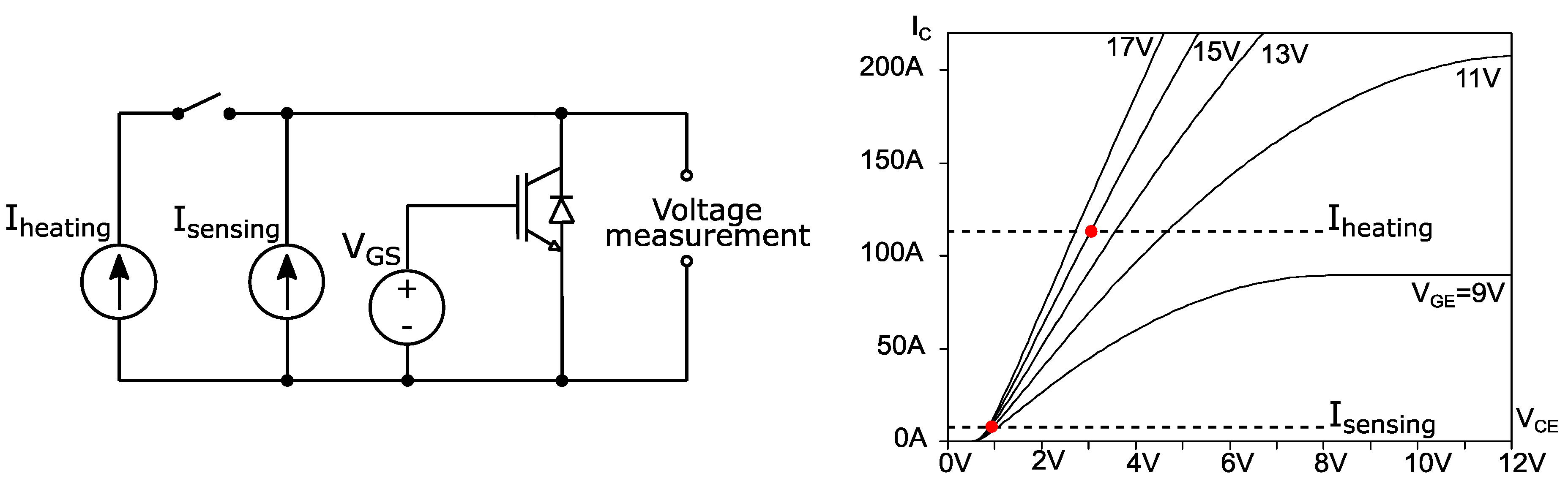
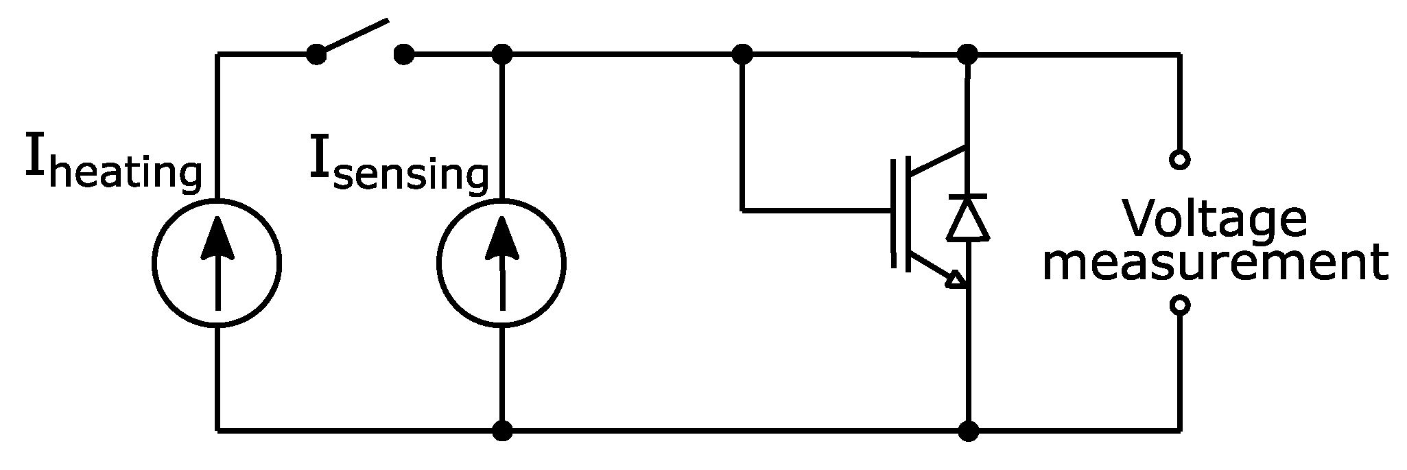
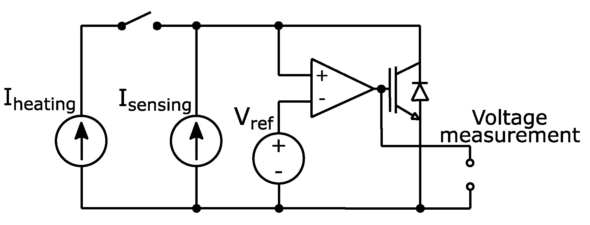
2.1. Electrical Setup

The process of power cycling is relatively simple. During the heating period, a heating power needs to be applied on the device as long as the device is heated up. Once the defined heating time ends, the heating must be switched off. In the cooling period, the device is not powered, and there might be only some minor biasing on the device to enable the measurement of the chip temperature. The repeated heating and cooling periods represent the power cycling.

2.1.1. Current or Voltage Driving

The first aspect that needs to be considered is how the heating power is applied on the module. As a reference, we can take a look at the real application conditions. Most of the power modules are used in switching mode power converter applications where the transistors are used to switch the current of a load impedance either on or off, with relatively high frequencies. The dissipation is generated by the switching losses and the conduction losses. Let us consider the conduction losses first. In the off state, the transistor is in high impedance mode, there is a high voltage drop on the device, but no current is flowing through it, hence there is no power dissipation. Conduction losses are generated when the transistor is on. In this state, the current flowing through the transistor is defined by the load impedance and the supply voltage, and is practically independent of the transistor itself. In laboratory conditions, using a voltage source and a serially connected load impedance would dissipate the majority of the applied power and make the test inefficient. It is more efficient to simply use a constant current source for driving the module.

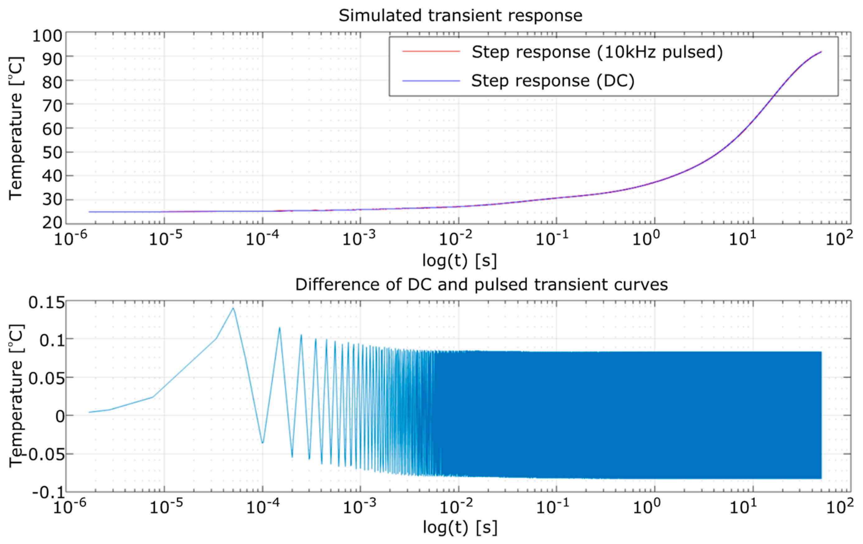
2.1.2. Pulsed or Direct Current (DC) Driving

Switching losses are generated when the transistors change state, either turn on and off. During this very short transient duration, the voltage and current can be simultaneously high, resulting in a huge peak dissipation for a very short time. Switching losses are dependent on the supply voltage, the on-state current, and on the parasitic capacitances and stray inductance of the structure [22], besides some other, less important parameters. If the power-cycling system needs to utilize the switching losses, a high supply voltage and a realistic load impedance would be required, which would again make the system overcomplicated and inefficient. Although both the switching losses and the conduction losses are only present in a small part of the full cycle, the smallest time constants of the thermal response of the chip do not allow us to follow the very quick changes, hence only the average dissipation will have a significant effect on the temperature. As a result, applying the heating on the device with a constant current load utilizing only the conduction losses would only cause a marginal loss of accuracy. The difference can be examined, e.g., with a SPICE simulation [23], as demonstrated below.
For demonstration purposes, a 600 A, 1200 V IGBT module was selected. Each IGBT device consisted of 4 parallel IGBT chips mounted on a DCB. The time-domain thermal behavior of one IGBT switch was measured using thermal transient testing [24] and modeled with a 5 stage RC network (Cauer topology). The schematic of the simulated topology can be seen in Figure 2 and the used component parameters can be found in Table 1.
Transient simulations were run in a SPICE simulator with pulsed (10 kHz, 50% duty cycle) and DC loads with identical average power. The heating power was selected to reach an approximately 100 °C temperature change, for easy handling. The simulated transients are shown in Figure 3, in the top diagram. It can be seen that it is hard to differentiate the red (pulsed powering) and blue (DC powering) curves. In the bottom diagram, the difference of the simulated transients is plotted. The difference was below 0.2 °C, which was about 0.2% of the overall temperature change. The simulation model could be further refined, but this result already demonstrates that simple constant current heating can be used for powering, with a negligible loss of accuracy.
During the power-cycling experiment, the most obvious monitoring parameters were the electrical properties. These parameters could be measured without interrupting the test operation. As the device electrical characteristics were temperature-dependent, the constant current load on the device enabled us to capture the temperature-dependent forward voltage drop (VCE, VDS, VF, depending on the component type and the electrical setup). After proper calibration of its temperature dependence, this voltage drop could be used to calculate the junction temperature of the component. However, the serial resistance of the module could change during the power cycling; at a small sensing current level, this only had a negligible effect on the voltage drop on the device. If the change of the device characteristic was assumed, the temperature sensitivity calibration might need repeating in those cases where a significant change in temperature was experienced, in order to validate the temperature readings.

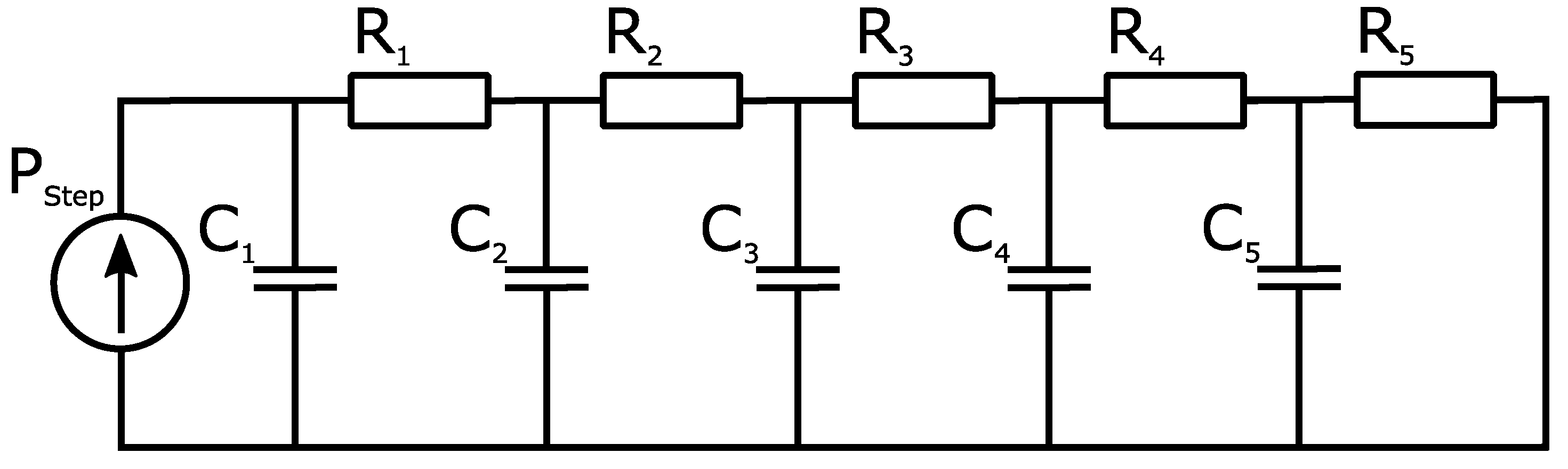
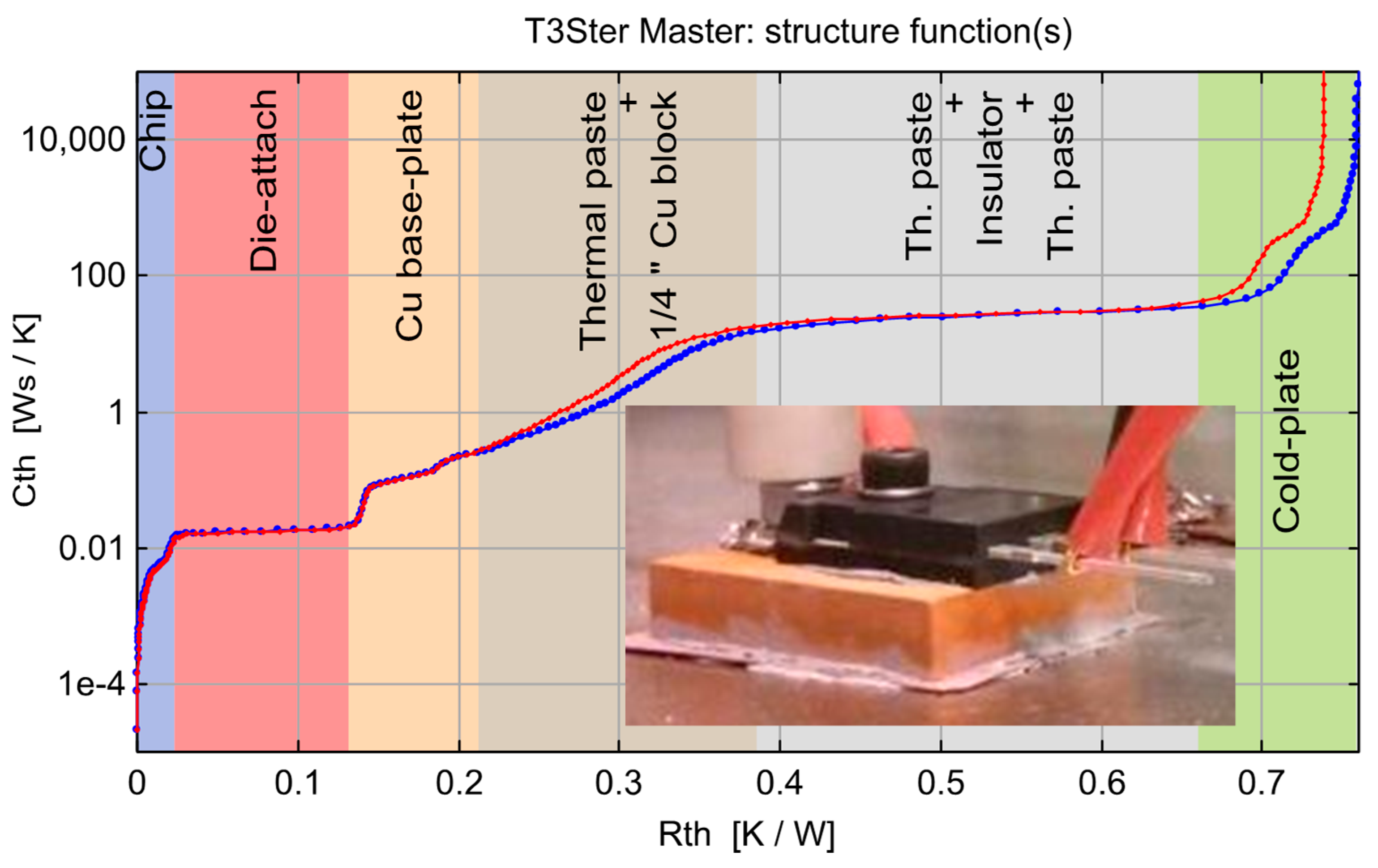
2.2. Thermal Transient Measurement and Electrical Schemes

The temperature sensitivity of the voltage drop on IGBT, MOSFET, and diode devices was low, it was usually in the range of a few mV/°C (about 2 mV/°C for a pn-junction). Although the device voltage was temperature-dependent at high current levels as well, if the heating current was provided by a switching mode power supply, the current and voltage fluctuation made the temperature measurement inaccurate. The junction temperature could be measured more accurately by using only a small sensing current, provided by a linear current generator, when the heating current was turned off. As the device voltage started to decrease exponentially, right after switching off the heating power, the first measurement point needed to be captured as soon as possible. In order to compensate the delay between the first measurement point and the time of the switching, the maximum junction temperature was usually calculated by fitting a square root curve on the initial section of the captured cooling curve and was extrapolated back to the moment of switching [25]. In order to minimize the inaccuracy introduced by the extrapolation and achieve an accurate junction temperature measurement, the voltage measurement needed to have high resolution, both in terms of voltage and time.
If not only the minimum and maximum temperatures were measured but the whole heating or cooling transient of the junction was captured after a stepwise change in the applied power dissipation, then the obtained function was called the thermal transient curve of the component [24]. The thermal transient curve was dependent on the heat flow path, i.e., the structure and the material parameters of the device packaging, hence, it carried information about these parameters. With appropriate post-processing of the thermal transients, the structure along the heat flow path could be examined [26]. Comparing the structural information obtained with this method during the progress of the power cycling to the one captured in the initial state at the start of the test, structural degradation could be indicated. This method is discussed in Section 3.1, in more details.
During heating, a constant current was applied on the component, but capturing the thermal transient in this state was not recommended, as the measured signal contained significant electrical noise. The electrical noise made accurate voltage measurement impossible without averaging, which would compromise the time resolution of the temperature data. The calibration of the temperature sensitivity was also challenging, as it required controlling the junction temperature by regulating the environmental temperature. In the high-current load state, this required a high cooling power, and in addition, the junction temperature significantly differed from the environmental temperature, through an unknown offset.
For these reasons, capturing the cooling transient of the device was easier and more accurate. To do this, however, the device needed to be kept operational during cooling, by applying a small so-called sensing current.
There are multiple electrical setups, which enable increasing the probability of certain failure modes.
The on-state conduction loss of the IGBT could be used for heating, using the electrical setup shown in Figure 4 (left panel). The device was fully turned on by an appropriate gate voltage, and a constant current source provided the heating current (Iheating). An additional Isensing constant current source was also connected to the device and this current was connected even if the Iheating was switched-off. The resulting operating points are highlighted on the typical IGBT characteristic curve shown in Figure 4 (right panel). This setting enabled measuring the VCE forward voltage of the IGBT and hence calculating the junction temperature. This electrical setup strongly resembled the usual application conditions, consequently it was optimal for lifetime estimations. However, by eliminating the switching losses, a higher current was required to achieve the desired temperature changes. This elevated current put excess load on the bond wires. For this reason, this setup could be optimal for focusing on bond-wire testing, especially by using short cycle times, not leaving time for the further layers to heat up to the maximum steady-state temperatures.
The current load could be limited by slightly decreasing the gate voltage and increasing the VCE voltage drop, consequently.
If the intention was to compare different die-attach or baseplate soldering technologies and not to do lifetime estimation, it was beneficial to decrease the current load in order to protect the bond wires. A simple solution was to modify the electrical setup by connecting the gate of the IGBT (or MOSFET) to its own collector (drain), as shown in Figure 5. The resulting two pole configurations had a quadratic characteristic with a VCE (VGE) voltage that was equal to the threshold voltage of the transistor, at a low-load current. The threshold voltage showed significantly higher temperature dependence than the on-state forward voltage, enabling high accuracy junction temperature measurement.
This measurement setup needed to be handled carefully in case the modules contained multiple parallel chips, forming a single switch. Due to the negative temperature dependence in this state, even a slight difference in the device characteristics between the chips (e.g., difference in threshold voltage) could result in a higher load on one of the chips, leading to a reduced lifetime or even to a thermal runaway.
A more sophisticated control of the voltage drop could be achieved by implementing an active feedback loop between the collector voltage and the gate voltage. The setup shown in Figure 6 used an active circuit to control the gate voltage so that the VCE voltage was kept equal to a reference voltage (Vref), independent of the load current. Using this circuit, the transistor’s voltage and current could be controlled at the same time, enabling us to set any valid operating point. Although the gate voltage was the output of the control circuit, its value was dependent on the IGBT junction temperature hence could be used to capture the thermal transient of the component after an appropriate calibration. In the case of the parallel-connected chips, the optimal tradeoff between the load current and the device voltage could be programmed, limiting the risk of uneven power distribution within the package or a thermal runaway.
In the case of MOSFETs, the small serial resistance often made it impossible to use small sensor current to measure the chip temperature. To overcome this problem, the body diode could be used for power cycling. The on-state setup shown in Figure 4 could be used for the MOSFETs as well. However, the sensor current had to be negative and the gate voltage had to be switched off, for the duration of the cooling. In this mode, serial resistance was used for heating, and the body diode was used for accurate temperature measurement. The latter two setups could also be applied for MOSFETs, without any modifications.

3. Discussion

As discussed in the introduction, in the complex structure of power devices, several failure mechanisms can lead to the degradation of the operation. With the power-cycling testing, the degradation of the device was accelerated. We now propose a method to determine the origin of the degraded operation.

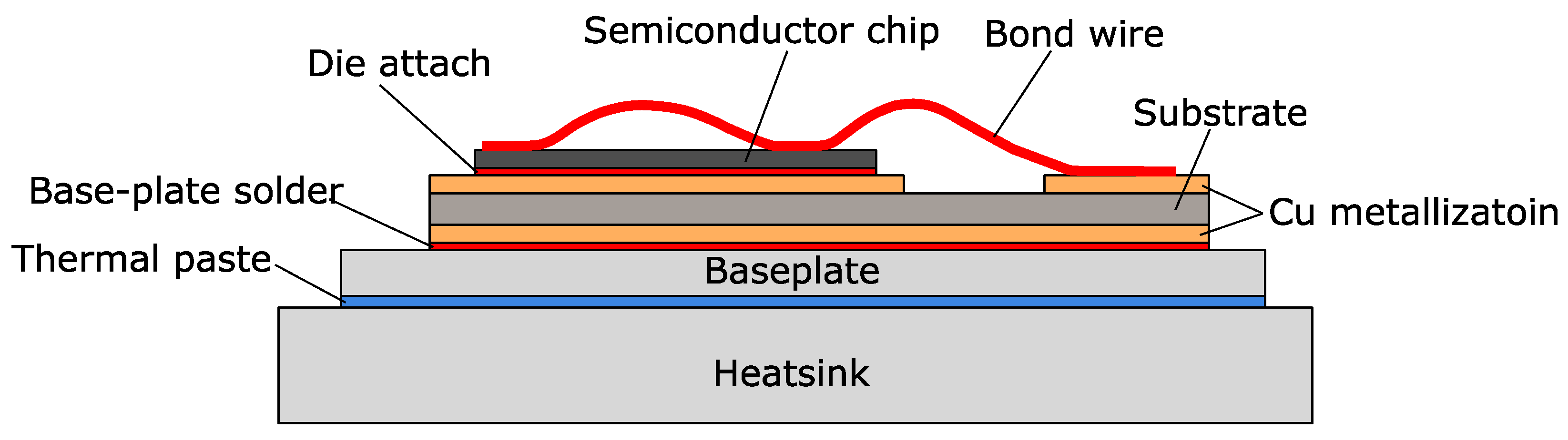
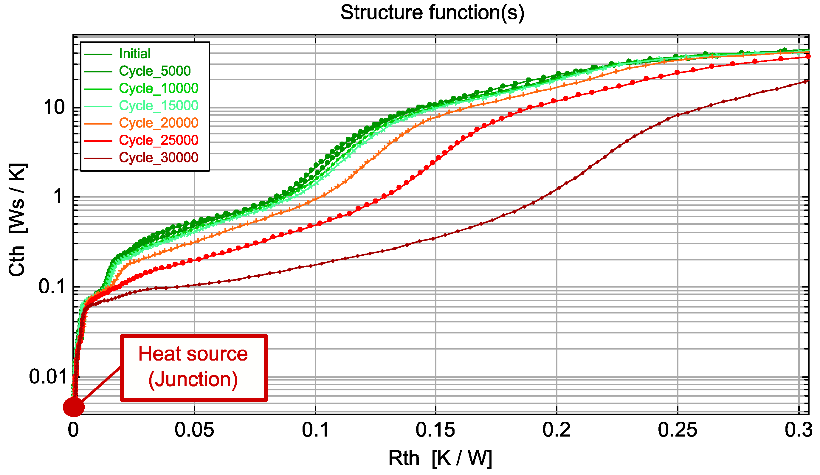
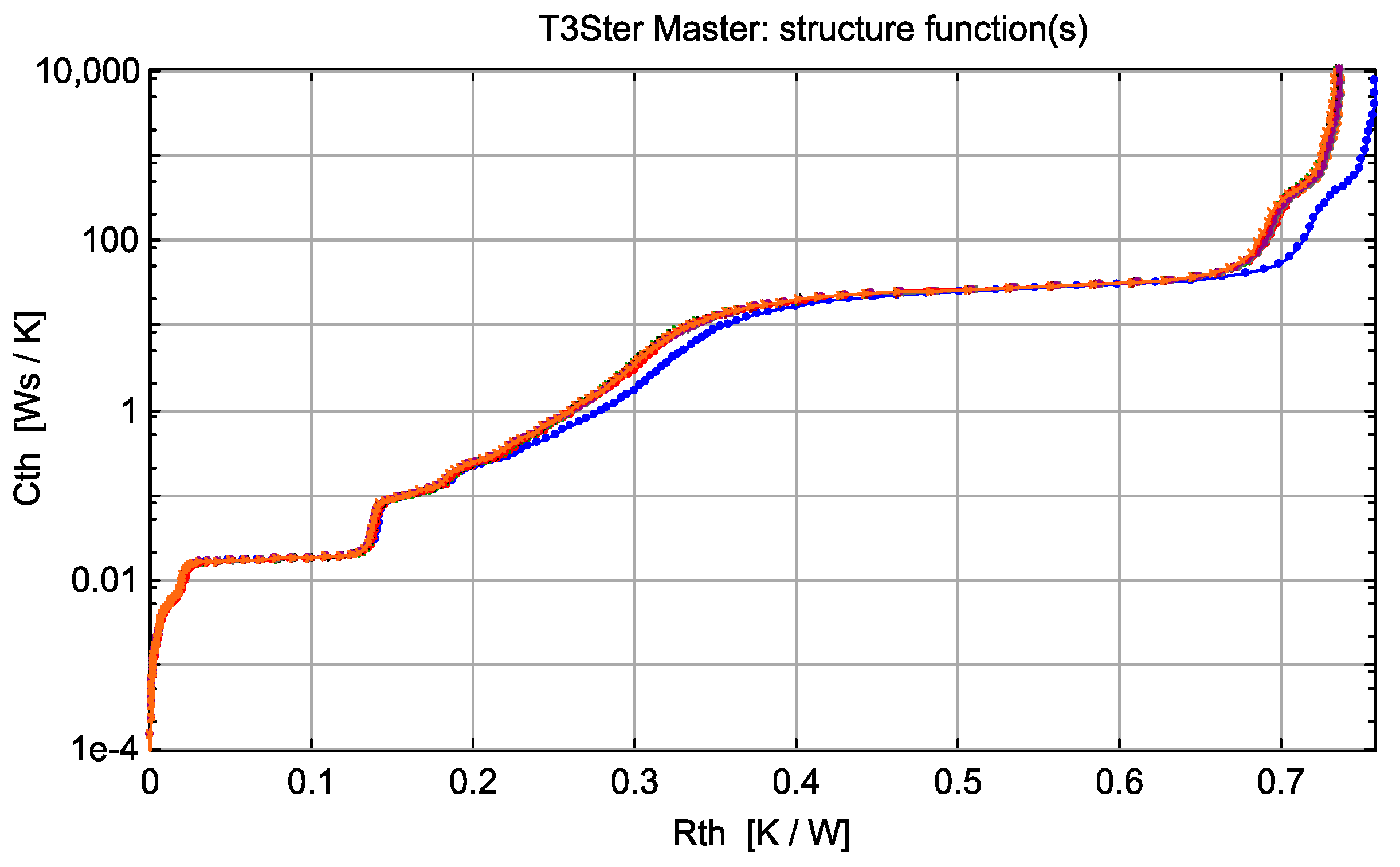
3.1. Structure Degradation in the Heat Flow Path

The most important failures in a power package originated from the degradation of the interface materials. When the interface material was the die-attach material, the failure was called a die-attach failure, when the degraded interface was the soldering, the failure was called TIM2 failure. The third ageing-related failure in power packages was the bond-wire degradation.
In this chapter, we present how these failure modes could be identified during power-cycling tests.

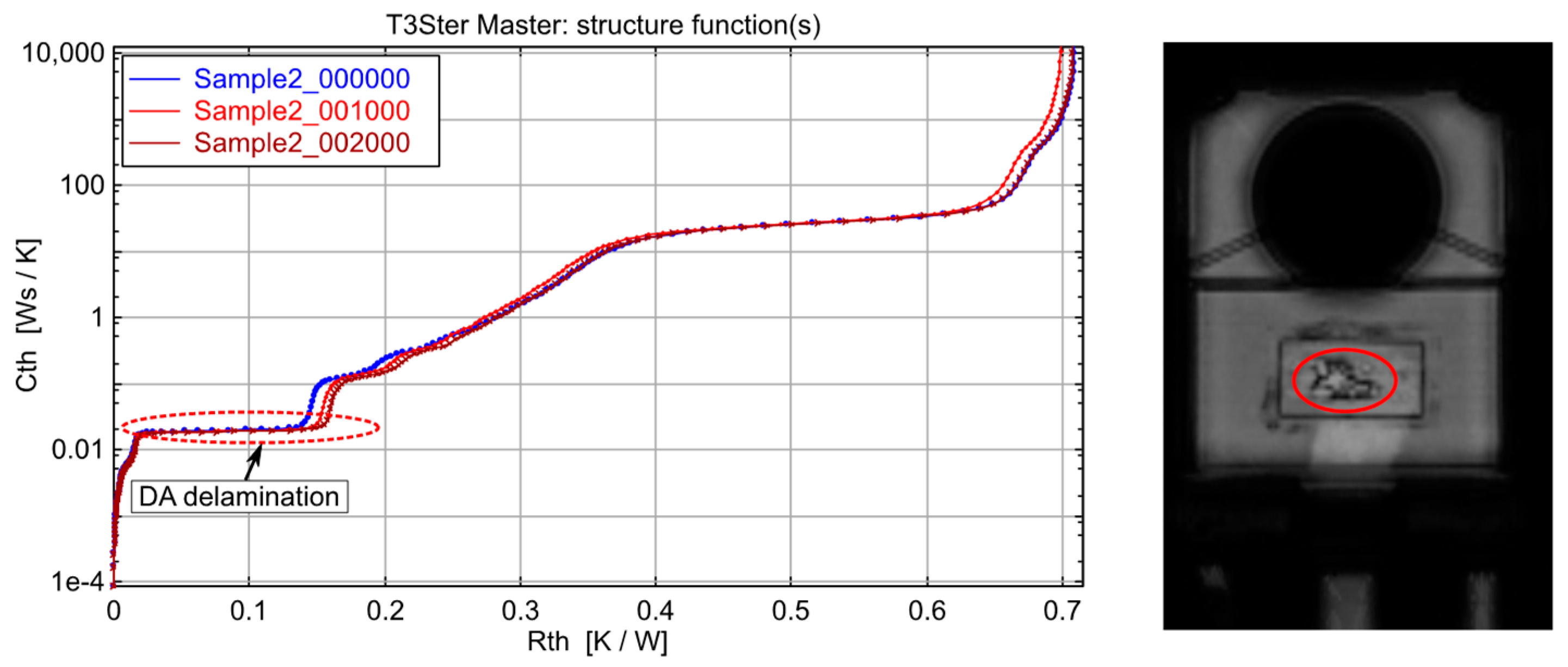
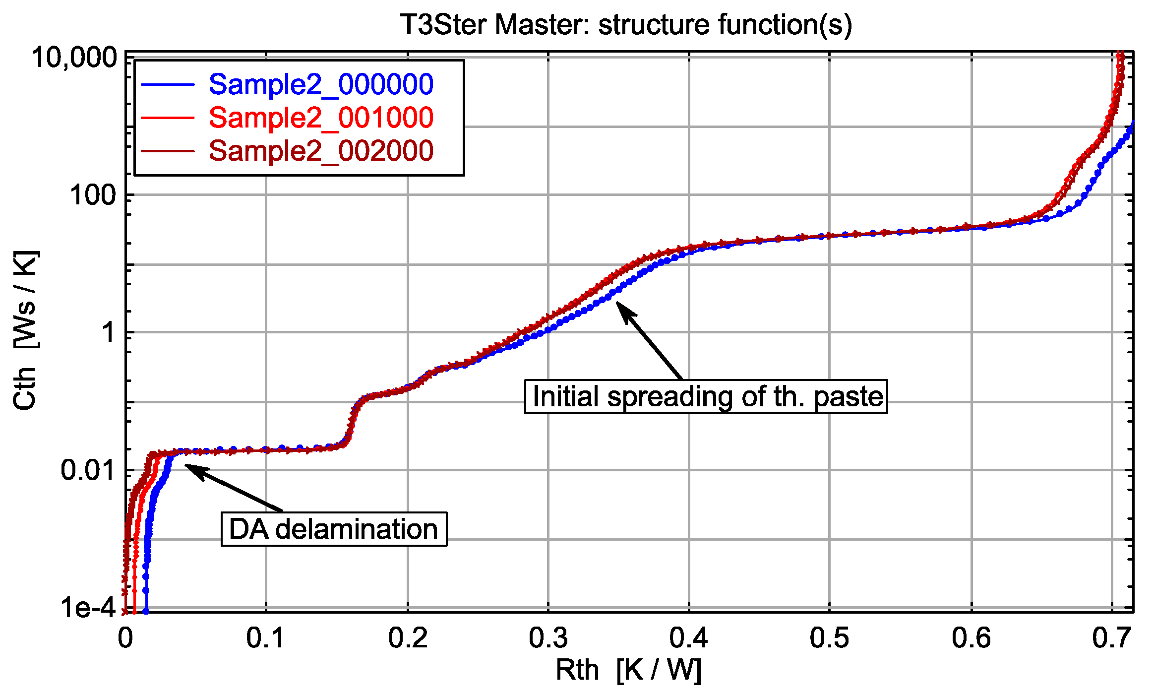
3.1.1. Die-Attach Degradation

The behavior of thermal systems is often described by using the electric equivalent circuit, as was already shown in the SPICE simulation example in Section 2.1. The heat storage capability of a volume was described by the Cth thermal capacitance and the resistance to the heat flow was represented by the Rth thermal resistance. As the heat passed through the various layers, the thermal capacitances and thermal resistances of the structure defined the pace of the temperature change.
The power-cycling setups discussed above were constructed to enable capturing the cooling transient of the junction temperature, through some temperature-dependent electric parameters (different in each setups). This transient curve could be transformed into a one-dimensional RC model of the heat flow path [8]. If the model was transformed into the Cauer form, the model parameters had physical meaning. The thermal capacitance (Cth) was proportional to the volume and specific heat of the material layers where the heat passed through and the thermal resistances (Rth) were proportional to the conductivity and the cross-sectional area of the layers. The (cumulative) structure function was a visual representation of this RC network, by plotting the sum of the thermal capacitances in the model, as the function of the sum of thermal resistances. This representation could be used to find the source of the degradation if the structure changed [27].
In Figure 7, the structure functions generated from the cooling transient measurements can be seen. The model parameters were calculated using the deconvolution-based network model identification method discussed in [28]. The highest values (dark green curve) represent the initial state and the subsequent curves show the structure functions, after various number of power cycles. The power-cycling setup and parameters were selected to focus on the die-attach reliability. An 80 A IGBT module was tested using the threshold mode setup at elevated voltage levels (see Section 2.2). The device package was fixed to a water-cooled cooling plate with the coolant temperature set to 25 °C. The junction temperature change was set to 100 °C, and the heating power was maximized to achieve the peak temperature in a short time. The heating current was 25 A and the heating and cooling time was 3 and 13 s, respectively.
Thermal transient curves were captured after every 200 load cycles. As the failure formation was slow, the structure functions generated only after every 5000 cycles are plotted in Figure 7. It can be seen that up to about 15,000 cycles all curves fit well, the differences could only be attributed to the uncertainty of the measurement. The overlapping of the curves shows that the structure was intact and the measurement was highly repeatable. The curve corresponding to 20,000 cycles, however, started to differ and the differences further increased significantly in the subsequent measurements as well. The position of the separation point marked the location of the degradation. The first steep section corresponded to the high capacitance to the resistance ratio of the chip itself. The separation happens in the following layer, which is the die-attach. The change of the slope and the elongation of the section showed the increase of the die-attach resistance, probably due to a crack propagation. The tested device finally failed after about 35,000 cycles, but this internal degradation could already be detected at half the lifetime.

3.1.2. Baseplate Solder (TIM 2) Degradation

As shown in the previous example, the various layers in the structure could be correlated to the sections on the structure function. The structure function always started in the origin and ended with a singularity (vertical section) representing the practically infinite thermal capacitance of the ambient. Between the two ends, the slope of the curve carried information about the added capacitance and the resistance of each layer. A steep section represented a material that had a high thermal capacitance and a low thermal resistance, which was a good conducting material, while a flat section corresponded to a poor heat conductor material (or narrow geometry). In typical semiconductor structures, the two type of layers are arranged one after the other, enabling us to roughly identify the layers, as shown below.
In Figure 8, the structure functions corresponding to a SiC MOSFET in a TO-247 style package and the photo of the measured structure can be seen. The device and test parameters are summarized in Table 2. The various sections of the curve were identified and marked with different background colors. As the heat receded from the chip, the 3D heat spread became even more significant, making it more difficult so separate the adjacent layers. In order to help identify the various sections, multiple measurements could be carried out by intentionally changing the structure to a slight extent. This method is often used to measure, for example, the junction-to-case thermal resistance [29].
The two curves in Figure 8 correspond to the same device, but were measured with two different thermal interface materials (TIM) between the package-cooling surface and the copper block. The separation point around 0.23 K/W helped identify the boundary between the baseplate of the transistor and the TIM material under it. The second separation point at 0.65 K/W was the result of the increased thermal resistance of the TIM material as well (the increased TIM resistance shifted the whole curve above the first separation point to the right) and thus could be ignored.
After the initial characterization, a power-cycling test was done on a set of devices similar to the one discussed before. In order to reduce the bond-wire failure probability, the threshold mode was used for this experiment as well. A 22 A load current was applied with 10 s on and 10 s off times, to achieve an about 95 °C junction-temperature swing.
In Figure 9, the structure functions corresponding to Sample 1 can be seen. The blue curve was captured before the first load cycle, while the other curves were captured after every 1000 cycles. Only the blue curve was different, all the others fit perfectly at every Rth value; these are barely visible in the figure. An interesting effect was observed here, as in the first cycle, the overall thermal resistance was higher, it was reduced in the initial part of the power cycling, and no change was visible after the first 1000 cycles. The separation of the curves happened right at the thermal resistance value of 0.2 K/W. With the help of the layer identification in Figure 8, we could conclude that the change happened in the TIM material between the package and the copper block. The initial change was probably the result of spreading and thinning of the thermal paste, due to the elevated temperature and the pressure.
Taking a look at the structure functions of Sample 2 in Figure 10, on the left hand side diagram, a similar plot can be seen, but the separation of the curves happened much earlier. The separation point at 0.14 K/W was the result of the elongation of the previous, almost perfectly flat section, corresponding to the die-attach resistance. The scanning acoustic microscopy image (C-SAM) captured from the backside and focused to the die-attach layer confirmed the die-attach problem (shown in Figure 10 on the right). After about 0.25 K/W, however, all curves ran together again.
Selecting an appropriate feature in the structure after the degraded layer and fitting the curves at the corresponding section could also help analyze also the further sections. On the right hand side diagram in Figure 11, the curves were shifted horizontally to overlap at the section that corresponded to the copper base-plate of the device. This was a well-defined capacitance step on the curves. This fitting revealed the same type of change in the section corresponding to the first TIM layer that we saw in the case of Sample 1 (Figure 9) as well. Using this method, the concurrently arising failure modes could be separated and analyzed individually.

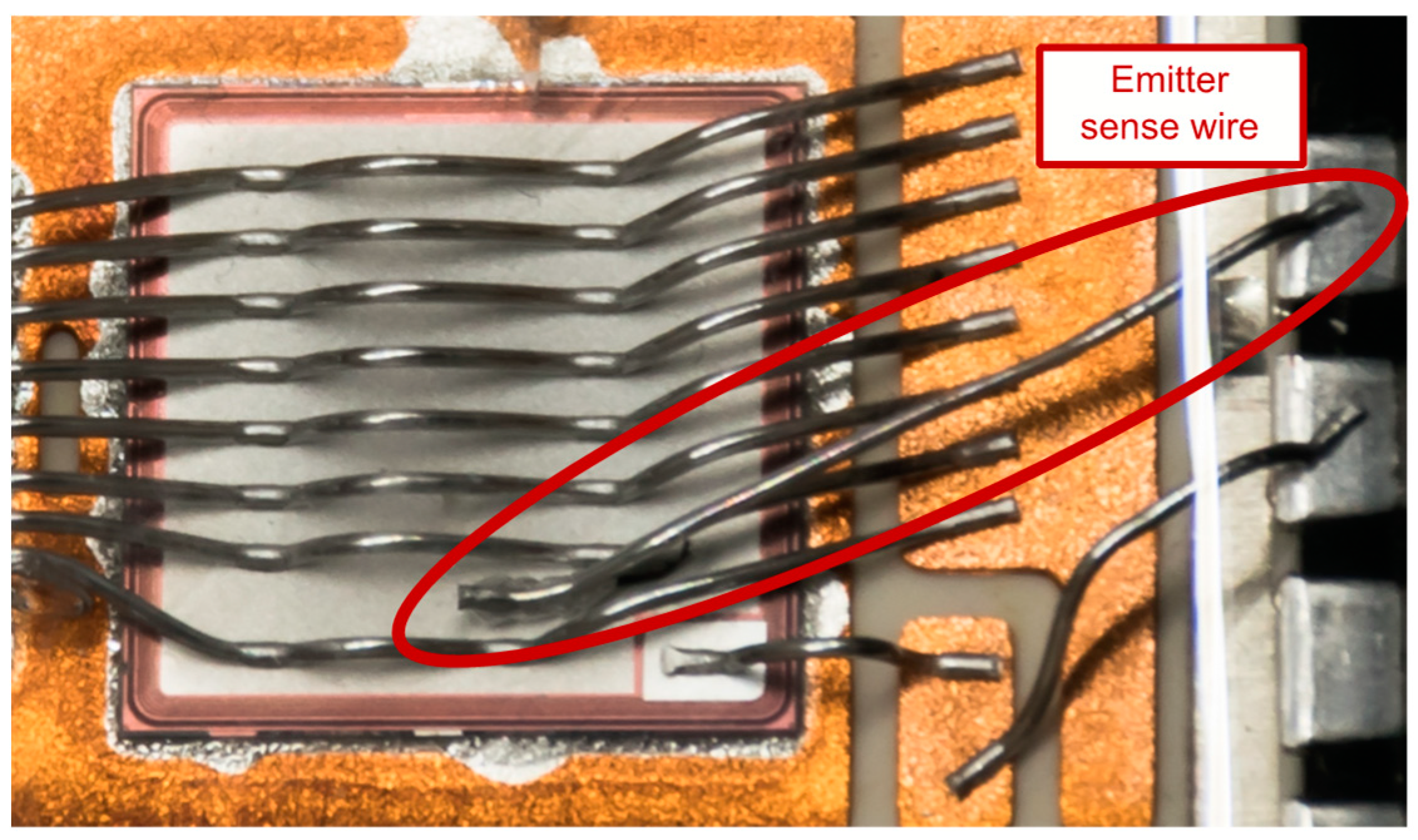
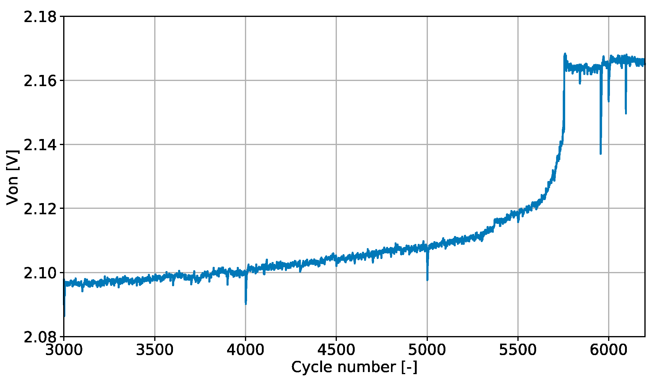
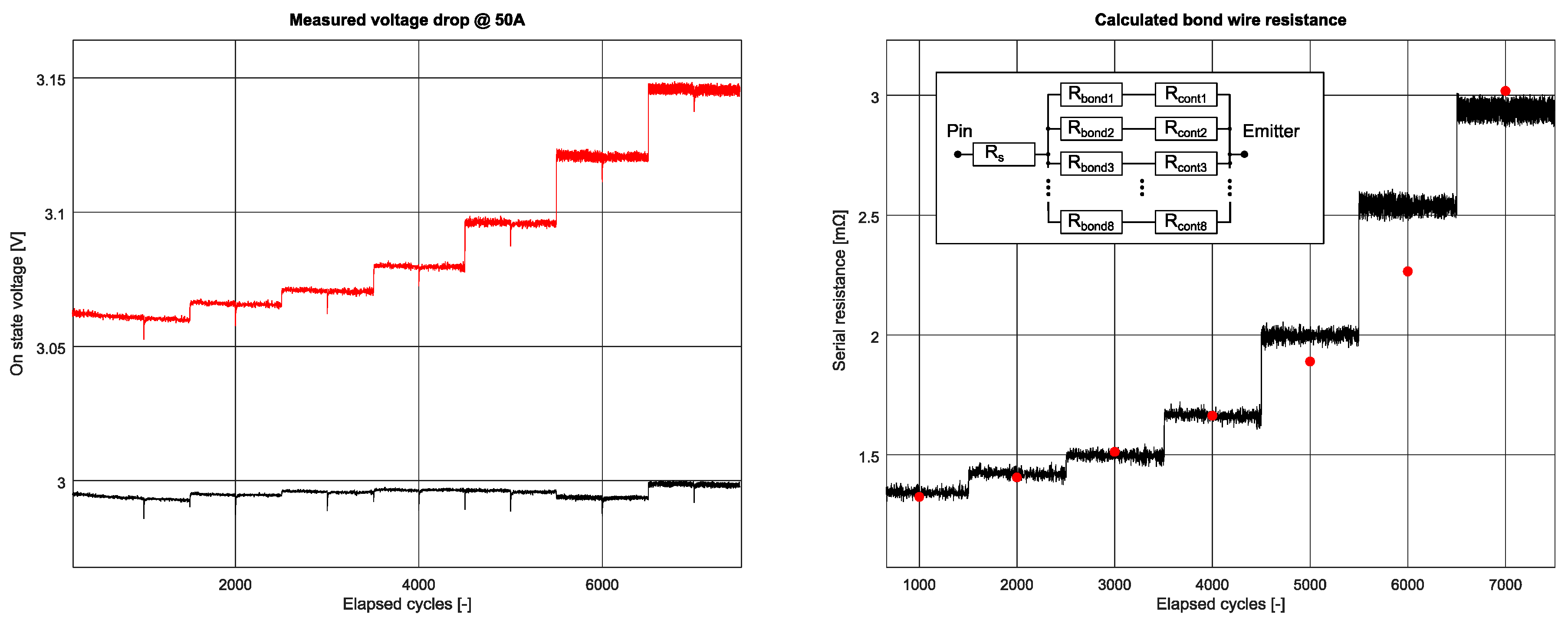
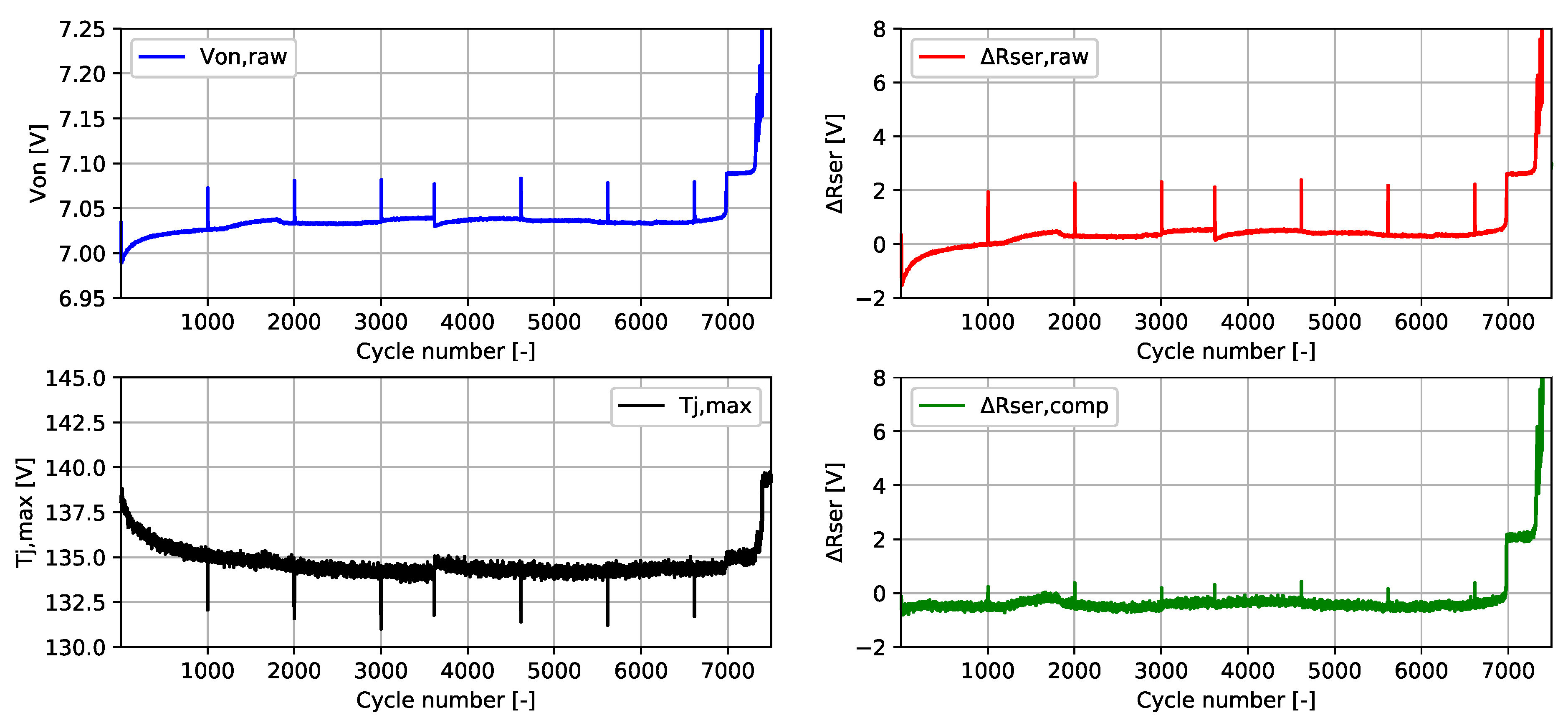
3.2. Bond-Wire Degradation and Separation of the Effects

As the bond-wire degradation did not contribute significantly to the cooling of the chip (it was not part of the heat-flow path), its integrity could not be investigated using the captured thermal transient curves. However, an accurate voltage measurement could detect the small changes in the device voltage caused by the increasing serial resistance, represented by the damaged bond wires. Some high-power modules contain dedicated bond wires for controlling the transistor (as can be seen in Figure 12), but in order to monitor the bond wires we need to make sure that the voltage measurement probes were connected to the high current inputs of the module. As the cumulative resistance of the bond wires was very low, the voltage drop needed to be measured when the heating current was applied on the device.
In the following experiments, the same type of module was used as the one shown in Section 3.1.1, with its parameters summarized in Table 3. The IGBT device was tested in the on-state with 100A load current slightly above its current rating, in order to facilitate the bond-wire degradation. The voltage drop across the components was captured in each cycle at the end of the heating period before the heating current was switched off. In Figure 13, the collector emitter voltage is shown in the function of the number of applied power cycles. In this plot, we magnified only on a small section where a stepwise change in the voltage drop could be identified. In the first section of the curve until about 5500 cycles, a gradually increasing tendency can be seen, which could most likely be attributed to the aluminum reconstruction on the chip surface, followed by a crack propagation in the bond or at the bond-wire-to-chip interface [30].
After about 5500 cycles, the speed of the degradation increased until finally a stepwise change was visible. This stepwise change corresponded to the breakage or detachment of one of the parallel bond wires. After the voltage step, the slope of the curve became relatively flat again until the next bond wire failed. The outlying points in the curve show the location of the control measurements.
In order to validate that the above interpretation of the stepwise voltage change was valid we created an experimental setup. The advantages of this module were the easy to remove cover and a dedicated sense pin connected to the chip surface, with a dedicated bond wire. We applied a gate voltage to open the IGBT fully and connected it to the Ch1 and Ch2 measurement channels of a thermal transient tester, as shown in Figure 14. We started a power-cycling test with a sufficiently low load current to make sure that the bond wires had no thermally induced degradation during the test. The resulting junction temperature swing was as low as 35 °C.
We started the power cycling, and measured the voltage drop on both measurement channels in each cycle, as described above. Thanks to the removable top cover of the module, we had direct insight into the module. The IGBT chips emitters were connected by eight individual bond wires. We let the cycling run for a few hundred cycles to make sure that the device voltage was stable, then using a pair of pinchers we started to cut the individual bond wires, one after the other in every thousand cycles to check the effect in the measured voltages. The measured voltages are shown in Figure 15, on the left side diagram, as the function of the power cycles. As there was only artificial bond-wire degradation, the voltage measured on Channel 2 (black curve) used the dedicated sense pin and hence excluded the voltage drop on the bond wires, which showed no significant change during the test. In contrast, on Channel 1 (red curve), the measured voltage increased in steps as we cut the bonds.
By subtracting the two voltages and dividing it by the load current, the equivalent serial resistance could be calculated for each cycles. The serial resistance is shown in the function of the power cycles in Figure 14; right plot, in black. We used a simple resistor network (also shown in Figure 14) to model the serial resistances, including the bond wires. We measured the length and diameter of the individual bond wires (12 and 1.35 mm, respectively), and calculated the bond-wire resistance. The remaining model parameters were selected to fit the model to the experimental results. By selecting 1 mΩ for contact resistance and 0.75 mΩ for additional serial resistance (Rs), a good match could be achieved, as is visible in the plot. The red dots represented the calculated serial resistances. Most calculated resistances fit well with the measured resistances, a higher difference could only be observed at 5000 and 6000 cycles, which were probably caused by the slightly different wire lengths and the variation in the contact resistances. The high current density could also have an effect on the bond-wire temperature, hence, changing their resistances, as well.
Normally, those wires that carry the high current are likely to fail. The gate-bond wires, however, are also in contact with the active surface and could also fail. If a gate-bond wire lifts off due to the gate capacitance, the device remains on for an indefinite time duration. This could remain unnoticed or cause strange effects. There is, however, a simple method for testing the gate bond wire continuity, by turning off the gate voltage in regular intervals and checking if the device goes into a high impedance state. If the device is still conducting, the test can be stopped with gate-bond failure.

3.2.1. Correction of the Von Voltage

During the power-cycling tests, bond wire and other structural degradations could occur concurrently, hence, the voltage drop on the device under test (DUT) could be affected by both factors. The measured voltage (Vm) could be expressed at any load current (I) and temperature (T) as the sum of the DUT voltage in such conditions (VD), plus the voltage drop on the serial resistance of the internal wiring between the sensing point and the chip surface (Rser), with the equation
V m ( I , T ) = V D ( I , T ) + R s e r I .
The on-state voltage is usually defined as the voltage drop measured on the device at the end of the heating pulse, just before the heating power is turned off. This voltage corresponds to the maximum device temperature (Tmax). During the power cycling, the structural degradation in the heat flow path increases the thermal resistance and consequently increases the maximum device temperature as well.
Considering this factor, the device voltage can be expressed as
V D ( I , T ) = V D ( I , T m a x , 0 ) + k ( I ) Δ T m a x , n
where Tmax,0 is the peak-junction temperature in the initial (good) state, k(I) is the temperature dependence of the device voltage at a certain load current, and ΔTmax,n is the change of the maximum junction temperature caused by the structural change, until cycle number n. The above equations are true, both, at the heating and sensing current levels. During cooling, a sensing current is applied on the device, which is usually a small current, often not more than a few tens or hundreds of milliamps. At the sensing current levels, the voltage drop on the serial resistance are negligible and hence the temperature dependence can be accurately characterized and the junction temperature can be calculated (both in hot and cold state). As a result, the change of the maximum junction temperature until cycle number n can be expressed as
Δ T m a x , n = k ( I s e n s e ) × ( V D , n V D , 0 ) .
Knowing the change of the maximum junction temperature and combining Equations (1) and (2), the serial resistance can be expressed as
Δ R s e r = V m ( I h e a t i n g , T m a x , n ) V m ( I h e a t i n g , T m a x , 0 ) k ( I h e a t i n g ) Δ T m a x , n I h e a t i n g .
In order to be able to evaluate this formula, the value of k(Iheating) needs to be known. Temperature sensitivity calibration is usually a simple process, the DUT needs to be put in a temperature-controlled environment, the desired biasing currents and voltages are applied, and the voltage drop is measured at different temperatures. The temperature sensitivity can be acquired from the measured voltages through curve fitting. In practice, however, the calibration at high current is rather challenging. The calibration environment must have high heat-sinking capability with an accurate temperature regulation capability. Moreover, the dissipation elevates the junction temperature and there is also an unknown voltage drop on the serial resistances.
A possible method to overcome this is to use the same junction-temperature measurement method as in power cycling. First, the temperature sensitivity of the device should be calibrated at the sensing current level. Then, at every temperature steps, a short heating cycle is applied on the device. The device voltage is registered at the end of the heating pulse. The corresponding temperature is unknown yet, but if the sensing current is applied on the device right after turning off the heating, the cooling of the device can be measured and by extrapolating back from the cooling curve to the moment of the switch off, the peak junction temperature can be calculated. This temperature and the registered voltage at the heating current can then be used to fit a calibration curve and calculate k(Iheating).
In Figure 16, the above shown temperature compensation method is demonstrated using a data set acquired on a SiC MOSFET device in To247 style package (same component as used in Section 3.1.2). In this experiment, the MOSFET device was connected in the threshold diode mode and cycled with a 27 A heating current at a 40 °C baseplate temperature. The voltage drop on the device is shown in the function of power cycles in the top left plot in blue and the corresponding peak-junction temperature is shown in the bottom left plot. In the early section of the cycling, the peak-junction temperature decreased significantly because of the spreading of the thermal interface material below the transistor package, resulting in an increasing device voltage (Von). Without using Equation (4) to compensate the effect of the temperature change, a strange (negative) serial resistance change was observed, as seen in the top-right plot in red. We calibrated the temperature sensitivity of the component at the heating current level and acquired a temperature sensitivity of −9.5 mV/°C. Using this value for the compensation, it could be observed in the bottom right plot in green that the strange initial resistance change could be completely eliminated and only a small variation remained.
Nowadays, in order to avoid the vulnerable bonding wires, the development of double-sided cooling packages have started as well. These new package structures provide additional heat flow paths that could potentially reduce the thermal resistance. At the same time, double-sided cooling eliminates wire-bonding technology with all its issues [2,31]. These new technologies require the further development of the reliability testing methodologies, including real-time failure monitoring. Despite all its advantages, the double-sided cooling is not widely adopted by the industry yet and the classic wire-bonding is still the primary contacting technology in power electronics packages.

4. Conclusions

In this study, we investigated the possibilities of combining thermal transient testing with power cycling reliability tests, in order to achieve better on-line monitoring of the internal degradations of power semiconductor modules.
The two most common failure modes of power semiconductor modules were the bond-wire damage and the degradation of the thermal interface layers. We found that both failure modes could be detected on-line, during a power-cycling test, using the measured voltage parameters of the devices.
We have shown how the regularly captured thermal transients could be used to identify die-attach or other thermal interface layer deterioration in the heat-flow path and demonstrated how the concurrently arising structural changes could be separated by fitting structure functions at easy, to identify sections of the curve.
We have demonstrated how the bond-wire cracking and lift-off could be detected with high-resolution voltage measurement at high current loads. We emulated the bond-wire breakage by cutting the bond wires with a pair of tweezers. This experiment proved that the step-wise behavior of the VCE voltage at the driving current indicated bond-wire failure. We could model the decreasing number of bond wires with a simple resistor network. The model showed a very good match with the measured results.
Both bond-wire and structural degradation were indicated by the change of the measured forward-voltage drop in the device. Finally, we proposed a simple numerical compensation, which could separate the change of the effective bond-wire resistance from the effect of temperature change with low additional effort.

Author Contributions

Z.S. carried out the experiments and simulations, analyzed the results, formulated the bulk of the paper, and designed the figures. M.R. provided the concept of the paper, confirmed the validity of the results and contributed to editing the final paper. Both authors have read and agreed to the published version of the manuscript.

Funding

Part of the research reported in this paper has been supported by the National Research, Development and Innovation Fund (TUDFO/51757/2019-ITM, Thematic Excellence Program) at BME.

Conflicts of Interest

The authors declare no conflict of interest.

References

  1. Wu, W.; Held, M.; Jacob, P.; Scacco, P.; Birolini, A. Investigation on the Long Term Reliability of Power IGBT Modules. In Proceedings of the International Symposium on Power Semiconductor Devices and IC’s: ISPSD’95, Yokohama, Japan, 23–25 May 1995; pp. 443–448. [Google Scholar] [CrossRef]
  2. Amro, R.; Lutz, J.; Rudzki, J.; Thoben, M.; Lindemann, A. Double-Sided Low-Temperature Joining Technique for Power Cycling Capability at High Temperature. In Proceedings of the 2005 European Conference on Power Electronics and Applications, Dresden, Germany, 11–14 September 2005. [Google Scholar] [CrossRef]
  3. Schutze, T.; Berg, H.; Hierholzer, M. Further improvements in the reliability of IGBT modules. In Proceedings of the Conference Record of 1998 IEEE Industry Applications Conference, Thirty-Third IAS Annual Meeting, St. Louis, MO, USA, 12–15 October 1998; Volume 2, pp. 1022–1025. [Google Scholar] [CrossRef]
  4. Liu, Y.; Irving, S.; Desbiens, D.; Luk, T.; How, N.S.; Kwon, Y.; Lee, S. Impact of the die attach process on power & thermal cycling for a discrete style semiconductor package. EuroSimE 2005. In Proceedings of the 6th International Conference on Thermal, Mechanial and Multi-Physics Simulation and Experiments in Micro-Electronics and Micro-Systems, Berlin, Germany, 18–20 April 2005; pp. 221–226. [Google Scholar] [CrossRef]
  5. Guth, K.; Mahnke, P. Improving the thermal reliability of large area solder joints in IGBT power modules. In Proceedings of the 4th International Conference on Integrated Power Systems, Naples, Italy, 7–9 June 2006; Available online: https://ieeexplore.ieee.org/document/5758032 (accessed on 25 April 2020).
  6. Czerny, B.; Lederer, M.; Nagl, B.; Trnka, A.; Khatibi, G.; Thoben, M. Thermo-mechanical analysis of bonding wires in IGBT modules under operating conditions. Microelectron. Rel. 2012, 52, 2353–2357. [Google Scholar] [CrossRef]
  7. Davis, R.I.; Sprenger, D.I. Methodology and apparatus for rapid power cycle accumulation and in-situ incipient failure monitoring for power electronics modules. In Proceedings of the 2014 IEEE 64th Electronic Components and Technology Conference (ECTC), Orlando, FL, USA, 27–30 May 2014; pp. 1996–2002. [Google Scholar]
  8. Forest, F.; Huselstein, J.J.; Faucher, S.; Elghazouani, M.; Ladoux, P.; Meynard, T.A.; Richardeau, F.; Turpin, C. Use of opposition method in the test of high-power electronic converters. IEEE Trans. Ind. Electron. 2016, 53, 530–541. [Google Scholar] [CrossRef]
  9. Schuler, S.; Scheuermann, U. Impact of Test Control Strategy on Power Cycling Lifetime. Proc. PCIM 2010, 57, 355–360. [Google Scholar]
  10. Baker, N. An Electrical Method for Junction Temperature Measurement of Power Semiconductor Switches. Ph.D. Thesis, Aalborg Universitet, Aalborg, Denmark, February 2016. [Google Scholar]
  11. Khatir, Z.; Carubelli, S.; Lecoq, F. Real-time computation of thermal constraints in multichip power electronic devices. IEEE Trans. Compon. Packag. Technol. 2004, 27, 337–344. [Google Scholar] [CrossRef]
  12. Kim, Y.S.; Sul, S.K. On-line estimation of IGBT junction temperature using on-state voltage drop. In Proceedings of the Conference Record of 1998 IEEE Industry Applications Conference, Thirty-Third IAS Annual Meeting (Cat. No.98CH36242), St. Louis, MO, USA, 12–15 October 1998; Volume 2, pp. 853–859. [Google Scholar]
  13. Schmidt, R.; Scheuermann, U. Using the chip as a temperature sensor—The influence of steep lateral temperature gradients on the Vce(T)-measurement. In Proceedings of the 2009 13th European Conference on Power Electronics and Applications, Barcelona, Spain, 8–10 September 2009; pp. 1–9. [Google Scholar]
  14. Ogawa, E.; Nakayama, T.; Yoshida, S.; Takenoiri, S.; Ewald, S.; Otsuki, M. Ultra-high accuracy on-chip temperature sensor in RC-IGBT module for xEV, PCIM Europe 2019. In Proceedings of the International Exhibition and Conference for Power Electronics, Intelligent Motion, Renewable Energy and Energy Management, Nuremberg, Germany, 7–9 May 2019; pp. 1–4. [Google Scholar]
  15. Schmidt, R.; Scheuermann, U. Separating Failure Modes in Power Cycling Tests. In Proceedings of the 2012 7th International Conference on Integrated Power Electronics Systems (CIPS), Nuremberg, Germany, 6–8 March 2012; pp. 1–6. [Google Scholar]
  16. Musallam, M.; Yin, C.; Bailey, C.; Johnson, M. Mission Profile-Based Reliability Design and Real-Time Life Consumption Estimation in Power Electronics. IEEE Trans. Power Electron. 2015, 30, 2601–2613. [Google Scholar] [CrossRef] [Green Version]
  17. Ciappa, M. Lifetime prediction on the base of mission profiles. Microelectron. Reliab. 2015, 45, 1293–1298. [Google Scholar] [CrossRef]
  18. Standard Practices for Cycle Counting in Fatigue Analysis, ASTM E1049-85. 2017. Available online: https://www.astm.org/Standards/E1049 (accessed on 21 May 2020).
  19. Musallam, M.; Johnson, M. An Efficient Implementation of the Rainflow Counting Algorithm for Life Consumption Estimation. Reliability. IEEE Trans. Reliab. 2012, 61, 978–986. [Google Scholar] [CrossRef]
  20. Miner, M.A. Cumulative Damage in Fatigue. J. Appl. Mech. 1945, 67, A159–A164. [Google Scholar]
  21. Fatemi, A.; Yang, L. Cumulative fatigue damage and life prediction theories: A survey of the state of the art for homogeneous materials. Int. J. Fatigue 1998, 20, 9–34. [Google Scholar] [CrossRef]
  22. Feix, G.; Dieckerhoff, S.; Allmeling, J.; Schonberger, J. Simple methods to calculate IGBT and diode conduction and switching losses. In Proceedings of the 2009 13th European Conference on Power Electronics and Applications, Barcelona, Spain, 8–10 September 2009. [Google Scholar]
  23. Menhart, S. Using SPICE to calculate MOSFET operating temperature PESC ’92 Record. In Proceedings of the 23rd Annual IEEE Power Electronics Specialists Conference, Toledo, Spain, 29 June–3 July 1992; pp. 901–906. [Google Scholar] [CrossRef]
  24. Szekely, V.; Torok, S.; Nikodemusz, E.; Farkas, G.; Rencz, M. Measurement and evaluation of thermal transients, IMTC 2001. In Proceedings of the 18th IEEE Instrumentation and Measurement Technology Conference. Rediscovering Measurement in the Age of Informatics (Cat. No.01CH 37188), Budapest, Hungary, 21–23 May 2001; Volume 1, pp. 210–215. [Google Scholar] [CrossRef]
  25. Herold, C.; Beier, M.; Lutz, J.; Hensler, A. Improving the accuracy of junction temperature measurement with the square-root-t method. In Proceedings of the 19th International Workshop on Thermal Investigations of ICs and Systems (THERMINIC), Berlin, Germany, 25–27 September 2013; pp. 92–94. [Google Scholar]
  26. Rencz, M.R.; Szekely, V. Measuring partial thermal resistances in a heat-flow path. IEEE Trans. Compon. Packag. Technol. 2002, 25, 547–553. [Google Scholar] [CrossRef] [Green Version]
  27. Farkas, G.; Sarkany, Z.; Rencz, M. Structural Analysis of Power Devices and Assemblies by Thermal Transient Measurements. Energies 2019, 12, 2696. [Google Scholar] [CrossRef] [Green Version]
  28. Szekely, V. Identification of RC networks by deconvolution: Chances and limits. IEEE Trans. Circuits Syst. I Fundam. Theory Appl. 1998, 45, 244–258. [Google Scholar] [CrossRef]
  29. Schweitzer, D.; Pape, H.; Kutscherauer, R.; Walder, M. How to evaluate transient dual interface measurements of the Rth-JC of power semiconductor packages. In Proceedings of the 2009 25th Annual IEEE Semiconductor Thermal Measurement and Management Symposium, San Jose, CA, USA, 15–19 March 2009; pp. 172–179. [Google Scholar] [CrossRef]
  30. Ciappa, M.; Malberti, P. Plastic-strain of aluminium interconnections during pulsed operation of IGBT multichip modules. Qual. Reliab. Eng. Int. 1996, 12, 297–303. [Google Scholar] [CrossRef]
  31. Schneider-Ramelow, M.; Baumann, T.; Hoene, E. Design and assembly of power semiconductors with double-sided water cooling, Integrated Power Systems (CIPS). In Proceedings of the 5th International Conference on Integrated Power Electronics Systems, Nuremberg, Germany, 11–13 March 2008; pp. 1–7. Available online: http://ieeexplore.ieee.org/stamp/stamp.jsp?tp=&arnumber=5755676&isnumber=5755665 (accessed on 25 April 2020).
Figure 1. Cross-section of an insulated gate bipolar transistor (IGBT) module including the connected heatsink.
Energies 13 02718 g001
Figure 2. Four-stage Cauer topology RC thermal network representation of the IGBT device used for the transient simulation.
Energies 13 02718 g002
Figure 3. Simulated thermal responses with pulsed and DC driving.
Energies 13 02718 g003
Figure 4. On-state power-cycling setup (left), and the set operating points at a selected VGE, Isensing and Iheating combination (right).
Energies 13 02718 g004
Figure 5. Threshold (MOS diode) mode power-cycling setup.
Energies 13 02718 g005
Figure 6. Regulated VCE mode power-cycling setup.
Energies 13 02718 g006
Figure 7. Structure functions of the IGBT sample corresponding to the initial status and to the control measurements captured during the test.
Energies 13 02718 g007
Figure 8. Structure functions of Sample 1, with the structural layers identified.
Energies 13 02718 g008
Figure 9. Structure function of Sample 1 in the initial state (blue) and after every 1000 cycles (red, black, etc., overall 9 curves).
Energies 13 02718 g009
Figure 10. Structure function of Sample 2 in the initial state (blue) and after every one thousand cycles (red, brown.), in the original position (left) and the C-SAM image of the die-attach layer (right).
Energies 13 02718 g010
Figure 11. Structure function of Sample 2 in the initial state (blue) and after every one thousand cycles (red, brown) shifted right to fit at base-plate capacitance step.
Energies 13 02718 g011
Figure 12. Photo of an IGBT chip in a power module with a dedicated pin and bond wire for emitter voltage sensing directly on the chip surface.
Energies 13 02718 g012
Figure 13. Change of device voltage (VCE) at bond wire break.
Energies 13 02718 g013
Figure 14. Schematic of the measurement setup used for the “bond wire cut test”.
Energies 13 02718 g014
Figure 15. Measured device voltage at CH1 (red) and CH2 (black) at 50A load current, as the function of the elapsed power cycles (left); measured bond-wire resistances (black), a simple bond-resistance model, and the resistance steps calculated from the model (red dots) (right).
Energies 13 02718 g015
Figure 16. Measured device voltage at heating current (blue, top left), measured maximum junction temperature (black, bottom left), and the calculated serial resistance change without (red, top right) and with junction-temperature compensation (green, bottom right).
Energies 13 02718 g016
Table 1. Thermal RC model (Cauer) parameters of the example IGBT.
StageR (K/W)C (Ws/K)
11.45 × 10−38.86 × 10−2
23.3 × 10−32.79 × 10−1
31.47 × 10−22.45
43.98 × 10−228.30
50.71 × 10−15.74 × 10−1
Table 2. Parameters of the sample used for the experiment in Section 3.1.2 and Section 3.2.1.
ParameterValue
Device typeSiC MOSFET
Rated current60 A
Number of parallel chips1
Number of bond wires3
Measurement modeOn state
Table 3. Parameters of the sample used for the experiment shown in Figure 7.
ParameterValue
Device typeSi IGBT
Rated current80 A
Number of parallel chips1
Number of bond wires8
Measurement modeOn state

