Analysis of the Bowing Phenomenon for Thin c-Si Solar Cells using Partially Processed c-Si Solar Cells


Abstract
:1. Introduction
2. Bowing Phenomenon of c-Si Solar cells
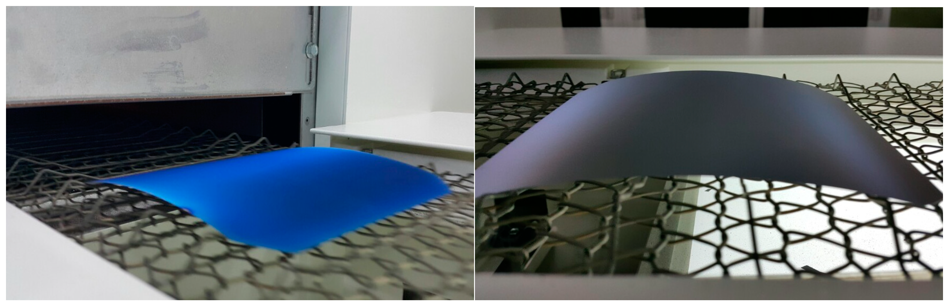
2.1. Bowing characteristics of thin c-Si solar cells
2.2. Theoretical analysis of bowing phenomenon of c-Si solar cells
3. Experiment Methods and Conditions
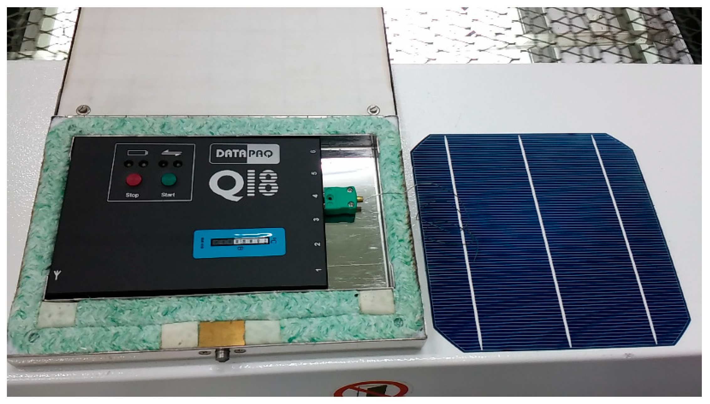
3.1. Experimental Conditions
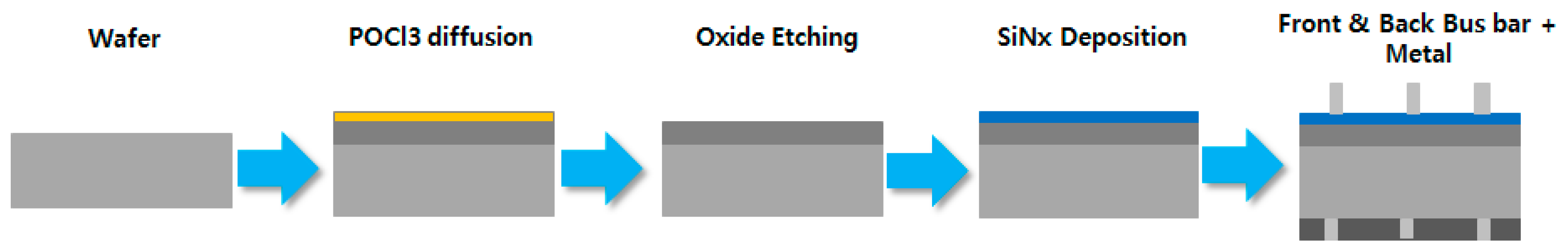
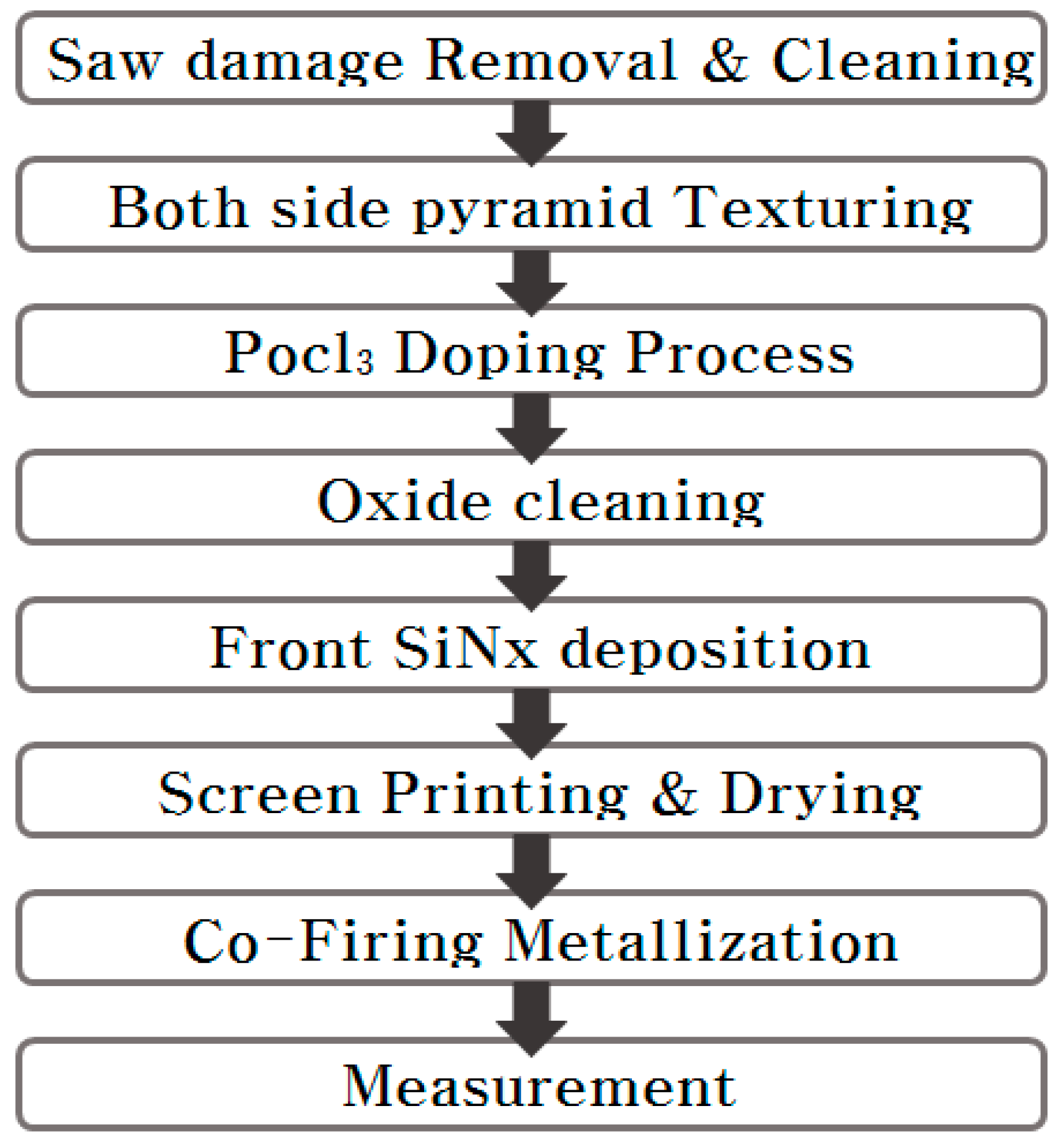
3.2. Partial Solar Cell Fabrication Process According to the c-Si Wafer Thickness
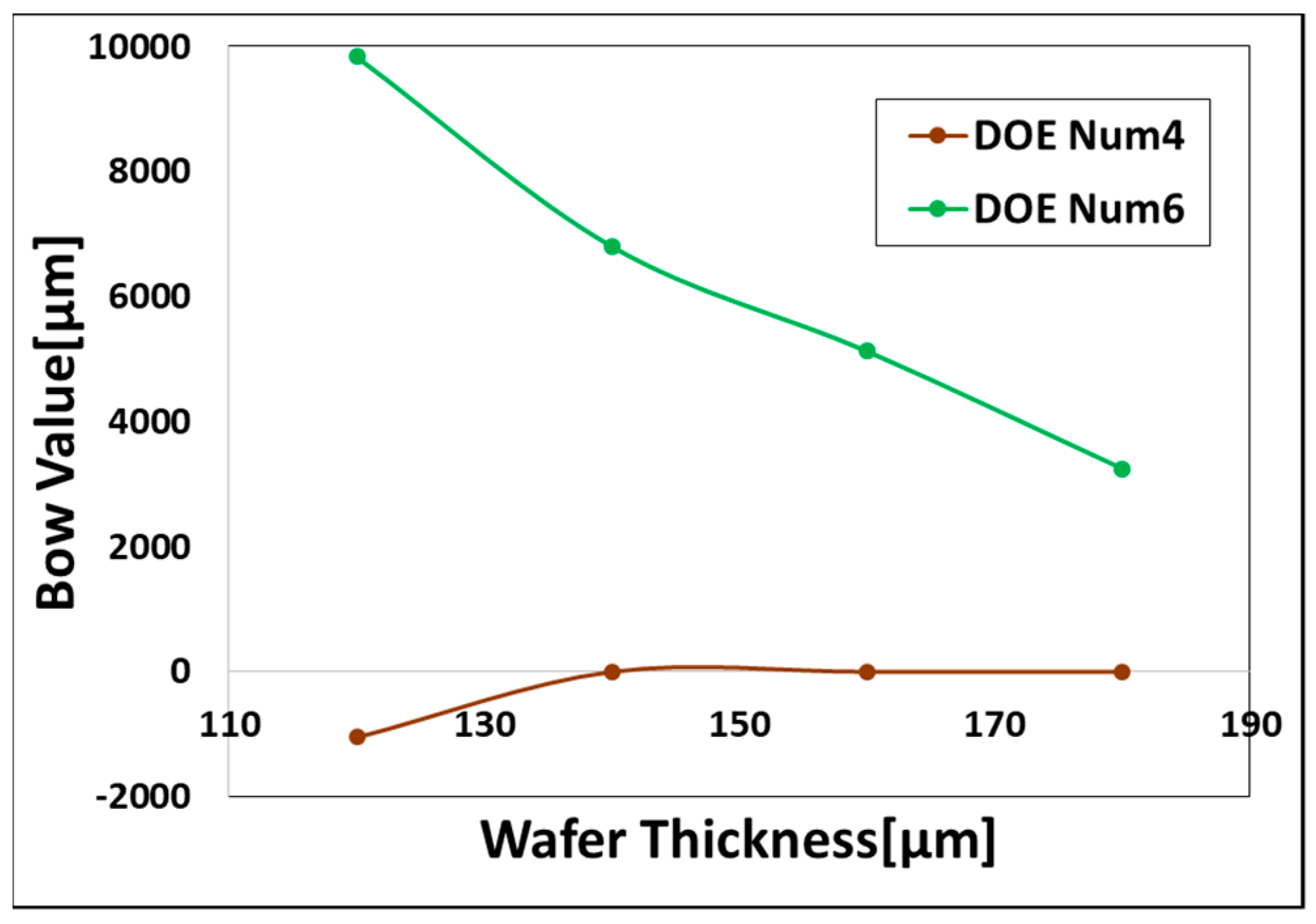
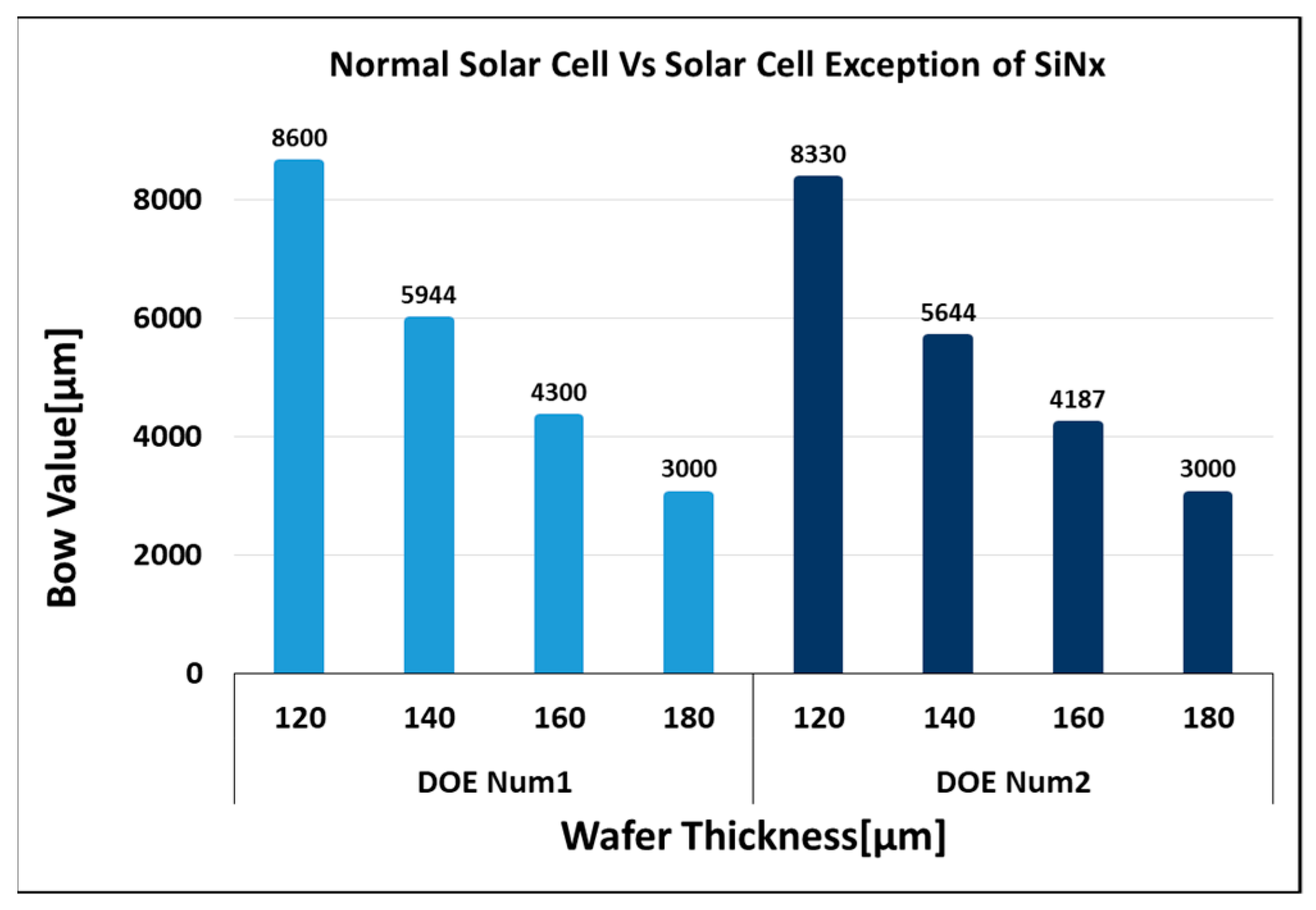
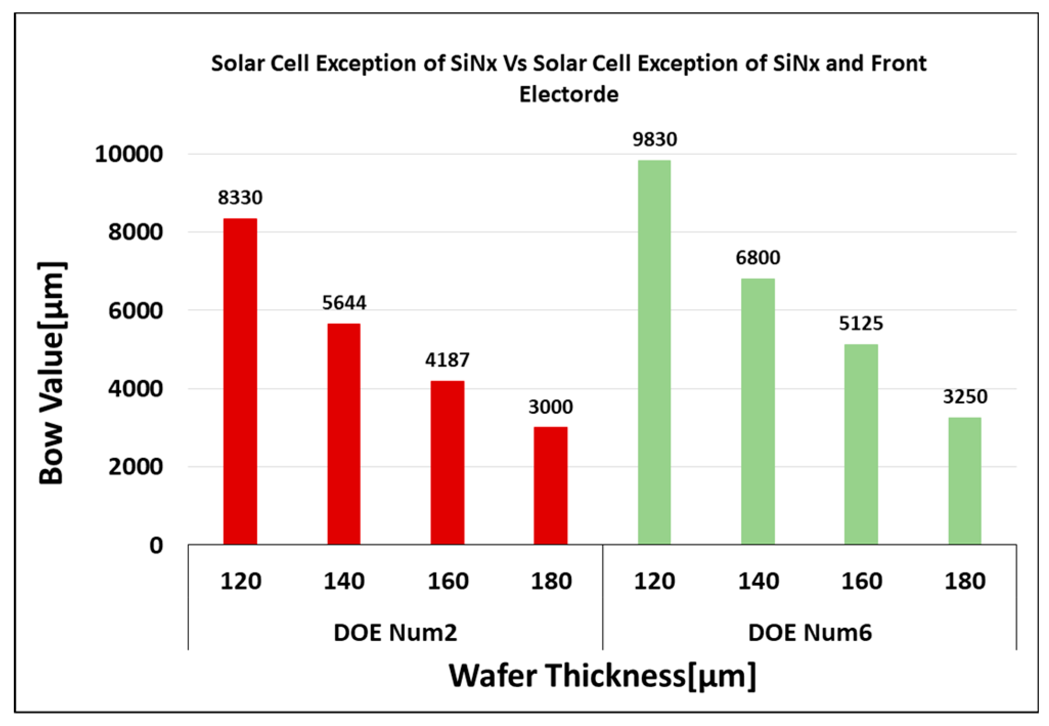
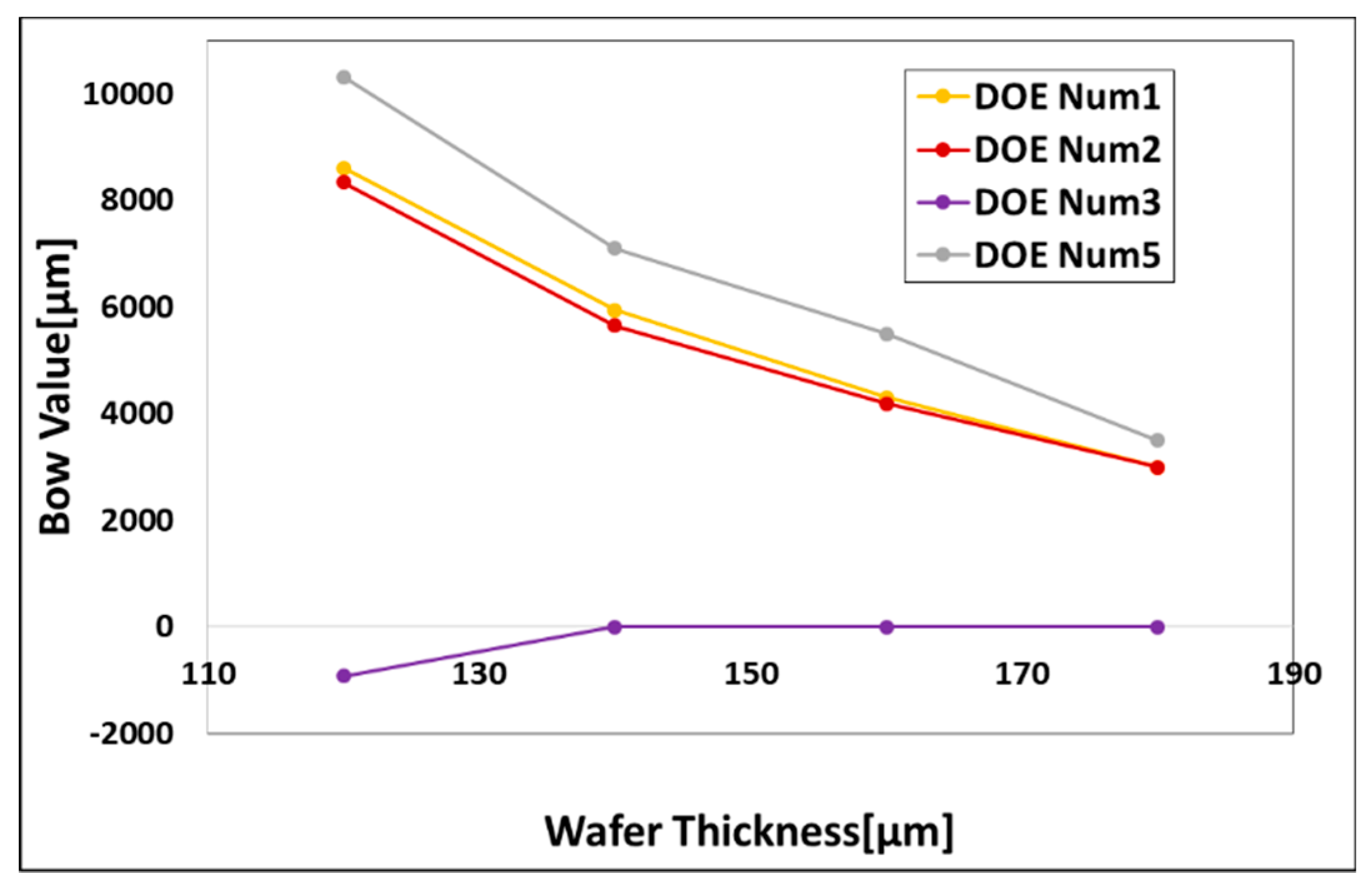
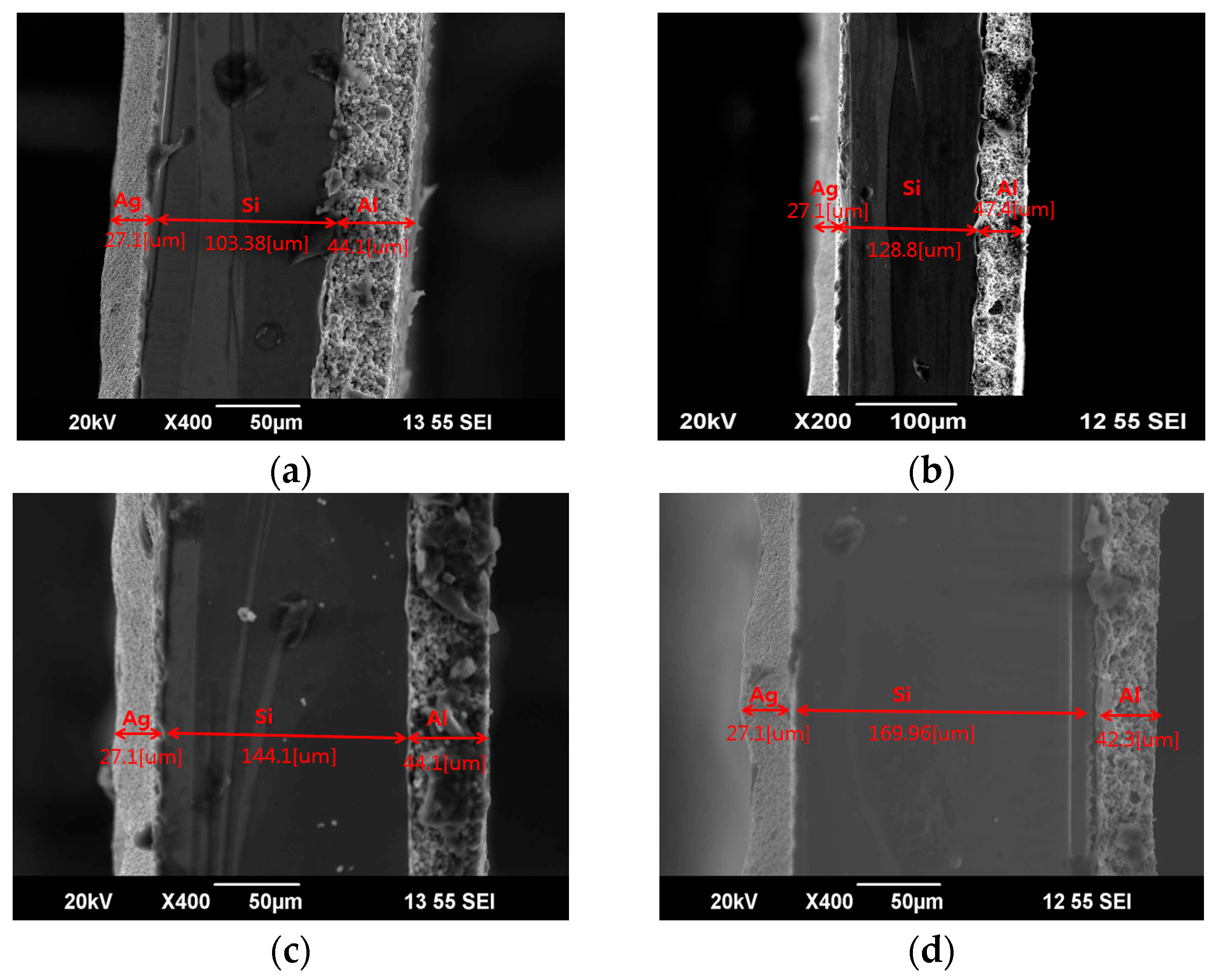
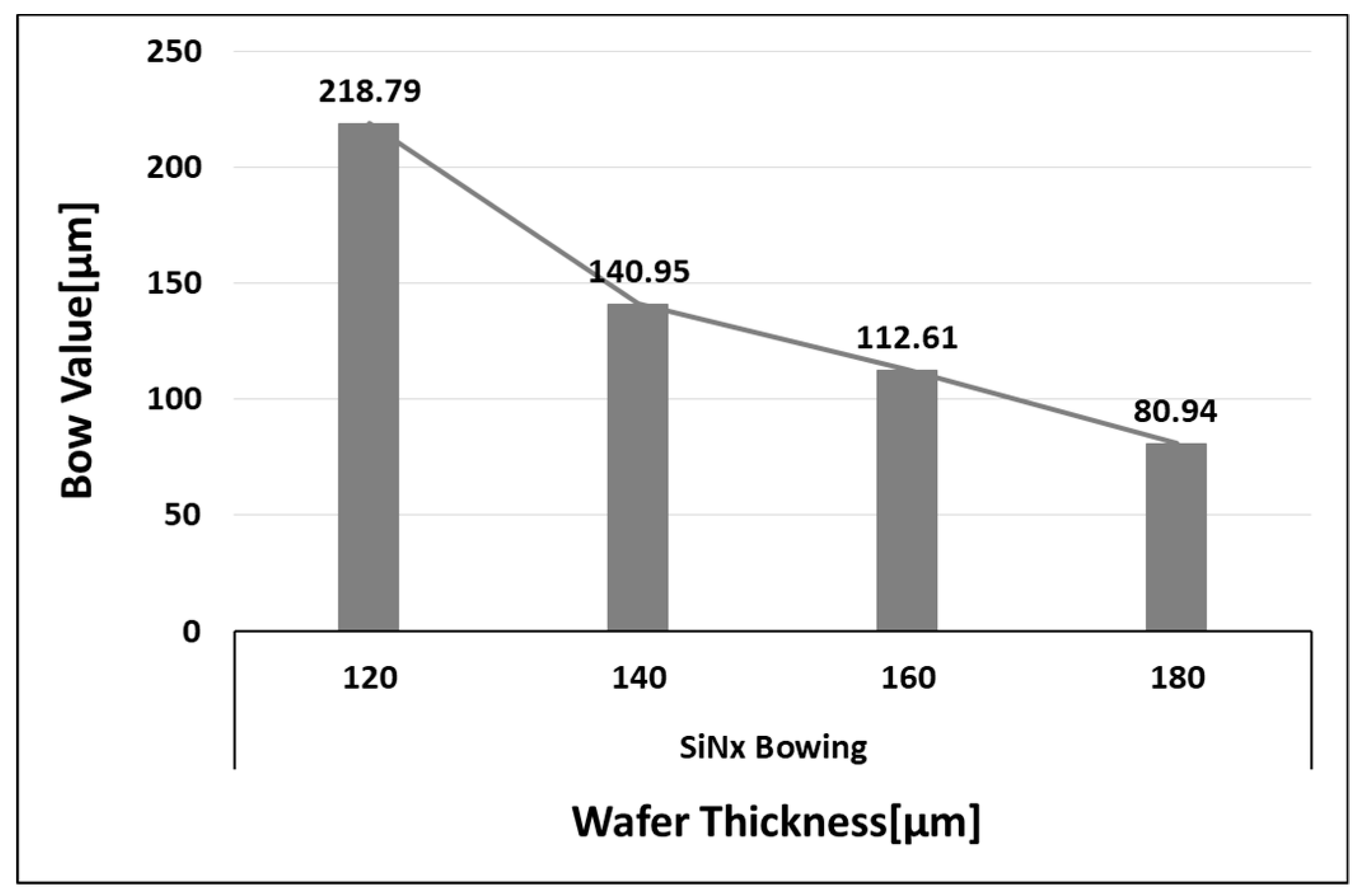
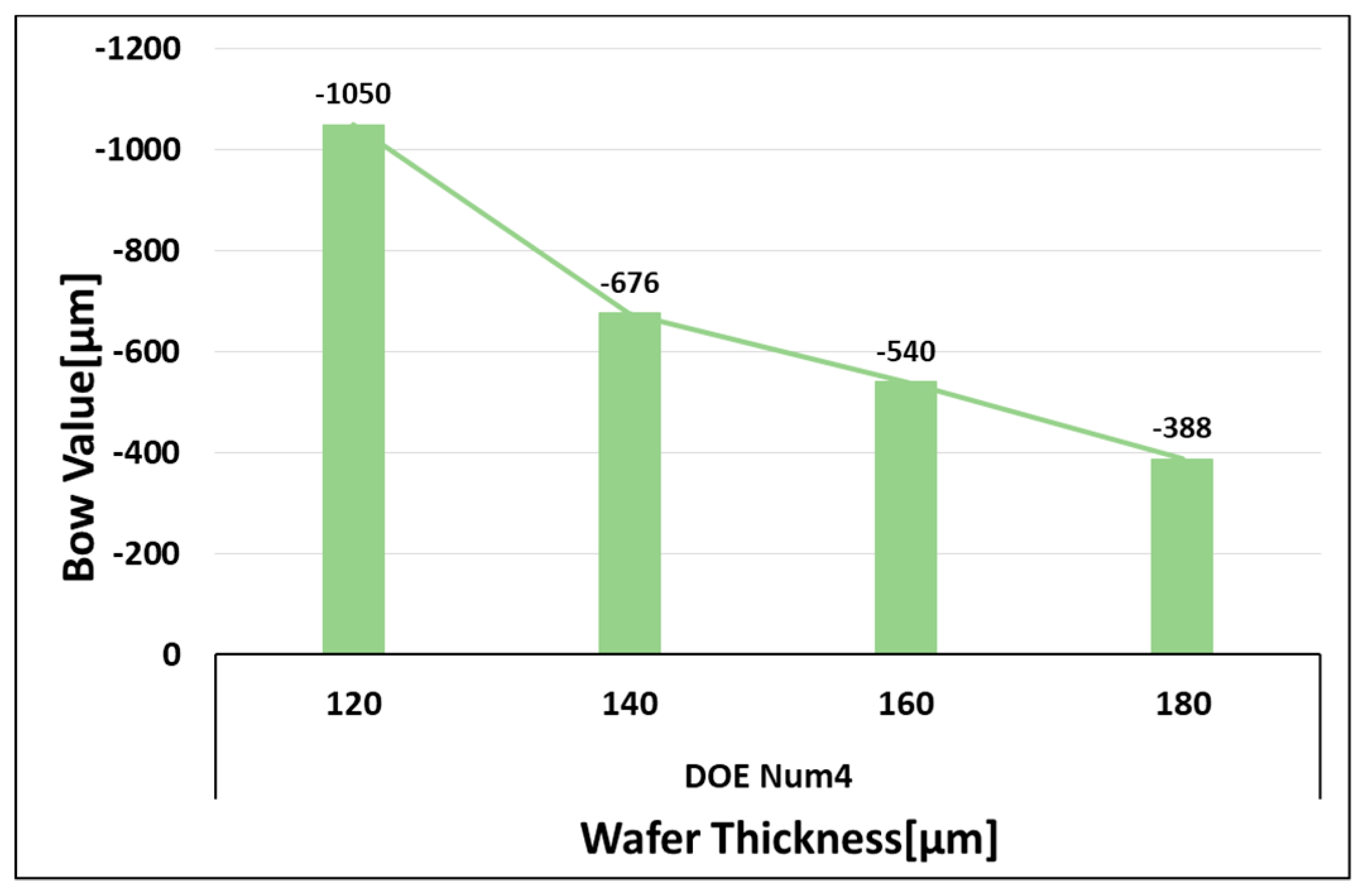
4. Results and Analysis
5. Conclusions
Author Contributions
Funding
Acknowledgments
Conflicts of Interest
References
- Demant, M.; Rein, S.; Krisch, J.; Schoenfelder, S.; Fischer, C.; Bartsch, S.; Preu, R. Detection and analysis of micro-cracks in multi crystalline silicon wafers during solar cell production. In Proceedings of the 2011 37th IEEE Photovoltaic Specialists Conference, Seattle, WA, USA, 19–24 June 2011; pp. 1641–1646. [Google Scholar]
- Metz, A.; Fischer, M.; Trube, J. International Technology Roadmap for Photovoltaic 2018, 8th ed.; 2017. Available online: http://www.etip-pv.eu/fileadmin/Documents/ETIP_PV_Conference_2017_Presentations/Session_II._1._Axel_Metz.pdf (accessed on 23 April 2019).
- Pietzer, T.M.; van Molken, J.I.; Ribland, S.; Breitenstein, O. Influence of cracks on the local current–voltage parameters of silicon solar cells. Prog. Photovolt. 2015, 23, 428–436. [Google Scholar] [CrossRef]
- Meyer, E.L.; van Dyk, E.E. Assessing the Reliability and Degradation of Photovoltaic Module Performance Parameters. IEEE Trans. Reliab. 2004, 53, 83–92. [Google Scholar] [CrossRef]
- Kaushika, N.D.; Rai, A.K. An investigation of mismatch losses in solar photovoltaic cell networks. Energy 2007, 32, 755–759. [Google Scholar] [CrossRef]
- Chen, C.H.; Lin, F.M.; Hu, H.T.; Yeh, F.Y. Residual stress and bow analysis for silicon solar cell Induced by soldering. In Proceedings of the International Symposium on Solar Cell Technologies, Taipei, Taiwan, 4–6 December 2008; Available online: http://140.116.36.16/paper/c37.pdf (accessed on 23 April 2019).
- Lai, C.M.; Su, C.H.; Lin, K.M. Analysis of the thermal stress and warpage induced by soldering in monocrystalline silicon cells bowing. Appl. Therm. Eng. 2013, 55, 7–16. [Google Scholar] [CrossRef]
- van Amstel, T.; Popovich, V.; Bennett, I.J. A Multiscale model of the Aluminium Layer at The Rear side of a Solar cell. In Proceedings of the 24th European Photovoltaic Solar Energy Conference and Exhibition, Hamburg, Germany, 21–25 September 2009. [Google Scholar]
- Yoon, P.; Joo, K.; Baek, T.; Song, H.; Chung, H.S.; Shin, S. Measurement of Bow in Silicon Solar Cell Using 3D Image Scanner. Korean Soc. Mech. Eng. 2012, 11, 1738–1739. [Google Scholar]
- Tae-Hyeon, B.; Ji-Hwa, H.; Kee-Joe, L.; Gi-Hwan, K.; Min-Gu, K.; Hee-Eun, S. Bow reduction in thin crystalline silicon solar cell with control of rear aluminum layer thickness. J. Korean Sol. Energy Soc. 2012, 32, 194–198. [Google Scholar]
- Mader, C.; Eitner, U.; Kajari-Schrder, S.; Brendel, R. Bow of Silicon Wafers After In-Line High-Rate evaporation of Aluminum. IEEE J. Photovolt. 2013, 3, 212–216. [Google Scholar] [CrossRef]
- Hilali, M.M.; Gee, J.M.; Hacke, P. Bow in screen printed back contact industrial silicon solar cells. Sol. Energy Mater. Sol. Cells 2007, 91, 1228–1233. [Google Scholar] [CrossRef]
- Kim, S.; Sridharan, S.; Khaditkar, C.; Shaikh, A. Aluminum pastes(lead-free/flow-bow) for Thin Wafers. In Proceedings of the Conference Record of the Thirty-first IEEE Photovoltaic Specialists Conference, Lake Buena Vista, FL, USA, 3–7 January 2005; pp. 1100–1102. [Google Scholar]
- Coulter, W.H.; Czyzewicz, R.C.; Farneth, W.E.; Prince, A.; Rajendran, R.G. Using Finite Element Methods and 3D Image Correlation to Model Solar Cell Bowing. In Proceedings of the Photovoltaic Specialists Conference (PVSC), Philadelphia, PA, USA, 7–12 June 2009; pp. 160–267. [Google Scholar]
- Bähr, M.; Dauwe, S.; Lawerenz, A.; Mittelstädt, L. Comparison of bow-avoiding Al-pastes for thin, large-area crystalline silicon solar cells. In Proceedings of the 20th Photovoltaic Solar Energy Conference, Barcelona, Spain, 6–10 June 2005. [Google Scholar]
- Schneider, A.; Gerhards, C.; Fath, P.; Bucher, E. Bow Reducing Factors for Thin Screen Printed Mc-Si Solar cells with Al BSF. In Proceedings of the Conference Record of the Twenty-Ninth IEEE Photovoltaic Specialists Conference, New Orleans, LA, USA, 19–24 May 2002; pp. 336–339. [Google Scholar]
- Frank, H. Aluminum-back surface field: Bow investigation and elimination. In Proceedings of the 20th European Photovoltaic Solar Energy Conference and Exhibition, Barcelona, Spain, 6–10 June 2005. [Google Scholar]
- van Silfhout, R.B.R.; van Driel, W.D.; Liz, Y.; Zhang, G.Q.; Emst, L.J. Prediction of Back-End Process induced wafer warpage and Experimental Verifican. In Proceedings of the Electronic Components and Technology Conference, San Diego, CA, USA, 28–31 May 2002; pp. 1182–1187. [Google Scholar]
- Lim, J.; Ham, S.; Jeong, B. Warpage modeling and characterization to simulate the fabrication process of wafer-level adhesive bonding. In Proceedings of the Electronic Manufacturing Technology Symposium, San Jose, CA, USA, 3–5 October 2007. [Google Scholar]
- Schwarzer, N.; Richter, F. On the determination of film stress from substrate bending: STONEY´ s formula and its limits. 2006. Available online: https://monarch.qucosa.de/api/qucosa%3A18453/attachment/ATT-0/ (accessed on 23 April 2019).
- Gerald, S.G. The tension of metallic films deposited by electrolysis. Proc. R. Soc. A 1909, 82, 172–175. [Google Scholar]
- Kim, S.; Lim, J.; Min, Y.; Ahn, H. Warpage behavior of thin solder cell package. In Proceedings of the 22nd Korean Confernce on Semiconductors (KCS), Incheon, Korea, 10–12 February 2015; p. 58. [Google Scholar]


| c-Si Wafer Thickness | Num | ARC | Front Side Electrode | Back Side Electrode |
|---|---|---|---|---|
| 120 μm, 140 μm, 160 μm, 180 μm | 1 | o | o | o |
| 2 | x | o | o | |
| 3 | o | o | x | |
| 4 | x | o | x | |
| 5 | o | x | o | |
| 6 | x | x | o |
© 2019 by the authors. Licensee MDPI, Basel, Switzerland. This article is an open access article distributed under the terms and conditions of the Creative Commons Attribution (CC BY) license (http://creativecommons.org/licenses/by/4.0/).
Share and Cite
Lim, J.R.; Kim, S.; Ahn, H.-K.; Song, H.-E.; Kang, G.H. Analysis of the Bowing Phenomenon for Thin c-Si Solar Cells using Partially Processed c-Si Solar Cells. Energies 2019, 12, 1593. https://doi.org/10.3390/en12091593
Lim JR, Kim S, Ahn H-K, Song H-E, Kang GH. Analysis of the Bowing Phenomenon for Thin c-Si Solar Cells using Partially Processed c-Si Solar Cells. Energies. 2019; 12(9):1593. https://doi.org/10.3390/en12091593
Chicago/Turabian StyleLim, Jong Rok, Sihan Kim, Hyung-Keun Ahn, Hee-Eun Song, and Gi Hwan Kang. 2019. "Analysis of the Bowing Phenomenon for Thin c-Si Solar Cells using Partially Processed c-Si Solar Cells" Energies 12, no. 9: 1593. https://doi.org/10.3390/en12091593
APA StyleLim, J. R., Kim, S., Ahn, H.-K., Song, H.-E., & Kang, G. H. (2019). Analysis of the Bowing Phenomenon for Thin c-Si Solar Cells using Partially Processed c-Si Solar Cells. Energies, 12(9), 1593. https://doi.org/10.3390/en12091593