High-Efficiency DC–DC Converter with Charge-Recycling Gate-Voltage Swing Control

Abstract
:1. Introduction
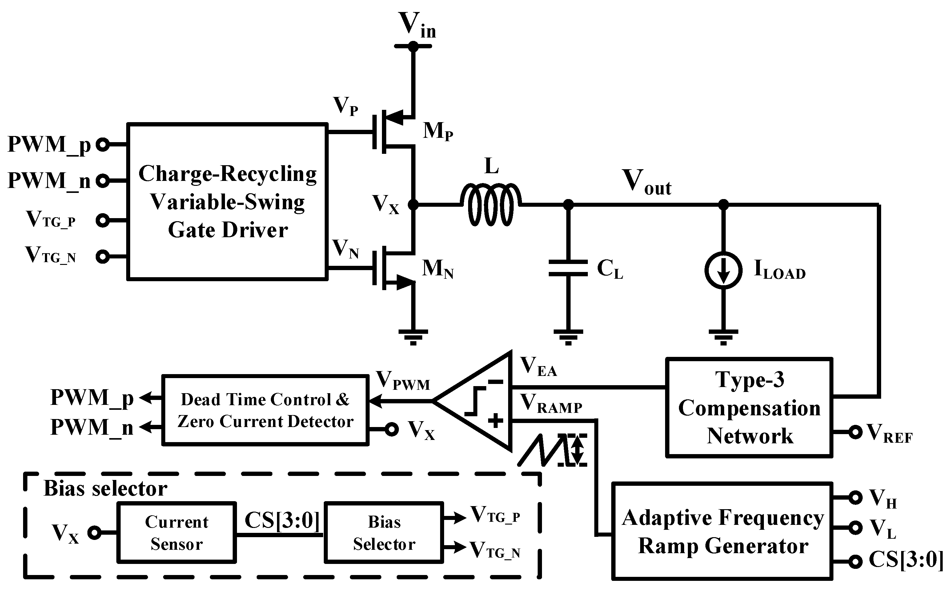
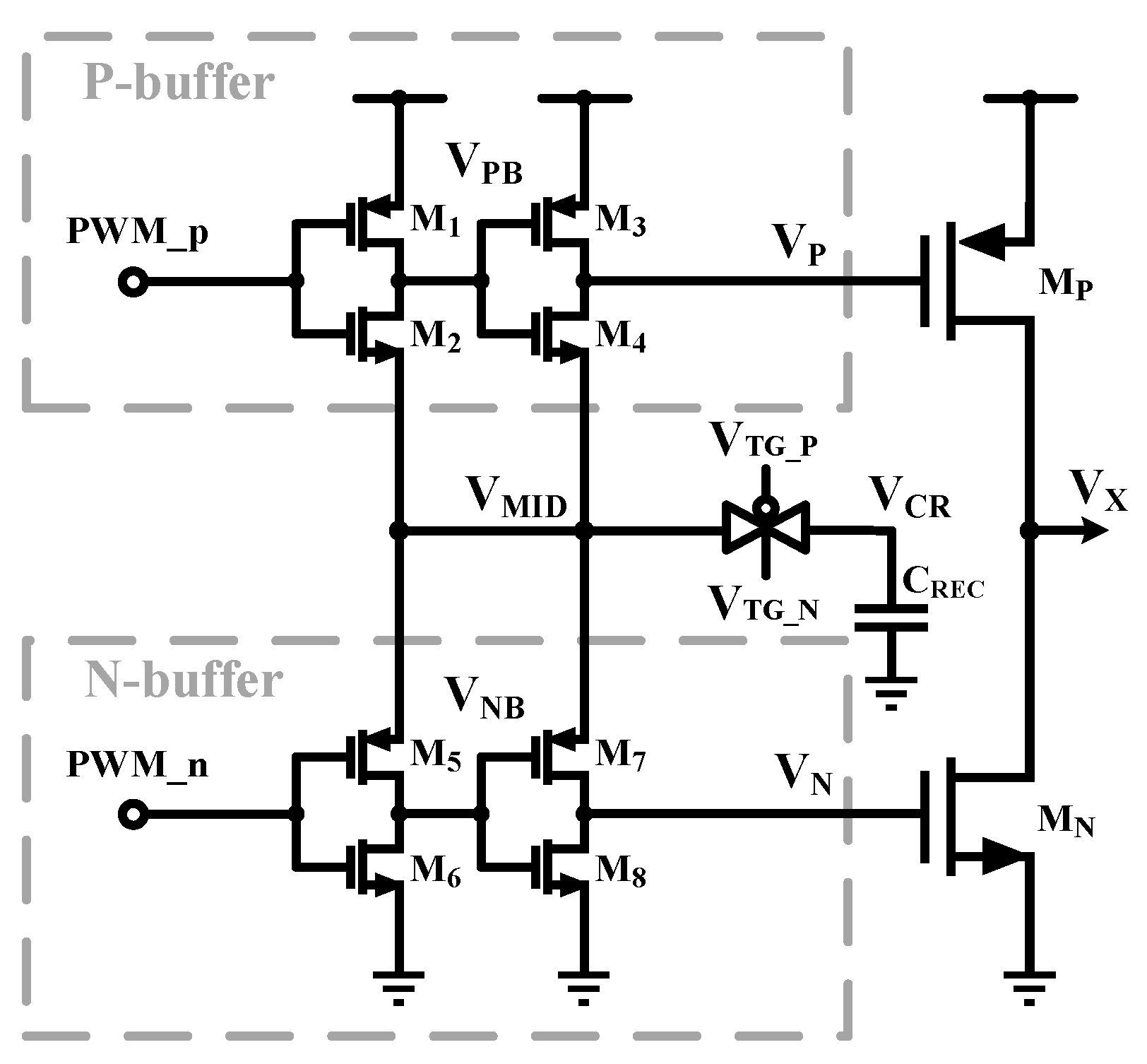
2. Proposed Buck Converter
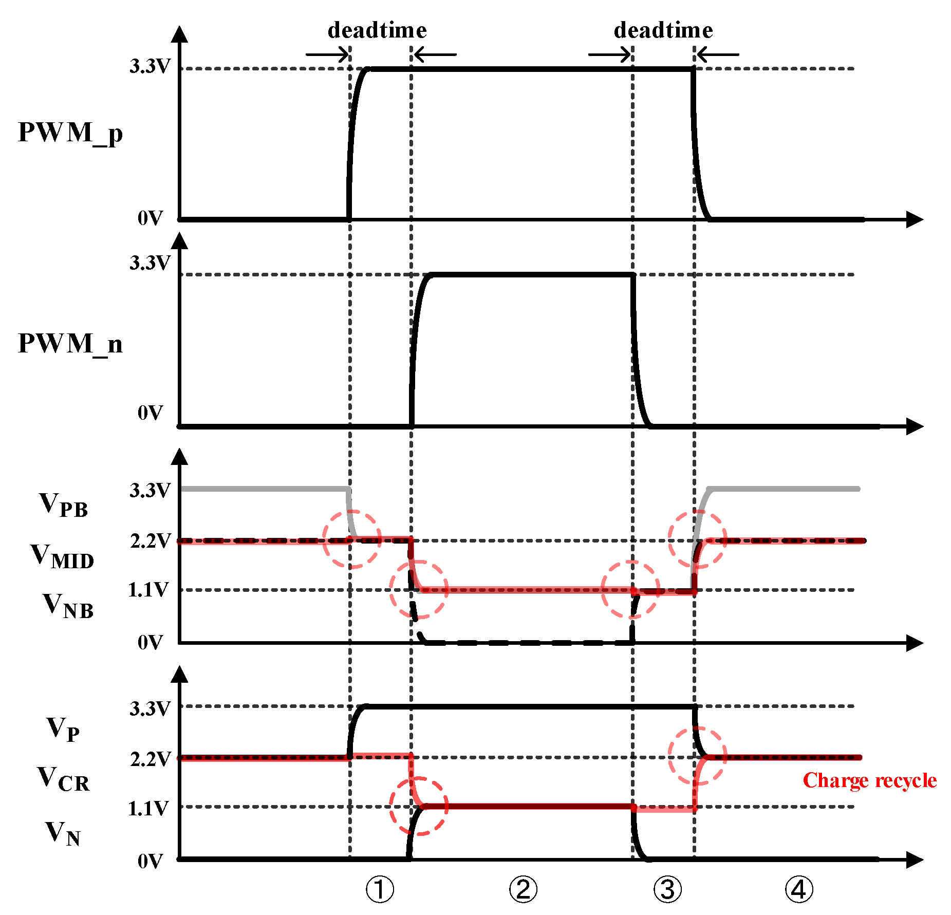
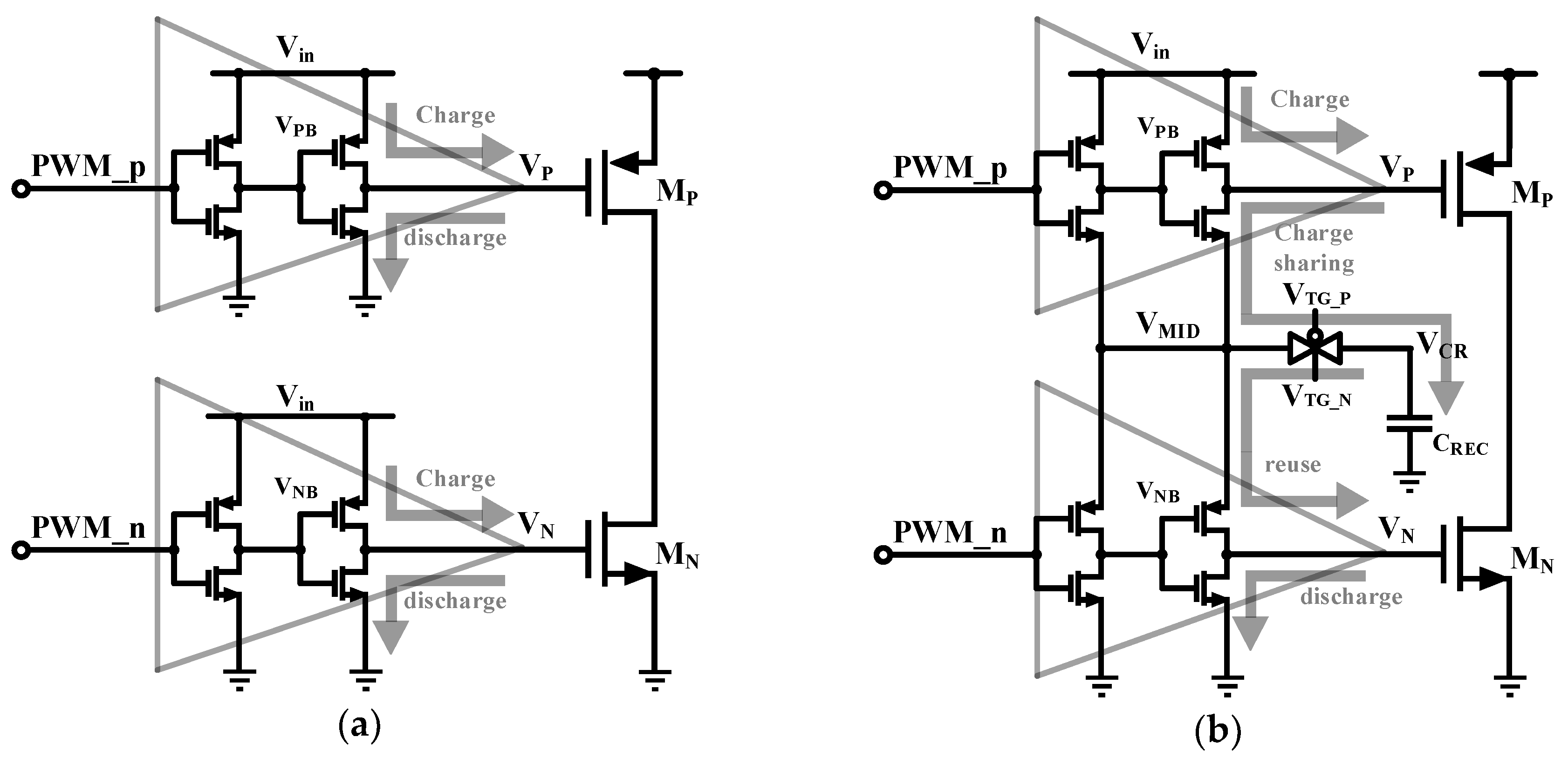
2.1. Charge-Recycling Gate Driving
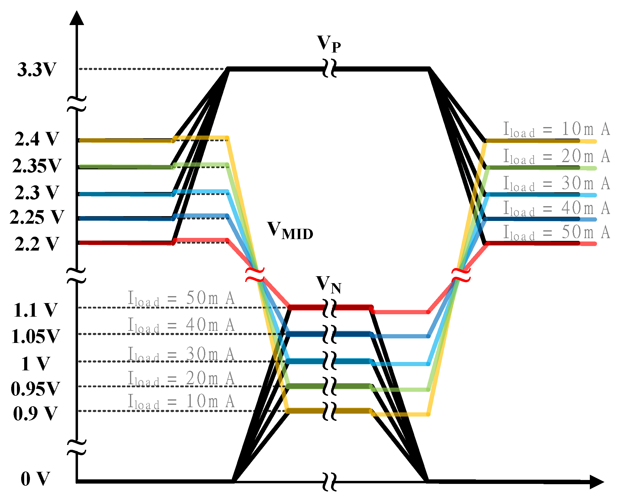
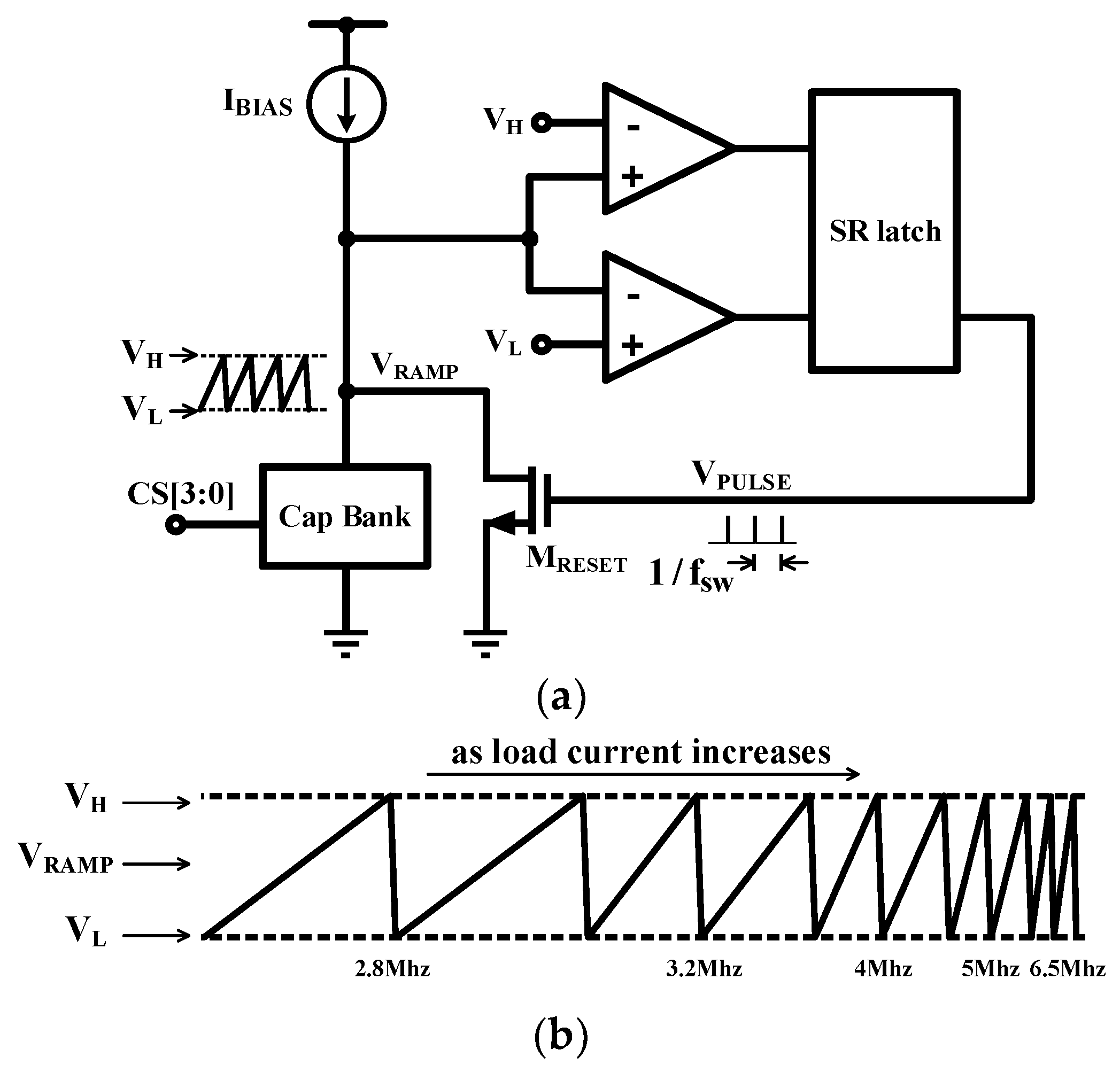
2.2. Variable Gate-Voltage Swing Control
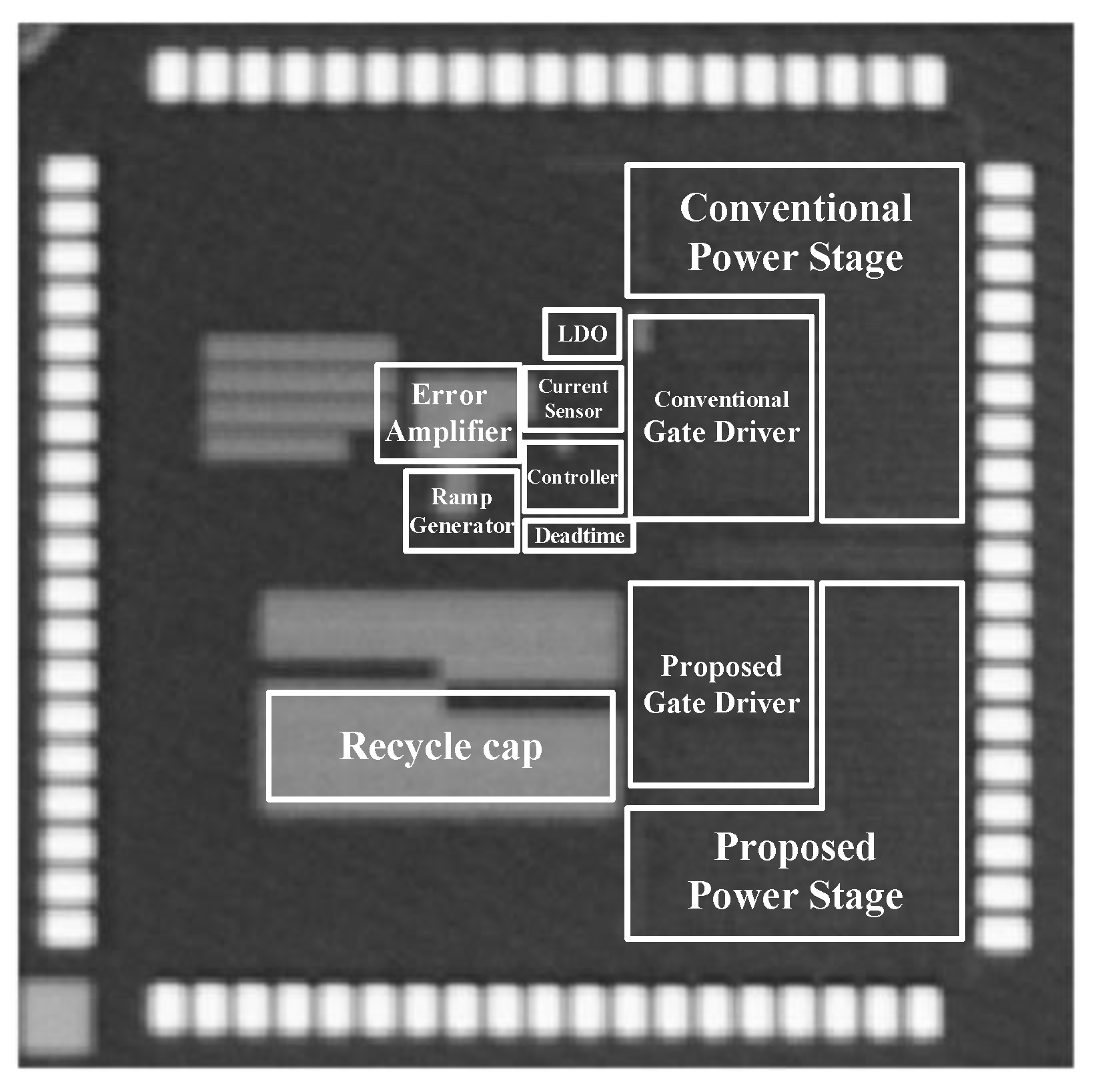
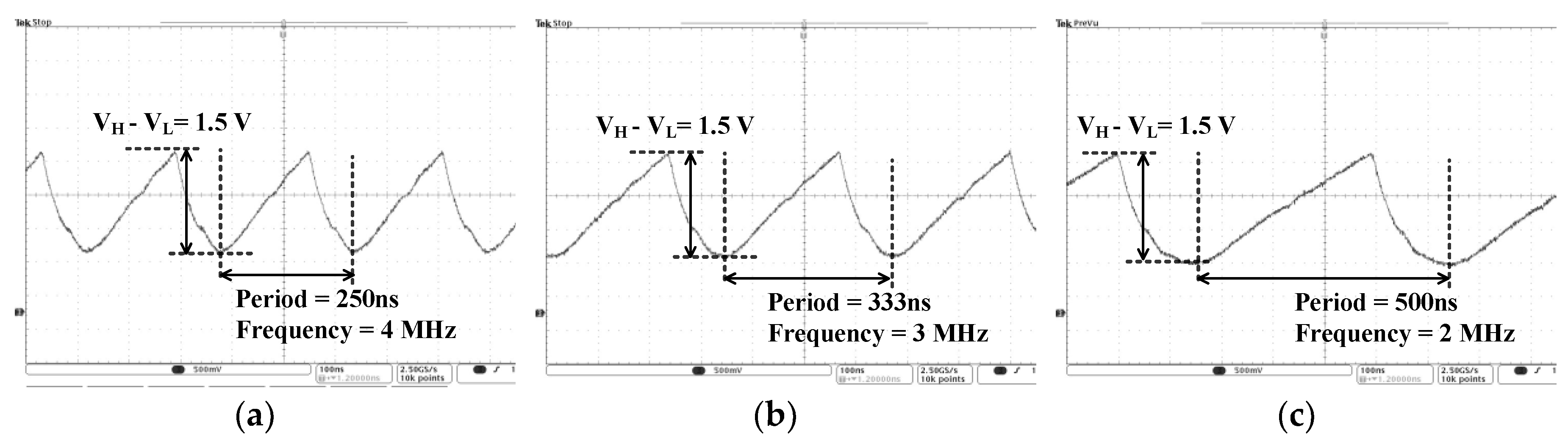
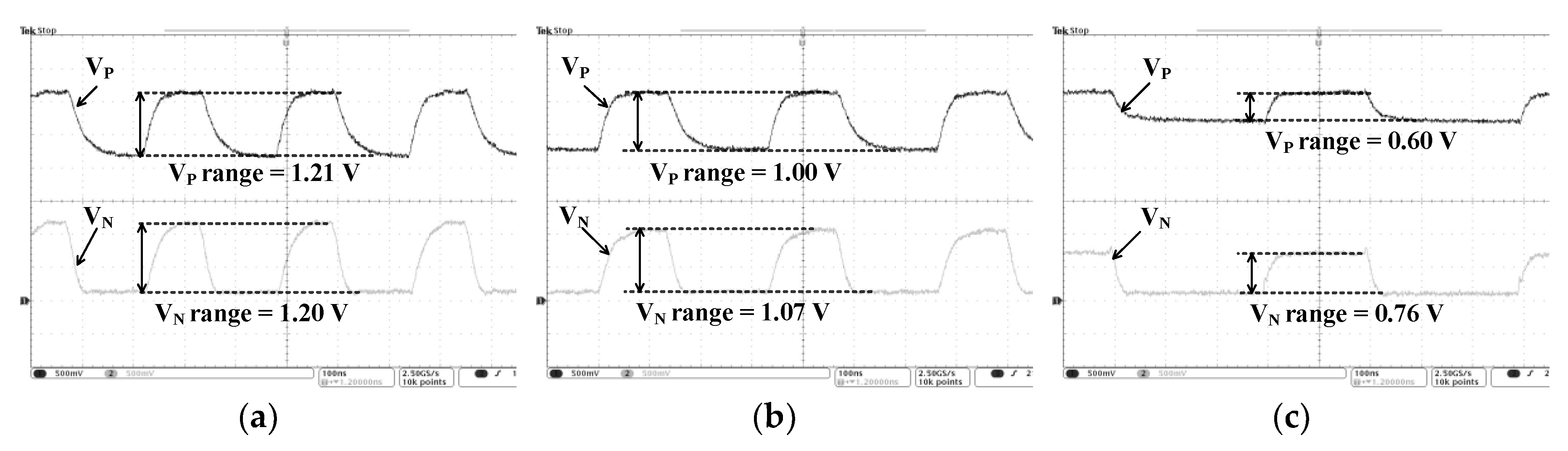
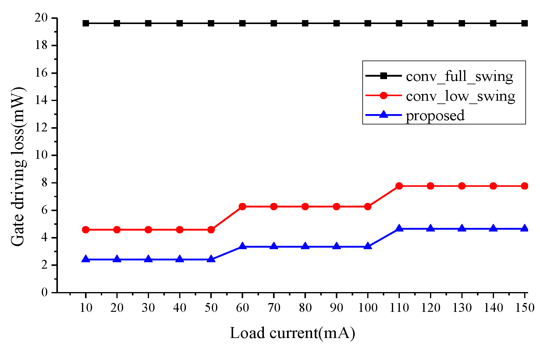
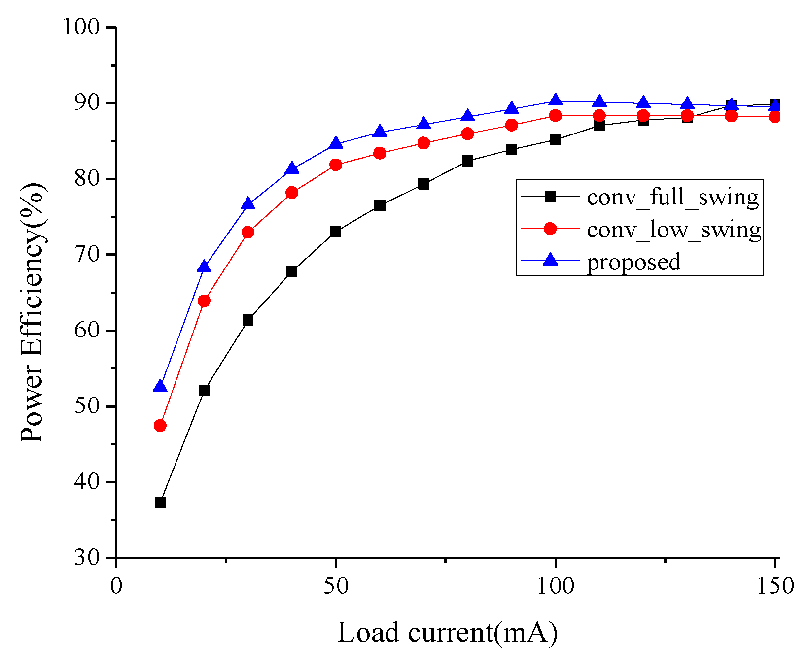
3. Measurement Results
4. Conclusions
Author Contributions
Funding
Conflicts of Interest
References
- Ogawa, T.; Hatanaka, S.; Taniguchi, K. An on-chip high-efficiency dc–dc converter with a compact timing edge control circuit. In Proceedings of the 2002 Symposium on VLSI Circuits. Digest of Technical Papers (Cat. No.02CH37302), Honolulu, HI, USA, 13–15 June 2002; pp. 278–279. [Google Scholar] [CrossRef]
- Mulligan, M.D.; Broach, B.; Lee, T.H. A constant-frequency method for improving light-load efficiency in synchronous buck converters. IEEE Power Electron. Lett. 2005, 3, 24–29. [Google Scholar] [CrossRef]
- Duan, X.; Huang, A. Current-mode variable-frequency control architecture for high-current low-voltage dc-dc converters. IEEE Trans. Power Electron. 2006, 21, 1133–1137. [Google Scholar] [CrossRef]
- Liu, P.J.; Yeh, W.S.; Tai, J.N.; Chen, H.-S.; Chen, J.H.; Chen, Y.J. A High-Efficiency CMOS DC-DC Converter with 9-μs Transient Recovery Time. IEEE Trans. Circuits Syst. I 2012, 59, 575–583. [Google Scholar] [CrossRef]
- Liou, W.R.; Yeh, M.L.; Kuo, Y.L. A High Efficiency Dual-Mode Buck Converter IC For Portable Applications. IEEE Trans. Power Electron. 2008, 23, 667–677. [Google Scholar] [CrossRef]
- Wu, H.H.; Wei, C.L.; Hsu, Y.C.; Darling, R.B. Adaptive Peak-Inductor-Current-Controlled PFM Boost Converter with a Near-Threshold Startup Voltage and High Efficiency. IEEE Trans. Power Electron. 2015, 30, 1956–1964. [Google Scholar] [CrossRef]
- Kim, S.-J.; Cho, W.-S.; Robert, P.-P.; Pavan, K.-H. A 10 MHz 2 mA-800 mA 0.5 V–1.5 V 90% peak efficiency time-based buck converter with seamless transition between PWM/PFM modes. IEEE J. Solid-State Circuits 2018, 53, 814–824. [Google Scholar] [CrossRef]
- Chen, H.M.; Huang, H.C.; Jheng, S.H.; Huang, H.T.; Huang, Y.S. High-Efficiency PFM Boost Converter with an Accurate Zero Current Detector. IEEE Trans. Circuits Syst. II 2018, 65, 1644–1648. [Google Scholar] [CrossRef]
- Huang, H.W.; Chen, K.H.; Kuo, S.Y. Dithering skip modulation, width and dead time controllers in highly efficient DC-DC converters for system-on-chip applications. IEEE J. Solid-State Circuits 2007, 42, 2451–2465. [Google Scholar] [CrossRef]
- Tsai, J.C.; Huang, T.Y.; Lai, W.W.; Chen, K.H. Dual modulation technique for high efficiency in high switching buck converters over a wide load range. In Proceedings of the 2010 IEEE International Symposium on Circuits and Systems, Paris, France, 30 May–2 June 2010; pp. 3709–3712. [Google Scholar] [CrossRef]
- Musunuri, S.; Chapman, P. Improvement of light-load efficiency using width-switching scheme for CMOS transistors. IEEE Power Electron. Lett. 2005, 3, 105–110. [Google Scholar] [CrossRef]
- Kursun, V.; Narendra, S.G.; De, V.K.; Friedman, E.G. Low-voltage-swing monolithic dc-dc conversion. IEEE Trans. Circuits Syst. II Express Briefs 2004, 51, 241–248. [Google Scholar] [CrossRef]
- Sun, Z.; Chew, K.-W.-R.; Tang, H.; Siek, L. Adaptive Gate Switching Control for Discontinuous Conduction Mode DC–DC Converter. IEEE Trans. Power Electron. 2014, 29, 1311–1320. [Google Scholar] [CrossRef]
- Trescases, O.; Yue, W. A survey of light-load efficiency improvement techniques for low-power DC-DC converters. In Proceedings of the 8th International Conference on Power Electronics—ECCE Asia, Jeju, South Korea, 30 May–3 June 2011; pp. 326–333. [Google Scholar] [CrossRef]
- Mulligan, M.; Broach, B.; Lee, T. A 3 MHz low-voltage buck converter with improved light load efficiency. In Proceedings of the 2007 IEEE International Solid-State Circuits Conference, Digest of Technical Papers. San Francisco, CA, USA, 11–15 February 2007; pp. 528–620. [Google Scholar] [CrossRef]
- Alimadadi, M.; Sheikhaei, S.; Lemieux, G.; Mirabbasi, S.; Dunford, W.; Palmer, P. A fully integrated 660 MHz low-swing energy-recycling dc dc converter. IEEE Trans. Power Electron. 2009, 24, 1475–1485. [Google Scholar] [CrossRef]
- Wen, Y.; Trescases, O. Closed-loop control of gate-charge recycling in a 20 MHz dc-dc converter. In Proceedings of the IEEE 12th Workshop on Control and Modeling for Power Electronics (COMPEL), Boulder, CO, USA, 28–30 June 2010; pp. 1–7. [Google Scholar] [CrossRef]
- Abdulslam, A.; Mohammad, B.; Ismail, M.; Mercier, P.; Ismail, Y. A 93% Peak Efficiency Fully-Integrated Multilevel Multistate Hybrid DC–DC Converter. IEEE Trans. Circuits Syst. I 2018, 65, 2617–2630. [Google Scholar] [CrossRef]


| [4] | [5] | [6] | [8] | [13] | [15] | [16] | [18] | This Work | |
|---|---|---|---|---|---|---|---|---|---|
| Technology (nm) | 350 | 350 | 180 | 180 | 180 | 500 | 180 | 65 | 65 |
| Supply voltage (V) | 2.6–3.6 | 2.7–5 | 0.22–1.3 | 1.2 | 0.9–1.4 | 3.6 | 2.2 | 1.2 | 3.3 |
| Output Voltage (V) | 0.6–2.1 | 1 | 1.8 | 1.8 | 2.5 | 1.8 | 0.75–1.0 | 0.1–1.1 | 1.2–2.3 |
| Inductor (µH) | 22 | 10 | 4.7 | 10 | 1 | 4.7 | 2.2 × 10⁻³ | 5.8 × 10⁻³ | 4.7 |
| Capacitor (µF) | 22 | 10 | N/A | 47 | 10 | 3.3 | 1.1 × 10⁻³ | 4.4 × 10⁻³ | 4.7 |
| Frequency (MHz) | 1 | 0.1–0.6 | 0.02–0.06 | 0.001–0.04 | 0.8 | 3 | 660 | 10–40 | 2–4 |
| Die area(mm2) | 3.04 | 3.57 | 0.72 | 0.43 | 1.5 | 5.3 | 2.5 | 2.34 | 1.3 |
| Load current (mA) | 450 | 460 | 50 | 50 | 60 | 500 | 40–55 | 100 | 1–700 |
| Max. efficiency (%) | 90 | 95 | 90.6 | 88.39 | 88 | 89.1 | 65 | 93.2 | 90.3 |
| Area/efficiency | 2.74 | 3.39 | 0.79 | 0.49 | 1.70 | 5.95 | 3.85 | 2.51 | 1.44 |
© 2019 by the authors. Licensee MDPI, Basel, Switzerland. This article is an open access article distributed under the terms and conditions of the Creative Commons Attribution (CC BY) license (http://creativecommons.org/licenses/by/4.0/).
Share and Cite
Suh, J.-D.; Yun, Y.-H.; Kong, B.-S. High-Efficiency DC–DC Converter with Charge-Recycling Gate-Voltage Swing Control. Energies 2019, 12, 899. https://doi.org/10.3390/en12050899
Suh J-D, Yun Y-H, Kong B-S. High-Efficiency DC–DC Converter with Charge-Recycling Gate-Voltage Swing Control. Energies. 2019; 12(5):899. https://doi.org/10.3390/en12050899
Chicago/Turabian StyleSuh, Jung-Duk, Yeong-Ho Yun, and Bai-Sun Kong. 2019. "High-Efficiency DC–DC Converter with Charge-Recycling Gate-Voltage Swing Control" Energies 12, no. 5: 899. https://doi.org/10.3390/en12050899
APA StyleSuh, J.-D., Yun, Y.-H., & Kong, B.-S. (2019). High-Efficiency DC–DC Converter with Charge-Recycling Gate-Voltage Swing Control. Energies, 12(5), 899. https://doi.org/10.3390/en12050899