Article

Resonant Converter with Soft Switching and Wide Voltage Operation

Department of Electrical Engineering, NYUST, Yunlin 640, Taiwan
Energies 2019, 12(18), 3479; https://doi.org/10.3390/en12183479
Submission received: 25 July 2019 / Revised: 4 September 2019 / Accepted: 8 September 2019 / Published: 9 September 2019

Abstract

:
A new DC/DC resonant converter with wide output voltage range operation is presented and studied to have the benefits of low switching losses on active devices and low voltage stresses on power diodes. To overcome serious reverse recovery losses of power diodes on a conventional full-bridge pulse-width modulation converter, the resonant converter is adopted to reduce the switching loss and increase the circuit efficiency. To extend the output voltage range in conventional half-bridge or full-bridge resonant converters, the secondary sides of two diode rectifiers are connected in series to have wide output voltage operation. The proposed converter can be either operated at one-resonant-converter mode for low voltage range or two-resonant-converter mode for high voltage range. Thus, the voltage rating of power diodes is decreased. Experiments with the design example are given to show the circuit performance and validate the theoretical discussion and analysis.

Graphical Abstract

1. Introduction

Power saving and power loss issues have become more and more important with respect to reducing the effect of global warming. Low power loss means less power demand is needed from the utility company. Modern power converters have demanded the development of high power density and low power loss for modern consumer and industry products. Soft switching techniques or wide-band gap power devices, such as SiC or GaN power switches, have been widely developed to lessen the switching losses. SiC and GaN have low switching loss characteristics and power converters and can operate at high frequency and high power density, however, the wide-band gap power switches are much more expensive than the conventional MOSFETs. For zero voltage switching techniques, a quasi-resonant (QR) approach has been applied in flyback [1,2] to lessen the switching loss. The circuit efficiency of QR flyback with synchronous rectifier can be higher than 90%. Active clamp techniques [3] have been applied in buck, boost, flyack, and forward converters to lessen the switching losses for low-power applications. More components are needed in the circuit, and these additional components introduce more power loss. For medium-power products, resonant converters [4,5,6,7] and full-bridge pulse width modulation converters [8,9,10,11] were developed to reduce switching losses. Full-bridge converters lose soft switching operation at low output power and the circuit efficiency will decrease at low load conditions. The resonant converters have soft switching characteristics on power semiconductors over the full load range so that the efficiency of the resonant converter at low load is better than phase-shift full-bridge converters. The limited voltage variation range is the main drawback of the resonant converters. If the voltage operation range is increased, then the low inductor ratio and low quality factor should be used. However, the circulating current and conduction loss on the primary side will increase and the circuit efficiency decreases.
Wide output voltage power converters are demanded for battery chargers for hybrid electric vehicles or outdoor LED lighting systems. In electric vehicle and hybrid electric vehicle battery charging systems, the single-phase power factor corrector and isolated DC converter are used in type I and II charging systems, and the three-phase power factor corrector and full-bridge DC converter are adopted in type III charging system. The output voltage of the high-voltage battery stack in PHEV and EV varies widely with battery capacity, such as 200–420 V. In outdoor LED lighting systems, the DC output voltage is variable for different series and parallel combinations of LED strings’ applications, such as 120–360 V. The DC-DC converters with wide output voltage variation have been developed for battery chargers. To achieve wide output voltage capability, the full-bridge DC converters with phase-shift pulse width modulation were presented and discussed in [12,13] to have high circuit efficiency and low switching losses. The voltage range is limited to less than 2:1 (vo,max = 2vo,min) or 3:1 (vo,max = 3vo,min) due to low converter efficiency in low duty cycle or low output voltage cases. To realize a wide output voltage range, the basic circuit topologies are two-stage DC-DC converters (boost or buck converter + full-bridge converter) to implement 4:1 (vo,max = 4vo,min) voltage variation. However, the circuit efficiency is reduced in these circuit topologies. The hybrid resonant converter with half-bridge or full-bridge operation has been studied in [14,15,16] to increase the voltage operation range, such as a 4:1 voltage range, vin,max = 4vin,min. The main problems are that a transient operation interval will be introduced between the half-bridge resonant circuit and the full-bridge resonant circuit operation, and one power switch is always conducting under the half-bridge resonant circuit to decrease circuit efficiency. The voltage rating of power diodes on conventional full-bridge or center-tapped diode rectifiers equals the output voltage or two times the output voltage, respectively. The rectifier diodes have serious voltage stress problems for high-voltage output conditions.
A hybrid resonant circuit with an input-parallel output-series structure is presented and studied to accomplish the improvements of the low-voltage rating on power diodes, wide voltage operation range, and wide soft switching range. By using the frequency modulation approach, the proposed converter is controlled under inductive impedance. The soft switching operation of power devices is achieved. The switching losses on power semiconductors are reduced. To overcome the high-voltage rating problem on rectifier diodes, two full-bridge diode rectifiers are employed on the proposed circuit. For high-voltage output, two full-bridge resonant converters are all operated and the secondary-side rectified voltages are series-connected. The voltage rating of each diode is Vo,H/2 instead of Vo,H in conventional DC-DC converters. On the other hand, only one full-bridge resonant converter is operated under the low-voltage output case. Only one diode rectifier is connected to the output load and the other diode rectifier is bypassed. The voltage rating of the power diodes is Vo,L. The drawback of the high-voltage rating on rectifier diodes is improved in the presented circuit. The theoretical analysis, the principle of operation, and the design procedure are provided in this paper. Finally, a 2 kW laboratory circuit was built and tested. Experimental results are used to confirm the theoretical analysis and demonstrate the helpfulness of the presented hybrid resonant converter for wide output voltage capability.

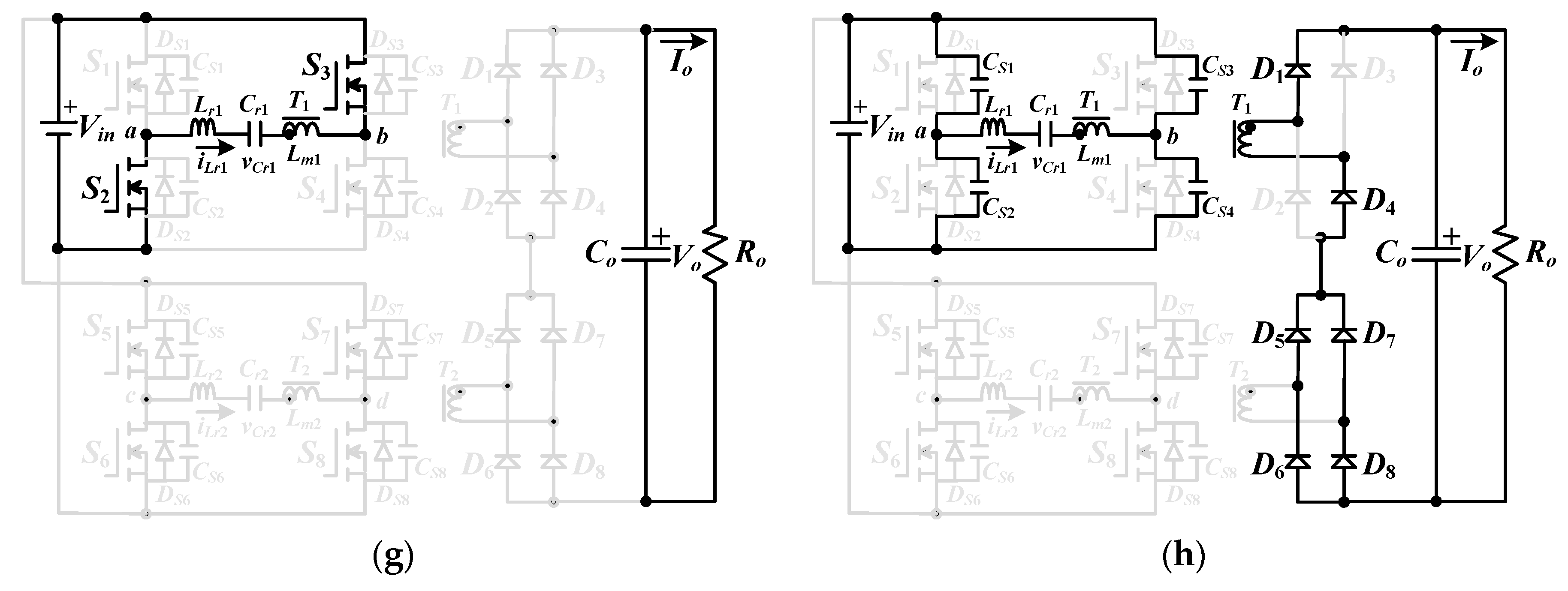
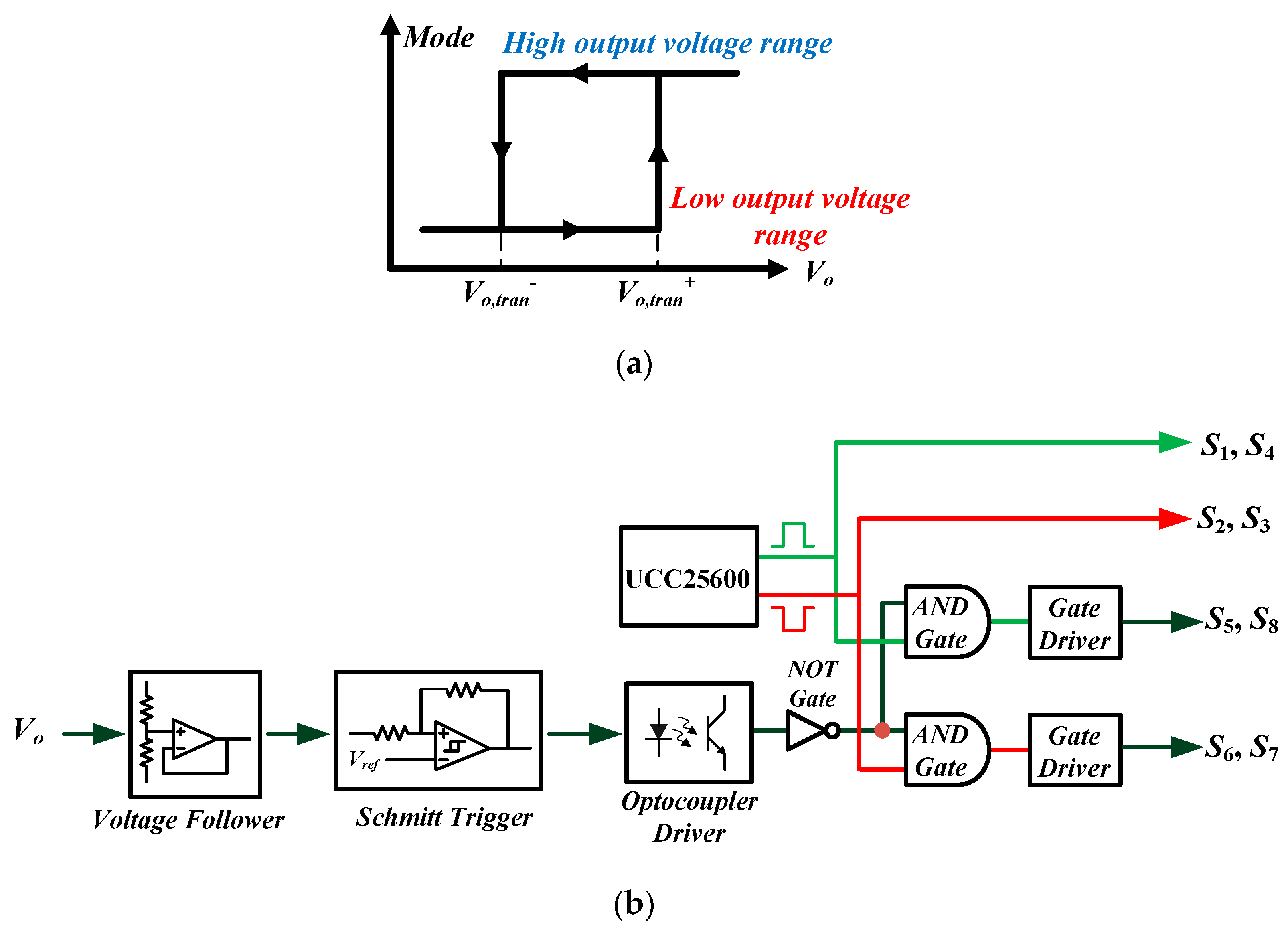
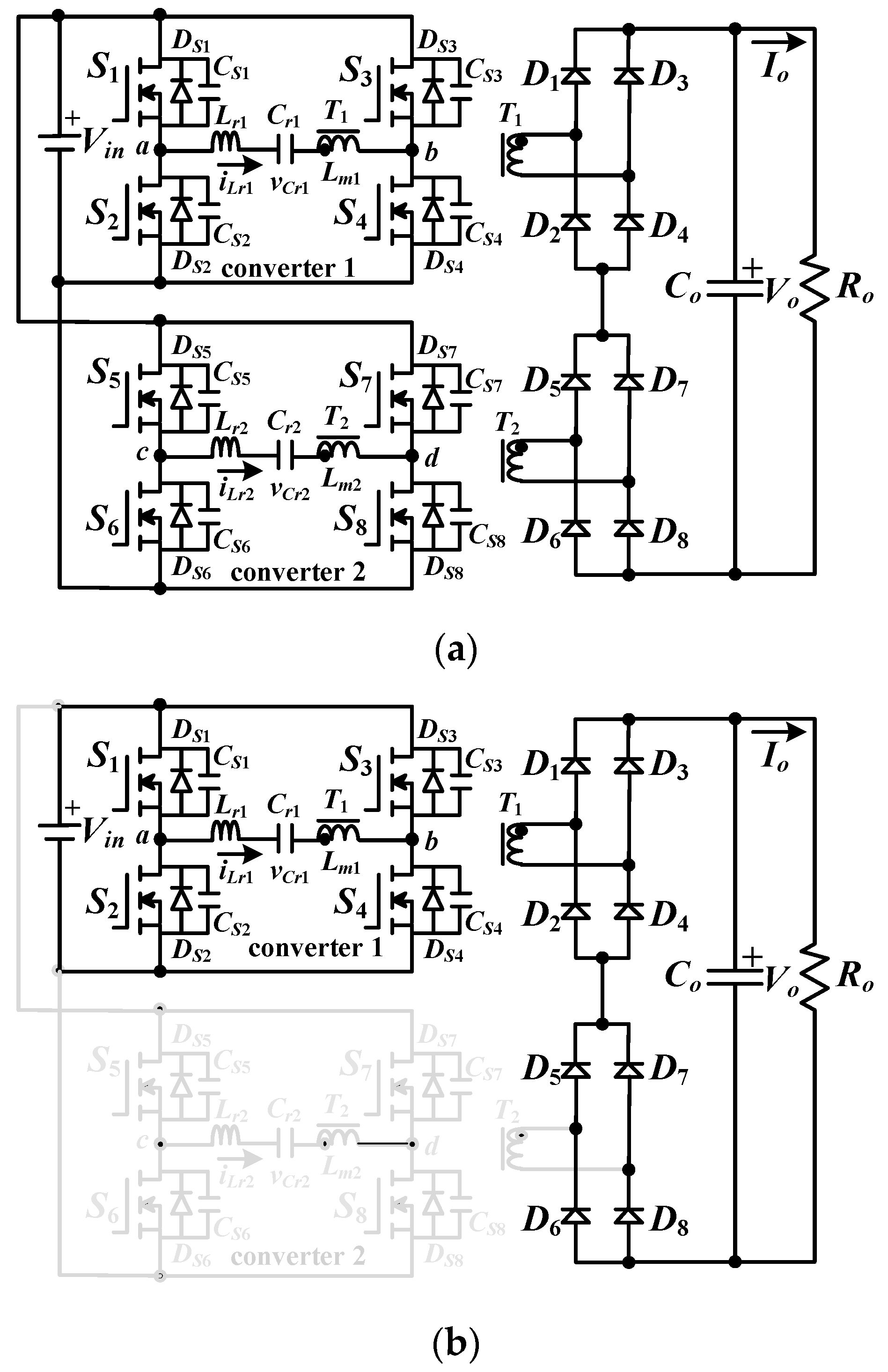
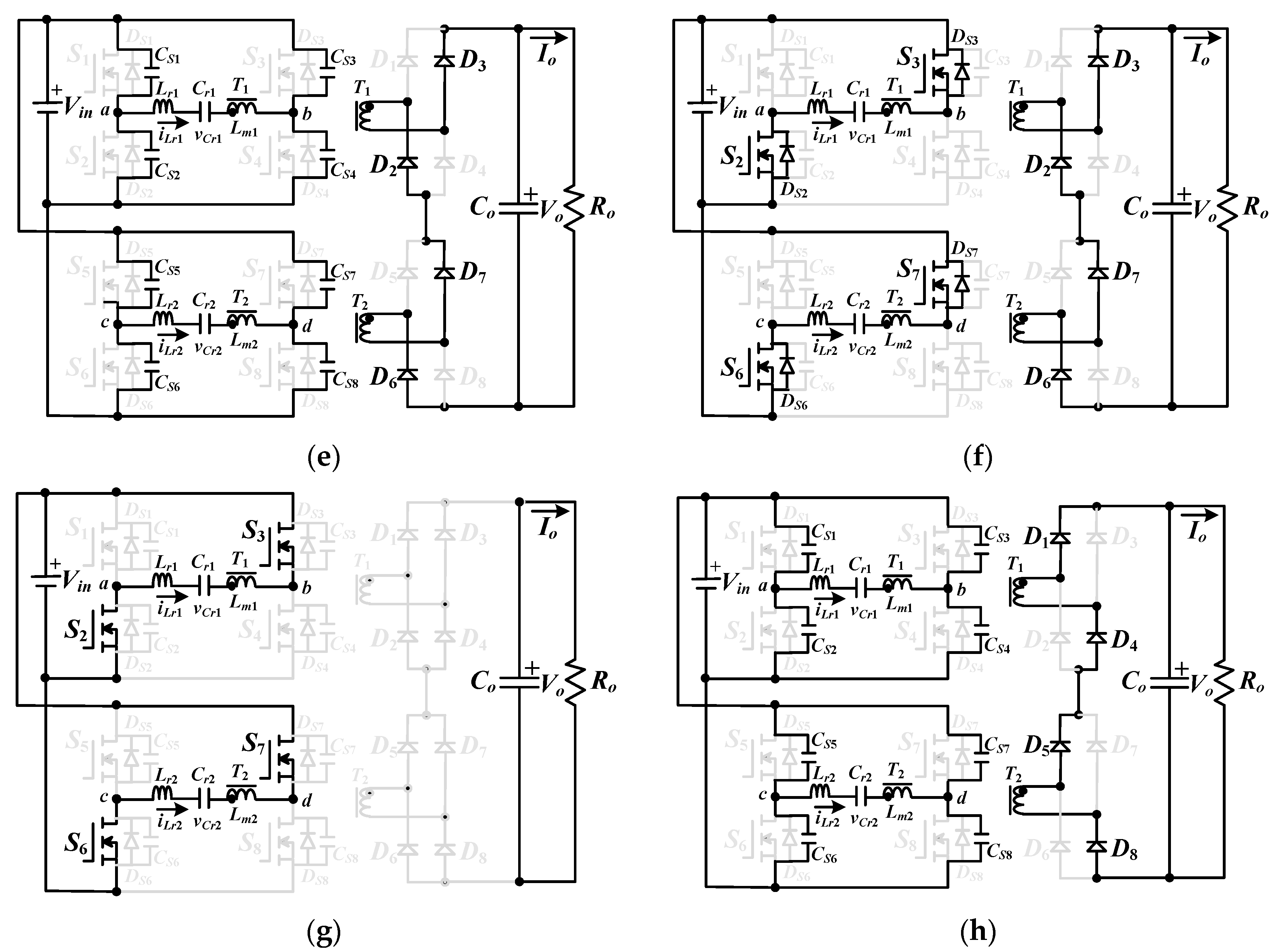
2. Circuit Structure and Operating Principle

The studied converter with wide output voltage operation is illustrated in Figure 1a. Two resonant converters with primary-parallel secondary-series connection are adopted to accomplish the wide voltage operation. Vin is the input voltage. Vo is the output voltage. In each converter, the primary side is a full-bridge resonant structure and the secondary side is the full-bridge diode rectifier. Four power switches are used in the full-bridge resonant structure and four rectifier diodes are employed in the full-bridge rectifier structure. Cr1 and Lr1 are naturally resonant in circuit 1 and Cr2 and Lr2 are resonant in circuit 2. For high-voltage output, two converters are operated and Vo is the summation of the rectified voltages of two full-bridge diode rectifiers shown in Figure 1a. For low-voltage output (Figure 1b), only converter 1 (S1~S4) is controlled and converter 2 (S5~S8) is off. The load voltage Vo equals the rectified voltage of the full-bridge rectifier by D1~D4 and the diodes D5~D8 are forward-biased to bypass the secondary side current of transformer T1. The wide output voltage is achieved in the studied circuit. The frequency control method is adopted to control active devices and adjust the load voltage. The power semiconductors are operated with soft switching characteristics due to the resonant tank having an inductive impedance characteristic.

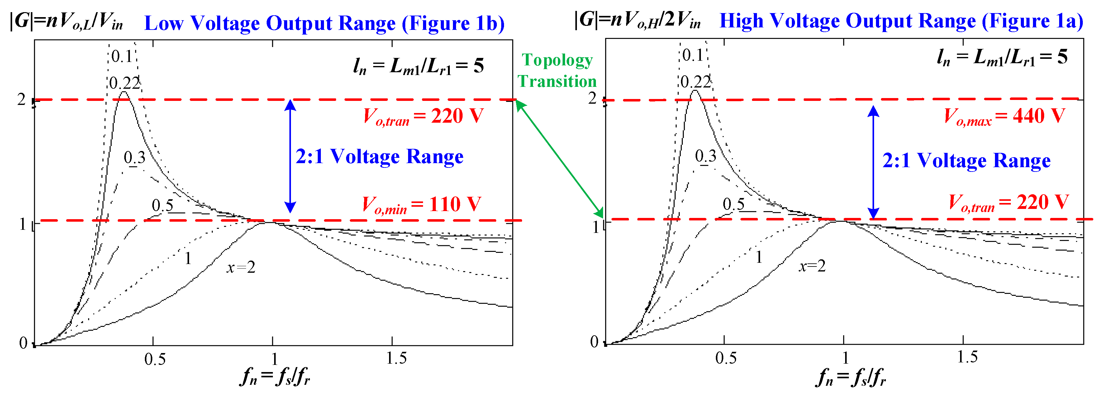
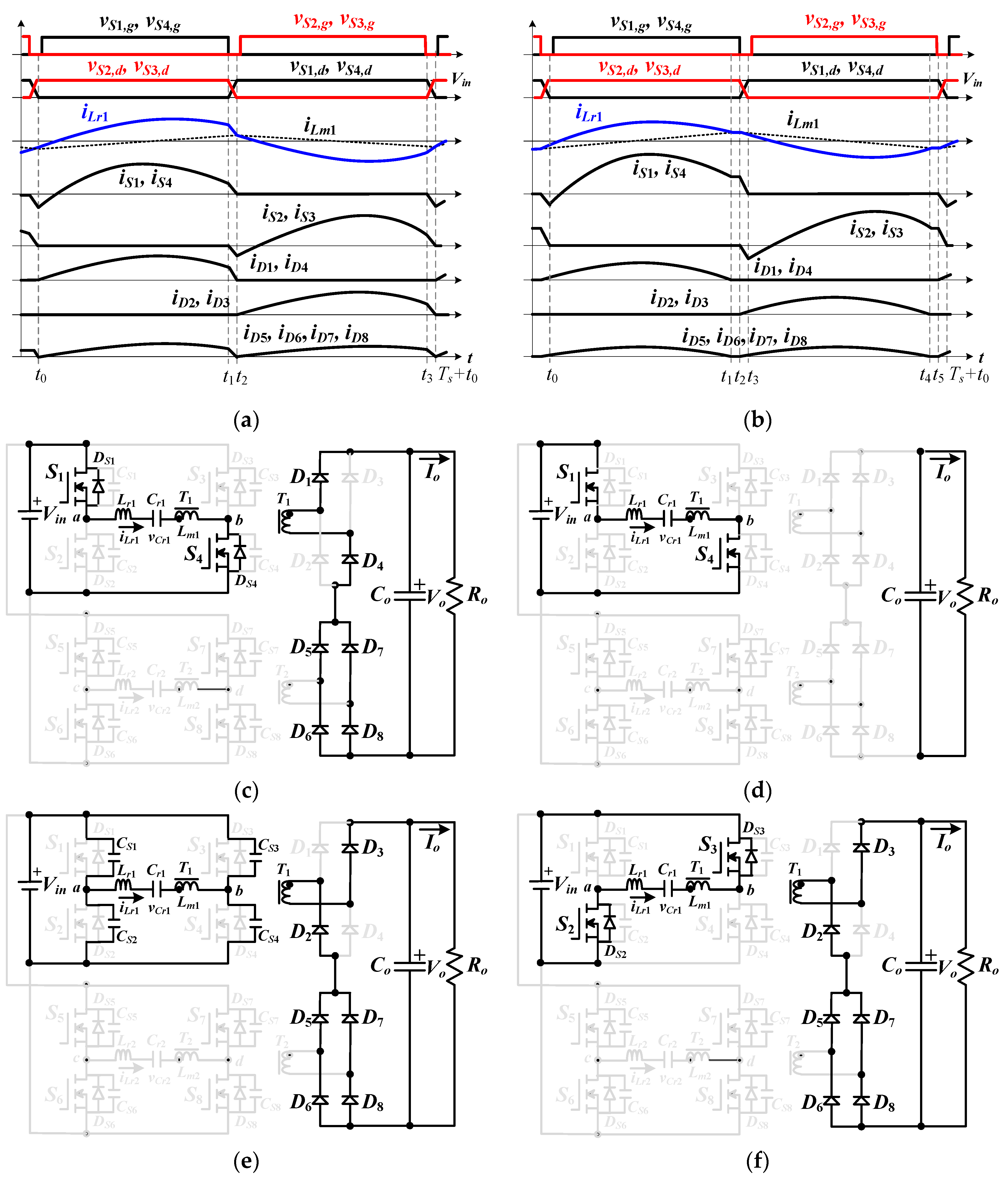
2.1. High-Voltage Output

The resonant converter is controlled by the frequency modulation. If fs (the switching period) > or < fr (series resonant frequency), there are four or six operating modes in every switching period. For high output voltage range, two converters are controlled to increase the load voltage due to the series connection of two full-bridge diode rectifiers at the load side, as shown in Figure 1a. Figure 2a (Figure 2b) illustrates the voltage and current waveforms of the studied converter at high-voltage output under fs > fr (fs < fr) condition. Figure 2c–h demonstrate six equivalent mode circuits at high-voltage output operation and fs < fr (Figure 2b). If fs > fr (Figure 2a), only modes 1, 3, 4, and 6 are operated in a switching cycle.
Mode 1 [t0, t1]: At time t < t0, S1~S8 are off and iLr1 and iLr2 are negative. CS1, CS4, CS5, and CS8 are discharged and CS2, CS3, CS6, and CS7 are charged. At t0, vCS1 = vCS4 = vCS5 = vCS8 = 0. Since iLr1(t0) and iLr2(t0) are all negative value, DS1, DS4, DS5, and DS8 are conducting. S1, S4, S5, and S8 turn on after t0 under zero voltage. Due to D1, D4, D5, and D8 are conducting, vLm1 = vLm2 = nVo/2 where n is the turns ratio of T1 and T2. Cr1 and Lr1 are naturally resonant in converter 1 and Cr2 and Lr2 are resonant in converter 2 with vab = vcd = Vin and vLm1 = vLm2 = nVo/2. The series resonant frequency in mode 1 is f r = 1 / 2 π L r 1 C r 1 . If fs < fr, then iD1, iD4, iD5, and iD8 will be decreased to zero current before S1, S4, S5, and S8 turn off.
Mode 2 [t1, t2]: Owing to fs < fr, iLm1(t1) = iLr1(t1) and iLm2(t1) = iLr2(t1) so that iD1 = iD4 = iD5 = iD8 = 0. No power is delivered to the load resistor. (Lm1, Lr1, and Cr1) and (Lm2, Lr2, and Cr2) are resonant with input voltage vab = vcd = Vin in converters 1 and 2, respectively.
Mode 3 [t2, t3]:S1, S4, S5 and S8 turn off at t2. CS2, CS3, CS6, and CS7 are discharged in mode 2 due to iLr1(t2) > 0 and iLr2(t2) > 0. Since the secondary side currents of T1 and T2 are negative, the diodes D2, D3, D6, and D7 conduct. If the energy stored on (Lr1 and Lm1) and (Lr2 and Lm2) at time t2 is large enough, then the voltages of CS2, CS3, CS6 and CS7 are decreased to zero at t = t3. The resonant currents are calculated in Equation (1):
i L r 1 ( t 2 ) = i L r 2 ( t 2 ) i L m 1 ( t 2 ) = i L m 2 ( t 2 ) = n V o / ( 4 L m f s )
where Lm = Lm1 = Lm2. The soft switching condition of S2, S3, S6, and S7 are given in Equation (2):
i L m 1 ( t 2 ) = i L m 2 ( t 2 ) V i n 4 C e / ( L m + L r )
where Ce = CS1 = … = CS8 and Lr = Lr1 = Lr2. If the dead time td between each switch is given, then the maximum magnetizing inductances are calculated in Equation (3):
L m 1 = L m 2 n V o t d 8 V i n f s C e
Mode 4 [t3, t4]: The voltages of CS2, CS3, CS6, and CS7 are reduced to zero at t3. DS2, DS3, DS6, and DS7 are forward biased owing to iLr1(t3) and iLr2(t3) are positive value. S2, S3, S6, and S7 turn on after t3 with zero voltage condition. In mode 4, D2, D3, D6, and D7 are conducting so that vLm1 = vLm2 = −nVo/2. (Cr1 and Lr1) and (Cr2 and Lr2) are naturally resonant in converters 1 and 2, respectively, with input voltage vab = vcd = −Vin and load voltage vLm1 = vLm2 = −nVo/2. If fs < fr, then iD2, iD3, iD6, and iD7 will be decreased to zero current before S2, S3, S6, and S7 are turned off.
Mode 5 [t4, t5]: Since fs < fr, iLm1 = iLr1 and iLm2 = iLr2 at time t4 and iD2 = iD3 = iD6 = iD7 = 0. No power is transferred to the load resistor. (Lm1, Lr1 and Cr1) and (Lm2, Lr2 and Cr2) are naturally resonant in converters 1 and 2, respectively, with input voltage vab = vcd = −Vin.
Mode 6 [t5, Ts + t0]: At t5, S2, S3, S6, and S7 turn off. Due to iLr1(t5) and iLr2(t5) are negative value, CS1, CS4, CS5, and CS8 are discharged. At time Ts + t0, the voltages of CS1, CS4, CS5, and CS8 are decreased to zero voltage and the studied circuit goes to the next switching cycle operation.

2.2. Low-Voltage Output

For low-voltage output, only S1~S4 are controlled and S5~S8 are off. The secondary side voltage of T1 is connected to the output load and D5~D8 are forward biased, as shown in Figure 1b. Figure 3a,b give the current and voltage waveforms of the studied circuit for low-voltage output under fs > fr and fs < fr conditions, respectively. If fs > fr (Figure 3a), only modes 1, 3, 4, and 6 are operated in a switching cycle. If fs < fr (Figure 3b), there are six equivalent mode circuits (Figure 3c–h) at low-voltage output operation. The operation principle at low-voltage output at fs < fr is presented below.
Mode 1 [t0, t1]:S1~S4 are off and iLr1 < 0 before time t0. CS1 and CS4 discharge by the current iLr1. At time t0, CS1 and CS4 discharge to zero voltage and DS1 and DS4 conduct. The drain-to-source voltages vS1,d = vS4,d = 0 and S1 and S4 turn on after t0 under zero voltage condition. In mode 1, the load current flows through D1, Co, Ro, D5~D8 and D4. The magnetizing inductor voltage vLm1 = nVo. Cr1 and Lr1 are naturally resonant with vab = Vin and vLm1 = nVo. If fs < fr, then iD1, iD4, and iD5~iD8 will be reduced to zero before S1 and S4 turn off.
Mode 2 [t1, t2]: Due to fs < fr, iLm1 = iLr1 at time t1 so that D1~D8 are off on the output side. Lr1, Cr1, and Lm1 are naturally resonant with Vab = Vin. If fsfr, the peak-to-peak magnetizing current ΔiLm1 during one-half of switching period approximates:
Δ i L m 1 ( t ) n V o 2 L m f s
Mode 3 [t2, t3]: At time t2, S1 and S4 turn off. Owing to iLr1 > 0, the voltages of CS2 and CS3 are decreased. If the current iLr1(t2) ≈ ΔiLm1/2 is large enough, then the voltages of CS2 and CS3 will be decreased to zero at t3.
Mode 4 [t3, t4]: At t3, vCS2 = vCS3 = 0 and DS2 and DS3 conduct. S2 and S3 turn on after t3 under zero voltage. The load current flows through D3, Co, Ro, D5~D8, and D2 so that vLm1 = −nVo. In mode 4, Cr1 and Lr1 are naturally resonant with vab = −Vin and vLm1 = −nVo in mode 4. If fs < fr, then iD2, iD3, and iD5~iD8 decrease to zero current before S2 and S3 turn off.
Mode 5 [t4, t5]: At t4, iLm1 = iLr1 so that D1~D8 are reverse biased. Lr1, Cr1, and Lm1 are resonant with vab = −Vin. Mode 5 ends at t5 when S2 and S3 turn off.
Mode 6 [t5, Ts + t0]: At t5, S2 and S3 turn off. Owing to iLr1 < 0, CS1 and CS4 are discharged by iLr1. At time Ts + t0, vCS1 = vCS4 = 0.

3. Circuit Characteristics and Design Guidelines

The load voltage control is based on the frequency modulation against line and load regulations. To ignore the harmonic components, the fundamental harmonic frequency approach is used to estimate the AC voltage gain of the studied circuit. The wide voltage operation is accomplished by selecting the series connections of two full-bridge diode rectifiers for high-voltage output (Figure 1a) or only one diode rectifier for low-voltage operation (Figure 1b). Since S1~S8 have the Ts/2 turn-on time, the AC voltages vab and vcd are square voltage waveforms with voltage values ±Vin. The fundamental root-mean-square (rms) voltages Vab,rms and Vcd,rms are calculated in Equation (5):
V a b , r m s = V c d , r m s = 2 2 V i n / π
For high-voltage output, two full-bridge diode rectifiers are series-connected and connect to the output load. The magnetizing voltages vLm1 = vLm2 = ±nVo/2. For low-voltage output, only one full-bridge connects to the output load and the magnetizing voltage vLm1 = ±nVo and vLm2 = 0. The fundamental rms magnetizing voltages VLm1,rms and VLm2,rms are calculated as:
V L m 1 , r m s = { 2 n V o , H / π ,   for   high   voltage   output 2 2 n V o , L / π ,   for   low   voltage   output
V L m 2 , r m s = { 2 n V o , H / π ,   for   high   voltage   output 0 ,   for   low   voltage   output
where Vo,L and Vo,H denote the output voltage Vo at the low and high voltage ranges, respectively. From the given DC load resistor Ro, the equivalent primary side resistors Rac1 and Rac2 of T1 and T2 are calculated in Equations (8) and (9):
R a c 1 = { 4 n 2 R o π 2 ,   for   high   voltage   output 8 n 2 R o π 2 ,   for   low   voltage   output
R a c 2 = 4 n 2 R o π 2 ,   for   high   voltage   output
Based on the resonant circuit, the transfer function of the studied circuit is calculated in Equation (10):
| G | = V L m 1 , r m s V a b , r m s = 1 [ 1 + 1 l n f n 2 1 f n 2 ] 2 + x 2 ( f n 2 1 f n ) 2   = { n V o , H 2 V i n ,   for   high   voltage   output n V o , L V i n ,   for   low   voltage   output
where fn = fs/fr is the frequency ratio, ln = Lm1/Lr1 is the inductor ratio, and x = L r 1 / C r 1 / R a c 1 is the quality factor. The output voltage at high and low output voltage range can be re-written in Equations (11) and (12):
V o , H = 2 V i n n [ 1 + 1 l n f n 2 1 f n 2 ] 2 + x 2 ( f n 2 1 f n ) 2  
V o , L = V i n n [ 1 + 1 l n f n 2 1 f n 2 ] 2 + x 2 ( f n 2 1 f n ) 2  
Based on the output voltage range, S1~S8 are regulated with variable frequency control to accomplish the wide voltage range output capability. Due to the resonant circuit always being controlled at the inductive impedance load, S1~S8 will be operated under the soft switching condition.
To confirm the theoretical analysis, the design guideline of a laboratory circuit is provided. The electrical specifications of the prototype circuit are Vin = 380 V and Vo = 110 V~440 V (4:1 voltage ratio). The rated output power is 1000 W (200 W) for low (high)-voltage output and fr = 100 kHz. To accomplish wide voltage output operation (4:1), two full-bridge resonant converters with input-parallel output-series connection are employed under the high output voltage range Vo,H = 220 V~440 V. However, only converter 1 is operated for low-voltage output Vo,L = 110 V~220 V. The voltage gain of the studied circuit with wide output voltage operation Vo = 110 V~440 V under the Vin = 380 V condition is provided in Figure 4. The transient voltage (Vo,tran) between two resonant converters’ operation and one resonant converter operation is 220 V with ±5 V voltage tolerance using a Schmitt trigger comparator, as shown in Figure 5. Since the voltage gain of the studied circuit in the low-voltage output range is two times the voltage gain in the high-voltage output range in Equation (10), two resonant converters’ operation for high-voltage output (Figure 1a) and one resonant converter operation for low-voltage output (Figure 1b) have the same design procedure due to Vo,H = 2Vo,L in Equations (11) and (12). Only one resonant converter is designed for the low-voltage output case to simplify the design guideline. For the low-voltage output case, the minimum voltage gain Gmin is equal to unity at 110 V output voltage. The turns ratio n of T1 can be obtained from Equation (13):
n = G min V i n V o , L , min = 1 × 380   V 110   V 3.455
TDK (Tokyo Denki Kagaku, Tokyo, Japan) EE-55 magnetic cores with flux density ΔB = 0.4 T and Ae = 3.54 cm2 are adopted to implement transformers T1 and T2. The minimum switching frequency in the studied circuit is assumed at 60 kHz under Vo,tran output. The minimum primary winding turns are obtained in Equation (14):
N p 1 , min n V o , t r a n 2 f s , min Δ B A e = 3.455 × 220   V 2 × 60000   H z × 0.4   T × 3.54 × 10 4   m 2 45
In the prototype circuit, the actual transformer winding turns of T1 and T2 are Np1 = Np2 = 45 and Ns1 = Ns2 = 13. The equivalent primary side resistance Rac1 under Po,max = 1000 W and Vo,L,min = 110 V is calculated in Equation (15):
R a c 1 = 8 n 2 π 2 R o , r a t e d = 8 × ( 45 / 13 ) 2 π 2 × ( 110   V ) 2 1000   W 117.5   Ω
In the prototype circuit, the selected parameters ln = 5 and x = 0.2. The resonant components Lr1, Lr2, Lm1, Lm2, Cr1, and Cr2 are calculated as:
L r 1 = L r 2 = x R a c 1 2 π f r = 0.2 × 117.5   Ω 2 π × 100 × 10 3   Hz 37.4   μ H
L m 1 = L m 2 = l n L r 1 = 37.4 × 5   μ H = 187   μ H
C r 1 = C r 2 = 1 4 π 2 L r 1 f r 2 = 1 4 π 2 × 37.4 × 10 6   F × ( 100 × 10 3   Hz ) 2 68   nF
The voltage ratings of D1~D8 are equal to Vo,max/2 = 220 V. The voltage ratings of S1~S8 are Vin = 380 V. Power switches SiHG20N50C (500 V/ 11A) are employed for S1~S8 and SBR20A300CTFP (300 V/20 A) are used for D1~D8. The selected output capacitance Co = 720 μF/450 V. The frequency modulation controller UCC25600 is adopted to generate the gating signals of S1~S8.

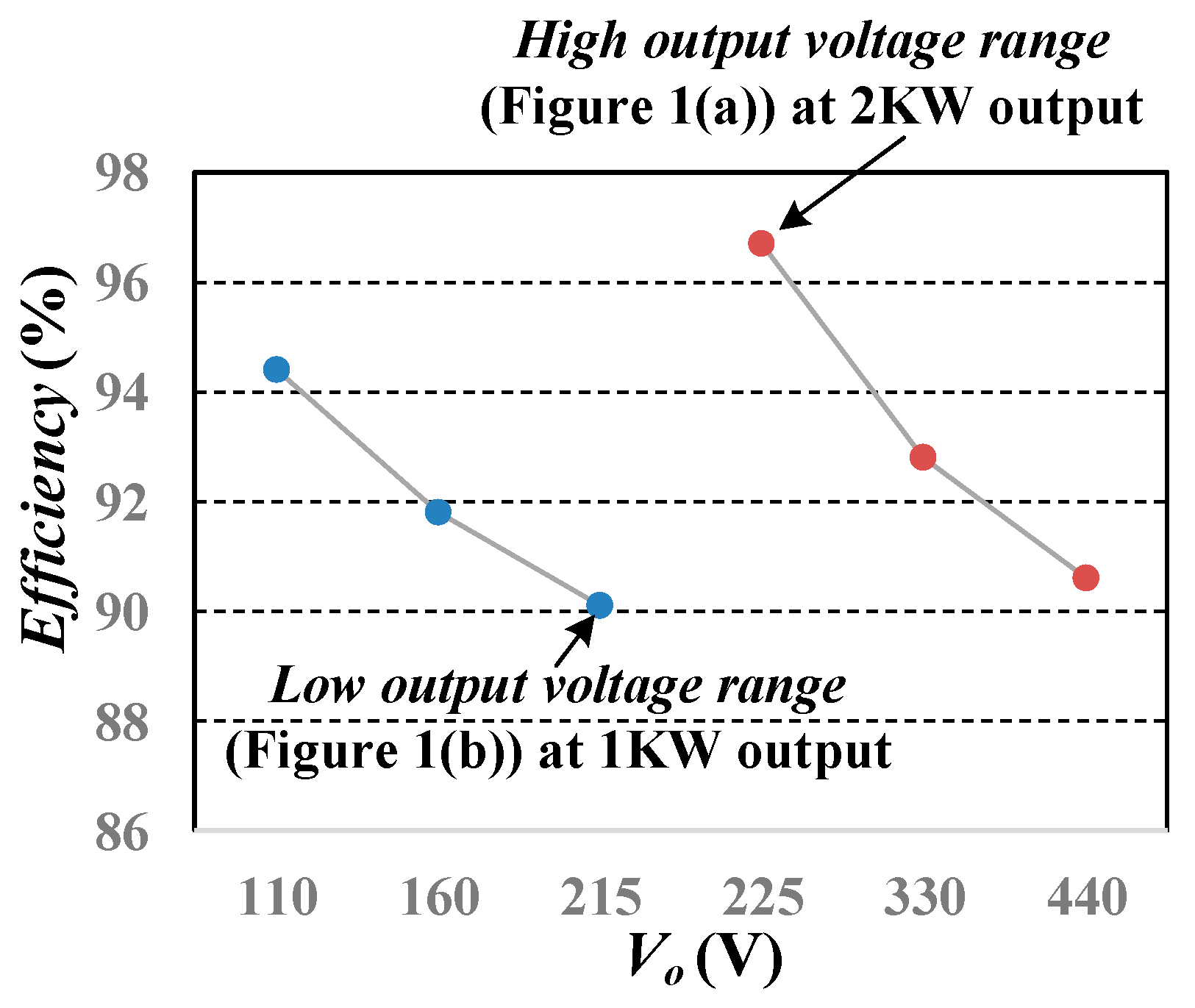
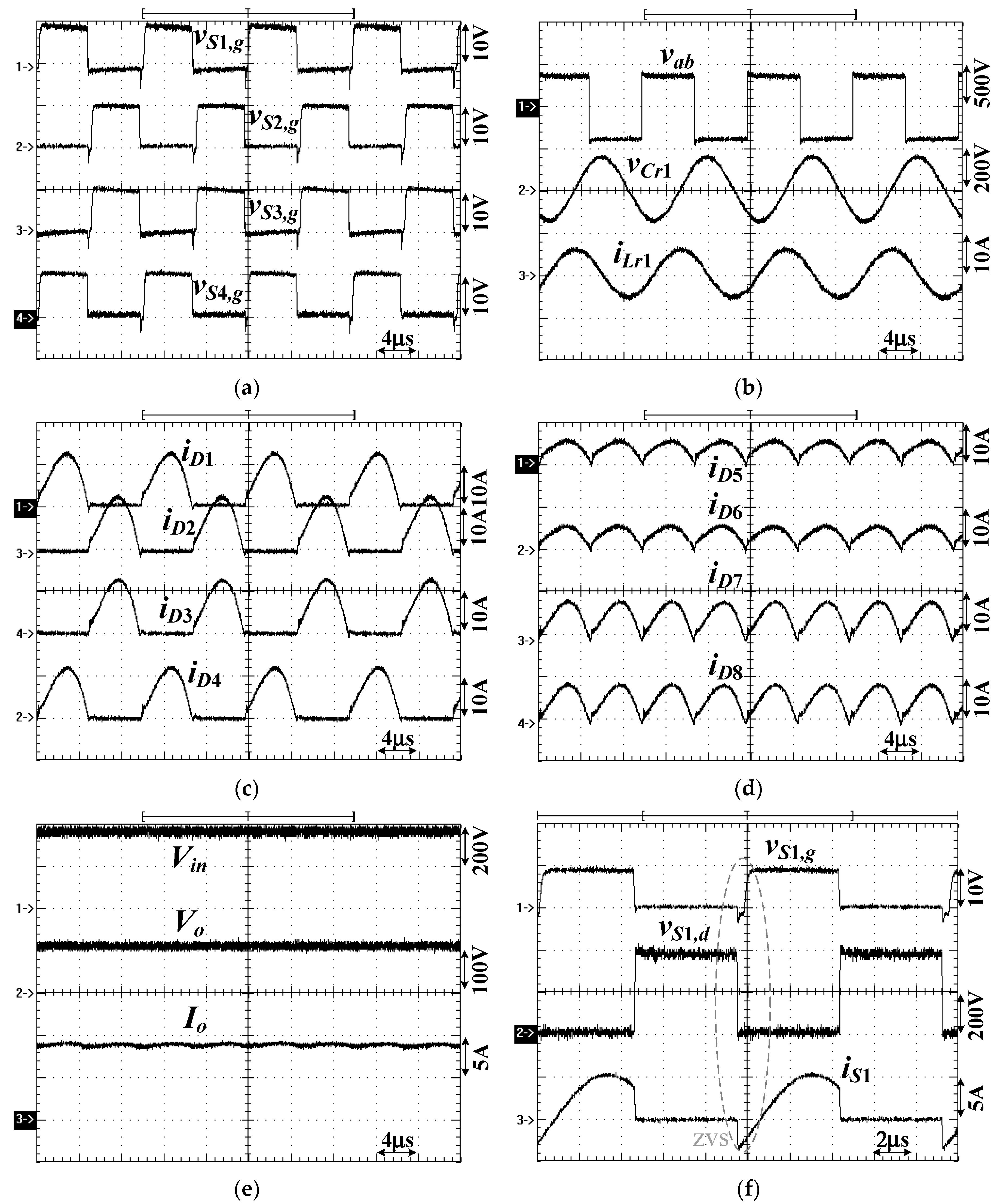
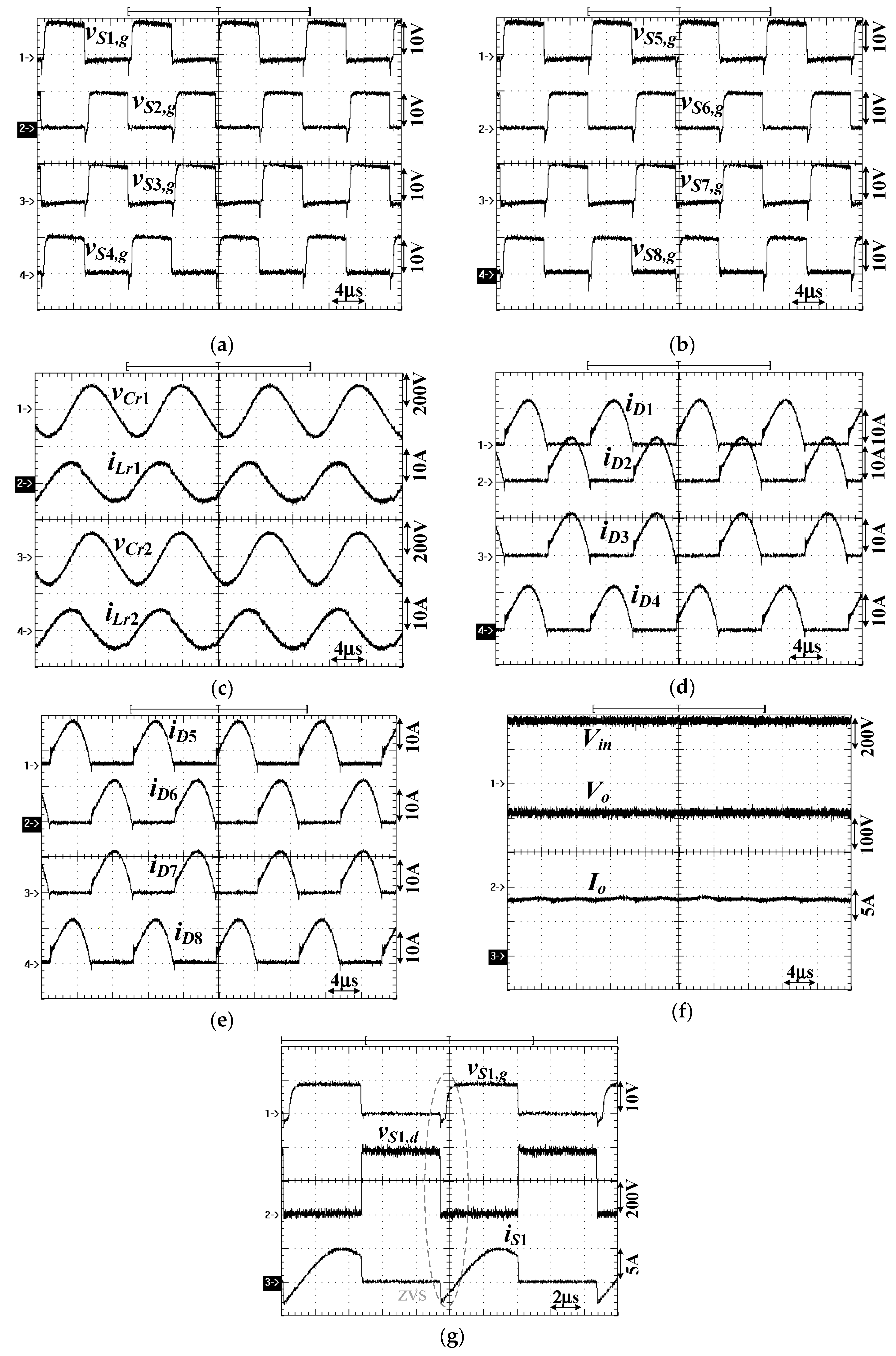
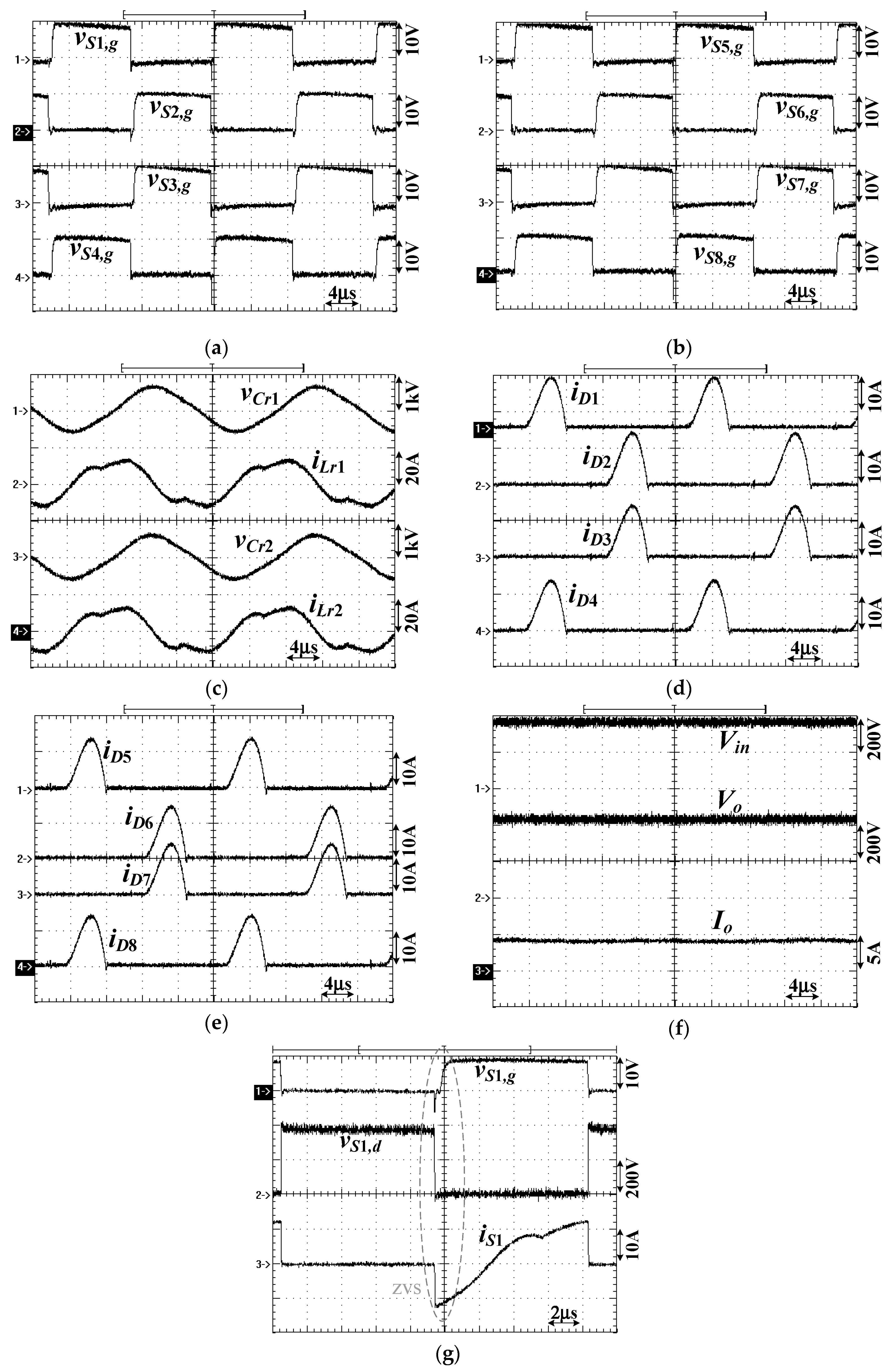
4. Experimental Verification

A laboratory prototype (Figure 6) was constructed and tested. The circuit parameters are calculated from the previous section. The test waveforms are demonstrated and shown to confirm the theoretical discussion and effectiveness of the studied circuit with a wide output voltage range. Figure 7 and Figure 8 provide the experimental results under low-voltage range with only one resonant converter operation. Figure 7 demonstrates the experimental waveforms for Vo = 110 V and Po = 1 kW. The experimental waveforms of vS1,g~vS4,g are given in Figure 7a. The switching frequency of S1~S4 is about 100 kHz. The leg voltage vab and the resonant component waveforms vCr1 and iLr1 are provided in Figure 7b. vCr1 and iLr1 are almost sinusoidal waveforms due to fs ≈ fr. The inductor current iLr1 is lagging to the measured voltage vab. The input impedance of the resonant tank by Cr1, Lr1, Lm1, and Rac1 is operated at the inductive load. Figure 7c,d provide the measured diode currents. It is obvious that D1~D4 turn off under zero current. There is a slight current imbalance on D5 and D7 due to the unequal PCB layout length of D5 and D7. Figure 7e provides the test results of Vin, Vo, and Io. The output voltage Vo is controlled at 110 V output and the load current is 9.1 A. Figure 7f shows the experimental waveforms vS1,g, vS1,d, and iS1. It is observed that the drain voltage vS1,d is decreased to zero before S1 turns on. The zero-voltage turn-on switching of switch S1 is achieved in Figure 7f. S2~S4 have the same turn-on characteristic as S1. It can be expected that the zero-voltage turn-on switching of S2~S4 is also implemented.
Figure 8 provides the measured results for Vo = 215 V and Po = 1 kW. The experimental waveforms vS1,g~ vS4,g are given in Figure 8a and the switching frequency is about 57 kHz. Comparing the test results in Figure 7a and Figure 8a, the switching frequency under Vo = 215 V is lower than the switching frequency under the Vo = 110 V case. Figure 8b illustrates the measured signals of vab, vCr1, and iLr1. iLr1 is a quasi-sinusoidal waveform due to fs < fr under Vo = 215 V. The inductor current iLr1 is lagging the measured voltage vab. The input impedance of the resonant tank by Cr1, Lr1, Lm1, and Rac1 is operated at the inductive load. The measured diode currents on the output side are provided in Figure 8c,d. It can be observed that D1~D4 turns off under zero current. The measured waveforms of Vin, Vo, and Io are provided in Figure 8e. Figure 8f shows the experimental waveforms vS1,g, vS1,d, and iS1. It is clear that vS1,d is decreased to zero before S1 turns on. The zero-voltage turn-on switching of S1 is achieved in Figure 8f for Vo = 215 V condition.
Figure 9 and Figure 10 give the measured waveforms for the high-voltage output range. Two full-bridge resonant converters with primary-parallel secondary-series connection are controlled in the presented converter to provide high-voltage output. Figure 9 provides the experimental results at Vo = 225 V and Po = 2000 W. Figure 10 gives the experimental waveforms at 440 V output voltage and 2 kW output power. Figure 9a,b provide the waveforms of S1~S8 and the switching frequency is about 106 kHz. Figure 9c provides the capacitor voltages and inductor currents of two full-bridge resonant converters. The voltage and current waveforms on two full-bridge circuits are balanced well. The measured diode currents on the secondary sides are demonstrated in Figure 9d,e and the diode currents iD1~iD8 of two full-bridge diode rectifiers are also balanced well. Figure 9f provides the measured results of Vin, Vo, and Io. The measured voltage Vo = 225 V and Io = 8.8 A. The experimental waveforms vS1,g, vS1,d, and iS1 are given in Figure 9g. Before S1 is turned on, vS1,d is decreased to zero. The soft switching turn-on of S1 is realized for Vo = 225 V case. The switch signals S1~S4 and S5~S8 are demonstrated in Figure 10a,b under Vo = 440 V and Po = 2 kW conditions. The switching frequency is about 59 kHz. The experimental results of vCr1, vCr2, iLr1, and iLr2 are shown in Figure 10c. It is clear that capacitor voltages vCr1 and vCr2 and inductor currents iLr1 and iLr2, iLr1, and iLr are well balanced. The diode currents iD1~iD4 and iD5~iD8 are provided in Figure 10d,e, respectively. It can be observed that iD1~iD4 and iD5~iD8 are well balanced. The measured waveforms of Vin, Vo, and Io are provided in Figure 10f under Vo = 440 V and Io = 4.6 A. The experimental waveforms vS1,g, vS1,d, and iS1 are given in Figure 10g. Before S1 is turned on, the drain voltage vS1,d has been decreased to zero. The soft switching turn-on of S1 is achieved for the Vo = 400 V case.
Figure 11 shows the measured efficiencies of the proposed converter under different output voltages and rated power. The test efficiencies of the presented circuit are 94.4% at Vo = 110 V under Po = 1 kW (low output voltage range), 90.1% at Vo = 215 V under Po = 1 kW (low output voltage range), 96.7% at Vo = 225 V under Po = 2 kW (high output voltage range) and 90.6% at Vo = 440 V under Po = 1 kW (high output voltage range). From the test results, it can be observed that the circuit efficiency in the low-voltage case Vo = 110 V (Vo = 225 V) is better than the high-voltage case Vo = 215 V (Vo = 440 V) for low output voltage range (high output voltage range). The switching period at Vo = 215 V is greater than the switching period at Vo = 110 V. Due to the magnetizing current loss, which depended on the output voltage and the switching period, the estimated power loss from the magnetizing current at Vo = 215 V output is greater than the Vo = 110 V case. Therefore, the measured efficiency of the studied converter at Vo = 110 V is better than the Vo = 215 V output. Similarly, the measured circuit efficiency at Vo = 225 V is better than the Vo = 440 V output. Comparing the circuits shown in Figure 1, it can be observed that one full-bridge resonant converter and eight rectifier diodes are operated for the low-voltage output case, and two full-bridge resonant converters and eight rectifier diodes are operated for the high-voltage output case. It is clear that there are more conduction losses on diodes D5~D8 for the low-voltage output. The power losses on these diodes are equal to 2VfIo, where Vf is the voltage drop on D5~D8. The percentage between the power loss on diodes D5~D8 and the rated power is about 2Vf/Vo. Since Vo >> Vf, it can be expected that this extra power loss on diodes D5~D8 will not result in serious problems. Due to the Vf = 0.9 V for diodes SBR20A300CTFP, the calculated power loss percentage on diodes D5~D8 is about 1.6% in the 110 V output case and 0.8% in the 215 V output case.

5. Conclusions

A new resonant circuit with a series-parallel structure is presented in this paper to achieve the benefits of low switching loss, wide output voltage capability, and low-voltage rating on rectifier diodes. In the proposed converter, two diode rectifiers with series-connection are employed on the secondary side to reduce the voltage rating on the rectifier diodes for high output voltage range operation. The voltage rating of rectifier diodes is Vo,max/2 instead of the Vo,max voltage rating in conventional resonant converters. Since the proposed resonant tank is operated under the inductive load condition, the soft switching operation can be implemented in the studied converter. Finally, a 2 kW laboratory circuit was constructed and experiments are demonstrated to confirm the usefulness of the presented hybrid resonant converter for wide voltage output capability.

Author Contributions

B.-R.L. proposed and designed this project and was responsible for writing the paper.

Funding

This research is funded by the Ministry of Science and Technology, Taiwan, under grant number MOST 108-2221-E-224-022-MY2.

Acknowledgments

This research is supported by the Ministry of Science and Technology, Taiwan, under contract MOST 108-2221-E-224-022-MY2. The author would like to thank Mr. H. R. Cheng for his help to measure the circuit waveforms in the experiment.

Conflicts of Interest

The author declares no potential conflict of interest.

References

  1. Wang, Y.; Zhang, S.; Guan, Y.; Liu, X.; Xu, D. Single-stage QR ac-dc converter based on buck-boost and flyback circuits. IET Power Electron. 2017, 10, 103–111. [Google Scholar] [CrossRef]
  2. Xie, X.; Li, J.; Peng, K.; Zhao, C.; Lu, Q. Study on the single-stage forward-flyback PFC converter with QR control. IEEE Trans. Power Electron. 2016, 31, 430–442. [Google Scholar] [CrossRef]
  3. Lin, B.R.; Chiang, H.K.; Chen, C.C. Analysis and implementation of a zvs-pwm converter with series-connected transformers. IEEE Trans. Circuits Syst. II 2007, 54, 917–921. [Google Scholar] [CrossRef]
  4. Singh, A.K.; Das, P.; Panda, S.K. Analysis and design of SQR-based high-voltage LLC resonant dc-dc converter. IEEE Trans. Power Electron. 2017, 32, 4466–4481. [Google Scholar] [CrossRef]
  5. Haga, H.; Kurokawa, F. Modulation method of a full-bridge three-level LLC resonant converter for battery charger of electric vehicles. IEEE Trans. Power Electron. 2017, 32, 2498–2507. [Google Scholar] [CrossRef]
  6. Steigerwald, R.L. A comparison of half-bridge resonant converter topologies. IEEE Trans. Power Electron. 1988, 3, 174–182. [Google Scholar] [CrossRef]
  7. Lin, B.R.; Lin, Y. Parallel current-fed resonant converter with balance current sharing and no input ripple current. IET Power Electron. 2019, 12, 212–219. [Google Scholar] [CrossRef]
  8. Safaee, A.; Jain, P.; Bakhshai, A. A ZVS pulsewidth modulation full-bridge converter with a low-RMS-current resonant auxiliary circuit. IEEE Trans. Power Electron. 2016, 31, 4031–4047. [Google Scholar] [CrossRef]
  9. Liu, P.J.; Hsu, Y.C.; Hsu, S.R. Drain-voltage balance and phase-shifted PWM control schemes for high-efficiency parallel-string dimmable LED drivers. IEEE Trans. Ind. Electron. 2018, 65, 6168–6176. [Google Scholar] [CrossRef]
  10. Lee, I.O.; Moon, G.W. Phase-shifted PWM converter with a wide ZVS range and reduced circulating current. IEEE Trans. Power Electron. 2013, 28, 908–919. [Google Scholar] [CrossRef]
  11. Mishima, T.; Akamatsu, K.; Nakaoka, M. A high frequency-link secondary-side phase-shifted full-bridge soft-switching PWM DC-DC converter with ZCS active rectifier for EV battery charged. IEEE Trans. Power Electron. 2013, 28, 5758–5773. [Google Scholar] [CrossRef]
  12. Li, Z.; Wu, T.; Zhang, G.; Yang, R. High modulation method combining variable frequency and double phase-shift for a 10 kW LLC resonant converter. IET Power Electron. 2018, 11, 2161–2169. [Google Scholar] [CrossRef]
  13. Pahlevani, M.; Pan, S.; Jain, P. A hybrid phase-shift modulation technique for DC/DC converters with a wide range of operating conditions. IEEE Trans. Ind. Electron. 2016, 63, 7498–7510. [Google Scholar] [CrossRef]
  14. Jovanović, M.M.; Irving, B.T. On the fly topology-morphing control efficiency optimization method for LLC resonant converters operating in wide input and/or output-voltage range. IEEE Trans. Power Electron. 2016, 31, 2596–2608. [Google Scholar] [CrossRef]
  15. Zhang, C.; Gao, Z.; Liao, X. Bidirectional dc-dc converter with series-connected resonant tanks to realize soft switching. IET Power Electron. 2018, 11, 2029–2043. [Google Scholar] [CrossRef]
  16. Sun, W.; Xing, Y.; Wu, H.; Ding, J. Modified high-efficiency LLC converters with two split resonant branches for wide input-voltage range applications. IEEE Trans. Power Electron. 2018, 33, 7867–7870. [Google Scholar] [CrossRef]
Figure 1. Circuit configuration of the studied circuit (a) for high-voltage output operation, and (b) for low-voltage output operation.
Energies 12 03479 g001
Figure 2. Circuit waveforms and equivalent mode circuits at high-voltage output. (a) PWM waveforms when fs > fr; (b) PWM waveforms when fs < fr; (c) mode 1; (d) mode 2; (e) mode 3; (f) mode 4; (g) mode 5; and (h) mode 6.
Energies 12 03479 g002aEnergies 12 03479 g002b
Figure 3. Circuit waveforms and equivalent mode circuits at low-voltage output. (a) PWM waveforms when fs > fr; (b) PWM waveforms when fs < fr; (c) mode 1; (d) mode 2; (e) mode 3; (f) mode 4; (g) mode 5; and (h) mode 6.
Energies 12 03479 g003aEnergies 12 03479 g003b
Figure 4. Gain curves of the studied circuit with output voltage Vo = 110 V~440 V and input voltage Vin = 380 V.
Energies 12 03479 g004
Figure 5. Control block of voltage transition operation. (a) Schmitt comparator; and (b) control block of signals S1~S8.
Energies 12 03479 g005
Figure 6. Picture of the proposed converter.
Energies 12 03479 g006
Figure 7. Measured results at 110 V output and 1 kW load under the low output voltage range. (a) PWM signals vS1,g~vS4,g; (b) vab, vCr1, iLr1; (c) diode currents iD1~iD4;(d) diode currents iD5~iD8; (e) Vin, Vo, Io; and (f) vS1,g, vS1,d, iS1.
Energies 12 03479 g007
Figure 8. Measured results at 215 V output and 1 kW load under the low output voltage range. (a) PWM signals vS1,g~vS4,g; (b) vab, vCr1, iLr1; (c) diode currents iD1~iD4;(d) diode currents iD5~iD8; (e) Vin, Vo, Io; and (f) vS1,g, vS1,d, iS1.
Energies 12 03479 g008
Figure 9. Measured results at 225 V output and 2 kW load under the high output voltage range. (a) PWM signals vS1,g~vS4,g; (b) PWM signals vS5,g~vS8,g; (c) vCr1, iLr1, vCr2, iLr2; (d) diode currents iD1~iD4;(e) diode currents iD5~iD8; (f) Vin, Vo, Io; and (g) vS1,g, vS1,d, iS1.
Energies 12 03479 g009
Figure 10. Measured results at 440 V output and 2 kW load under a high output voltage range. (a) PWM signals vS1,g~vS4,g; (b) PWM signals vS5,g~vS8,g (c) vCr1, iLr1, vCr2, iLr2; (d) diode currents iD1~iD4;(e) diode currents iD5~iD8; (f) Vin, Vo, Io; and (g) vS1,g, vS1,d, iS1.
Energies 12 03479 g010
Figure 11. Measured circuit efficiencies of the proposed converter under different output voltages and the rated power.
Energies 12 03479 g011

