Article

A Family of Y-Impedance-Network Half-Bridge Converters with Additional Voltage Adjustment Function

1
School of Automation, Guangdong University of Technology, Guangzhou 510006, China
2
School of Automation, Foshan University, Foshan 528000, China
*
Author to whom correspondence should be addressed.
Energies 2019, 12(18), 3430; https://doi.org/10.3390/en12183430
Submission received: 6 August 2019 / Revised: 26 August 2019 / Accepted: 4 September 2019 / Published: 5 September 2019

Abstract

:
Half-bridge converters have been widely used in multiple medium power level applications because of the advantages of having less switches and being easy to control. However, their inherent structure leads to low output amplitude and shoot-through problems. In this study, we propose a family of novel half-bridge converters implementing a Y-impedance-network with additional buck-boost voltage adjustment function with the aim of resolving these issues. In order to verify the effectiveness of the proposed topologies, simulations and experiments were conducted, the results which well validate the feasibility of the proposed converters.

1. Introduction

In terms of reducing the loss of transmission, building integrated photovoltaic (BIPV) systems reduce costs and increase efficiency as compared to a centralized PV plant [1], however they require high reliability, low cost, and high voltage gain. Traditional inverters are buck-type converters which can no longer satisfy BIPV requirements. Additionally, they are vulnerable to electromagnetic interference because their bridge, which contains series switches, can easily short-circuit with strong current of shoot-through. In order to increase the voltage gain, a traditional solution is to cascade a voltage pumping structure with only a few passive elements [2,3]. However, it results in low efficiency. Owing to their high efficiency, single-state inverters have been widely used which usually combine a transformer or passive elements into traditional inverters to achieve a higher voltage gain [2,4,5]. However, adding a transformer results in a bulky volume and low efficiency. Moreover, this solution has a narrow window of voltage adjustment since the transformer only has a fixed voltage ratio. Furthermore, they work under the threat of a shoot-through which leads to the need for controlling strategies. To provide an effective method to solve the shoot-through problem and increase output voltage systematically, the authors in [6] proposed an L C network named a Z-source inverter (ZSI), which performs a boost function and prevents components being destroyed when working during a shoot-through. However, applying a Z-source into a half-bridge inverter leads to the problem of an imbalance at the midpoint voltage of the input capacitors. Targeting this issue, authors in [7] proposed a novel Z-source half-bridge converter which also realizes buck-boost function. However, with a fixed structure, ZSI or quasi-Z-source inverter (qZSI) cannot realize a high enough voltage gain, which is a requirement in BIPV. Magnetic coupling is an effective method to improve the performance and efficiency. Many magnetically coupled impedance networks have been explored, such as T-source [8,9], Trans-Z-source [10], Γ -Z-source [11], flipped- Γ -Z-source [12], and A-source [13]. Their different winding placements lead to different advantages and applications. Combining their advantages, a Y-source impedance network (also known as a Y-impedance-network) is proposed which has higher voltage gain and a smaller size with less passive components [14]. However, there is a severe problem: the existence of pulsed input currents. Addressing this issue, quasi-Y-source inverters with an additional inductor are proposed in [15,16,17], and they also have additional voltage gain. However, they can only vary voltage gain by adjusting the turns ratio and duty cycle which cannot meet special industrial requirements. Under the premise of solving the pulsed input currents problem, an improved quasi-Y-source converter was proposed with higher voltage gain [18]. However, the additional switch leads to difficultly regarding control.
In order to increase voltage gain and provide more degrees of adjustment to vary the voltage, the additional inductor in [15] is replaced by a general step-up cell. Combining the advantages of half-bridge converters and a Y-impedance network, we propose a novel family of high step-up Y-impedance-network half-bridge converters, coupled with a general step-up cell for additional voltage adjustment to solve the above problems.
The rest of this paper is organized as follows. Detailed descriptions and analyses of the proposed converters are given in Section 2. In Section 3, the proposed converter and conventional Z-source half-bridge converter are compared to demonstrate the unique features of the proposed solution. In Section 4 and Section 5, the simulation and experimental studies are presented. Finally, a conclusion is drawn in Section 6.

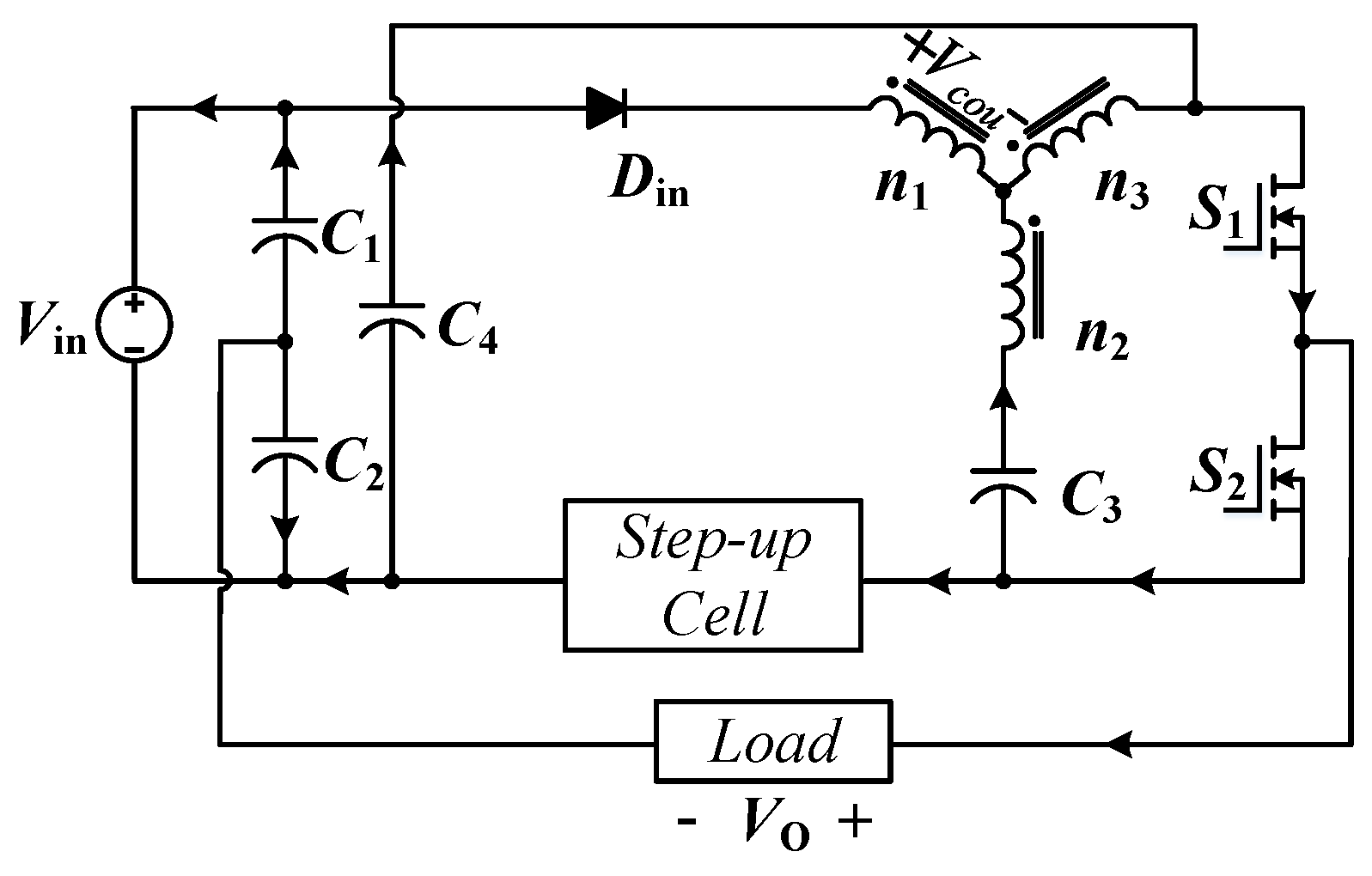
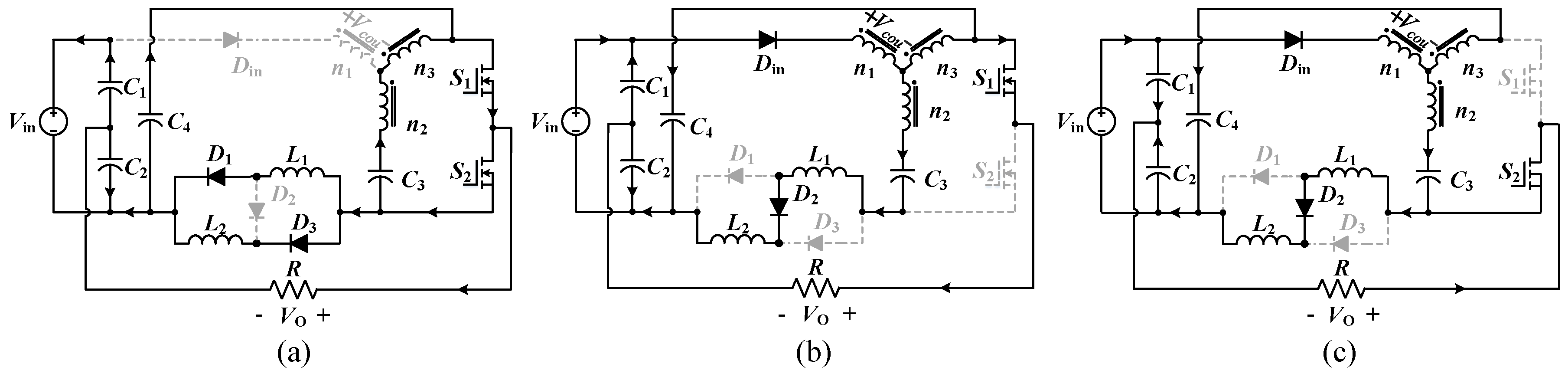
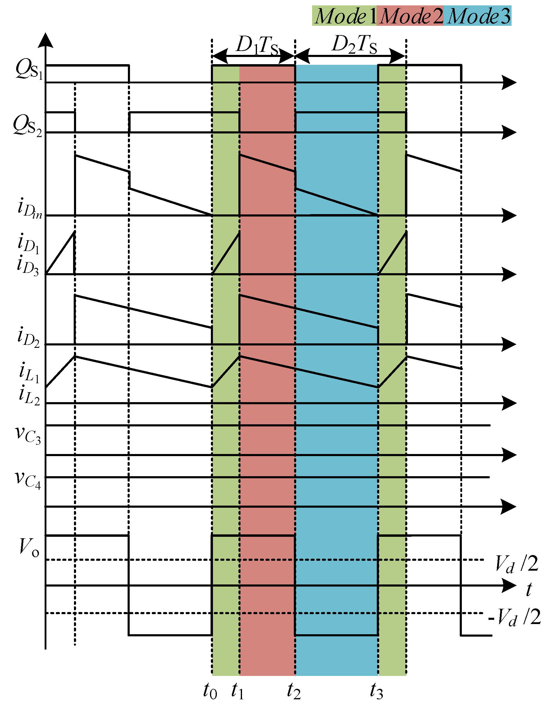
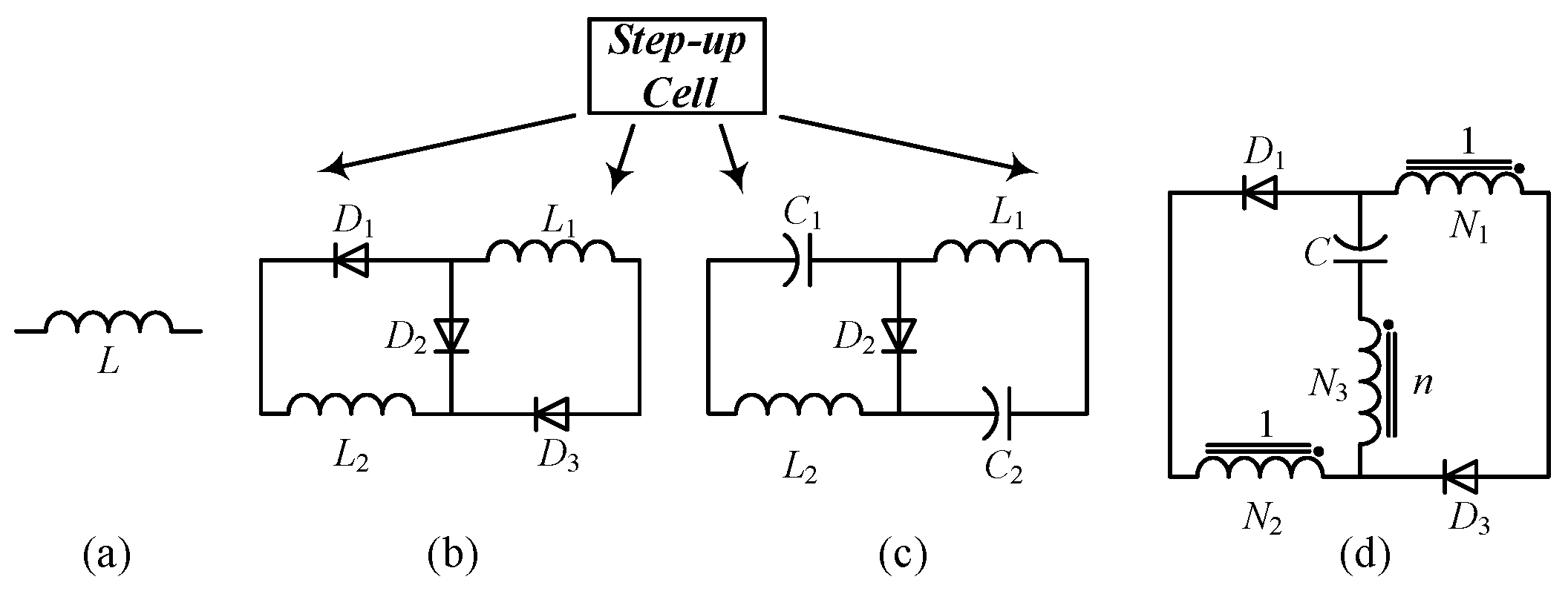
2. Operating Principle and Analysis

The structure of the proposed topologies are depicted in Figure 1 and the step-up cells are illustrated in Figure 2, in which the step-up cell is a general cell, which can be a single inductor, a switched inductor, a quasi Z-source network, or a switched-coupled inductor [19]. The cell endows the proposed converters with an additional voltage adjustment function.
Since the operating principles of the proposed converters are the same as the conventional ones with the condition of D 1 + D 2 1 , but not D 1 + D 2 > 1 , the latter is analyzed in this study. Furthermore, different step-up cells perform the same boost function, so a switched inductor Y-impedance-network half-bridge converter is analyzed as a typical example. In detail, a Y-impedance-network and a switched inductor are integrated into a conventional half-bridge inverter to form a new topology with three operating modes, as shown in Figure 3.
Denote t 0 as the beginning of one period, t 1 as the turning point from Mode 1 to Mode 2, t 2 as the time from Mode 2 to Mode 3, and t 3 = T S as the end of the period. The operating process in one period is analyzed in detail in the following, and the output voltage v o is deduced in each mode.
(1) Mode 1: t [ t 0 , t 1 ] .
As shown in Figure 3a, the proposed converter works in a shoot-through state. Diodes D in and D 2 are reverse biased simultaneously, capacitors C 3 discharges energy to the coupled inductor, and capacitors C 4 and the input voltage source discharge energy to the switched inductor cell ( L 1 , L 2 ) and the load R. Voltages across inductors L 1 , L 2 , coupled inductor n 1 , and output voltage can be deduced as
v L 1 = v L 2 = v C 4 ,
v n 1 = n 12 n 13 n 12 n 13 v C 3 ,
and
v o = v L 1 v C 2 = v C 4 v C 2 ,
where n 12 = n 1 / n 2 and n 13 = n 1 / n 3 are turns ratios of the three-winding coupled inductor.
(2) Mode 2: t [ t 1 , t 2 ] .
As shown in Figure 3b, switch S 1 is on and S 2 is off. Diodes D 1 and D 3 are reverse biased while D in and D 2 conduct at time t 1 . The input power V in begins to transfer energy to the Y-impedance-network and recharge C 3 , and the energy of L 1 and L 2 is delivered to C 2 , C 4 , and the load. The output voltage is the same as (3). Furthermore, the voltages across inductors L 1 , L 2 , and the coupled inductor n 1 are deduced as
v L 1 = v L 2 = V in v C 3 1 + n 12 n 12 v n 1 2 ,
and
v n 1 = 1 + n 13 n 13 ( V in v C 4 ) .
(3) Mode 3: t [ t 2 , t 3 ] .
As shown in Figure 3c, switch S 1 is off and S 2 is on. Similar to Mode 2, D 1 and D 3 are reverse biased while D in and D 2 conduct at time t 2 . The voltage of inductors L 1 , L 2 , and the coupled inductor n 1 are same as (4) and (5), respectively. The energy that capacitor C 2 and the switched inductor cell ( L 1 , L 2 ) release to the resistive load and output voltage can be deduced as
v o = 2 v L 1 v C 2 .
In terms of voltage-second property in L 1 ( L 2 ) and n 1 , one can obtain
0 T S v L 1 d t = 0
and
0 T S v n 1 d t = 0 .
By substitutig (1) and (4) into (7), we can deduce that
( D 1 + D 2 1 ) T S · V C 4 + ( 2 D 1 D 2 ) T S · ( V in V C 3 1 + n 12 n 12 v n 1 2 ) = 0 ,
where D 1 and D 2 are duty cycles of switches S 1 and S 2 , respectively.
Substitute (2) and (5) into (8), and we can deduce that
( D 1 + D 2 1 ) T S · n 12 n 13 n 12 n 13 · V C 3 + ( 2 D 1 D 2 ) T S · n 13 1 + n 13 · ( V in V C 4 ) = 0 .
One can obtain the voltages of C 3 and C 4 , i.e., V C 3 and V C 4 , via the solution of (9) and (10). Similarly, in terms of ampere second property in capacitor C 2 , one can obtain
0 T S i C 2 d t = 0 ,
where i C 2 is the current flowing through C 2 .
Denote the errors of v C 1 and v C 2 as Δ v C 1 and Δ v C 2 , respectively. As shown in Figure 3, we can obtain that v C 1 + v C 2 = V in , Δ v C 1 = Δ v C 2 and i o = i C 1 i C 2 . Therefore, it can be deduced that i C 1 = i C 2 = i o / 2 on the basis of i = C d u / d t , and (11) can be derived as
( V C 4 V C 2 ) 2 R L D 1 T S + ( V in V C 2 V C 3 n 23 ( 1 + n 12 ) 1 + n 13 ( V in V C 4 ) ) 2 R ( 1 D 1 ) · T S = 0 ,
where n 23 = n 2 / n 3 and R is the resistive load.
Thus, the output voltage V o can be deduced as
V o = V in ( 1 D 1 ) ( D 1 + D 2 ) 2 + ( K 1 ) ( D 1 + D 2 ) K ( D 1 + D 2 ) 2 , when S 1 is on , V in D 1 ( D 1 + D 2 ) 2 + ( K 1 ) ( D 1 + D 2 ) K ( D 1 + D 2 ) 2 , when S 1 is off and S 2 is on ,
where K = ( 1 + n 13 ) / ( 1 n 23 ) = ( n 1 + n 3 ) / ( n 3 n 2 ) .
According to (13), it is noted that positive output voltage is equal to negative only if D 1 = 0.5 . By adjusting the duty ratio of the switches and the winding ratio of the coupled inductors, we can obtain asymmetric and symmetric voltages, and positive and negative peak output voltages. When v o / V d < 1 , the proposed converter performs as a buck converter; when v o / V d > 1 , it functions as a boost converter. Therefore, it acts as a buck-boost converter.
In the same way, the output voltages of the inductor Y-impedance-network, quasi-Z-source, and switched-coupled-inductor Y-impedance-network are summarized in Table 1, in which D 1 = 0.5 and D = D 1 + D 2 .
The key waveforms of the proposed converter are depicted in Figure 4, where Q S 1 and Q S 2 stand for the driving voltages of switches S 1 and S 2 , respectively; i D in , i D 1 , and i D 2 are the currents across diodes D in , D 1 , and D 2 , respectively; i L 1 and i L 2 are the currents across inductors L 1 and L 2 , respectively; v C 1 and v C 2 are the voltages of capacitors C 1 , C 2 , respectively; and v o is the output voltage. As shown in Figure 4, it is obvious that the output voltage of the proposed converter exceeds the limited output voltages of the traditional half-bridge converter which are V in / 2 and V in / 2 .

3. Voltage Gain Analysis

In order to demonstrate the characteristics of the proposed converter, a performance comparison of the conventional Z-source half-bridge converter and the proposed converter is presented in this section.
The authors in [7] proposed a topology that implements a Z-source impedance network into a half-bridge inverter. The Z-source half-bridge converter not only solved the conventional problems, but also the problem of imbalance at the midpoint of the voltage of input capacitors. However, the Z-source half-bridge converter achieves a limited voltage gain, so it can no longer satisfy the high-voltage-gain requirement of BIPV.
Compared to the above topology, a Y-impedance-network takes the place of the Z-source network in the proposed converter. Under the premise of solving the above problems, the proposed topology has a higher boosting capacity owing to the existence of the Y-impedance-network. The winding factors are shown in Figure 5, which illustrate that with a large duty cycle and K value comes a large voltage gain, and as shown, the voltage gain can be several times higher than that of the conventional one.

4. Simulation Verifications

To verify the feasibility and validity of the proposed converter, PSIM software was applied for the simulation.
The preassigned parameters are as listed as follows: input voltage V in = 10 V, resistive load R = 200 Ω , permitted fluctuation range x C = 1%, x L = 10%, and period T S = 100 μ s. The high harmonic frequency of the capacitance and inductance are approximately equal to the switching frequency of the converter. Therefore, d v C , d i L and d t can be deduced as
d v C = x C V C ,
d i L = x L I L ,
and
d t ( D 1 + D 2 1 ) T S .
Thus, capacitors and inductors are designed as
L = v L d t d i L = v L ( D 1 + D 2 1 ) T S x L I L ,
and
C = i C d t d v C = i C ( D 1 + D 2 1 ) T S x C V C .
Then, based on the analysis in Section 2, the parameters can be expressed as
L 1 = L 2 = V C 4 ( D 1 + D 2 1 ) T S 2 x L I L , L m = n 1 n 3 n 2 · V C 3 ( 1 D 2 ) T S 2 x L I L , C 1 = C 2 = I o ( D 1 + D 2 1 ) T S 2 x C V C 1 , C 3 = I n 3 ( D 1 + D 2 1 ) T S x C V C 3 , C 4 = ( I o + 2 I L ) ( D 1 + D 2 1 ) T S x C V C 4 .
Therefore, the parameters of the converter are chosen as follows: L m = 470 μ H, n 1 : n 2 : n 3 = 5:1:3, C 1 = C 2 = 47 μ F, C 3 = C 4 = 470 μ F, and L 1 = L 2 = 420 μ H.
Simulations are shown in Figure 6, and the output voltage of the proposed converter V o 60 V, which is consistent with the theoretical analyses, is shown in Figure 4. Under the same conditions, as documented in [7], the voltage gain of the conventional converter can be calculated as 0.735 and the output voltage V o 7.35 V, which coincides with the simulations in Figure 6b. As shown in Figure 6, by adjusting the turns ratio and duty cycle, the voltage gain of the proposed converter can be eight times higher than that of the conventional.

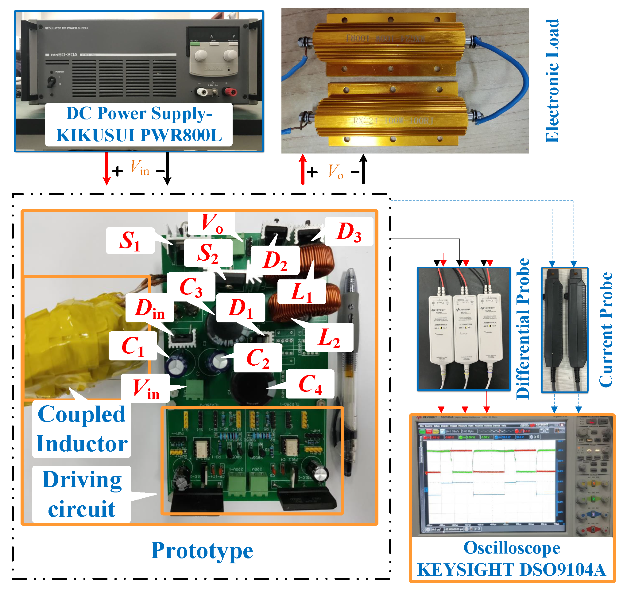
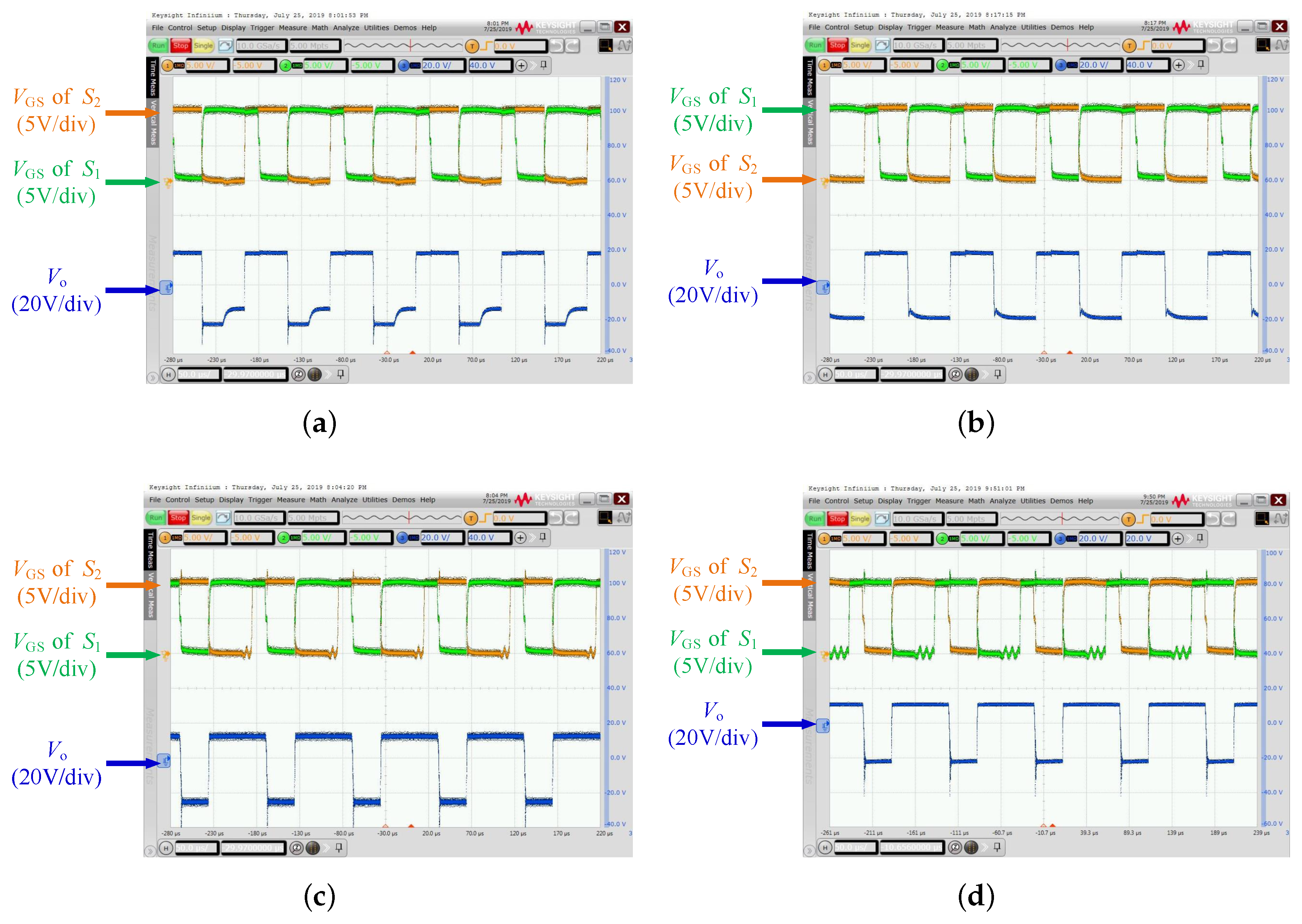
5. Experimental Verifications

In this section, the experimental environment and physical prototype are established, which are shown in Table 2 and Figure 7, to verify the theoretical analyses. Experimental parameters are shown in Table 3.
The experimental results are shown in Figure 8, which contains gate-source voltages of switches V GS 1 , V GS 2 , the output voltage V o . It is noted that the experimental results agree well with the theoretical analyses and simulation, demonstrating the functionality and feasibility of the proposed converter.
In order to demonstrate the practicality and implementability of the proposed converter comprehensively, key waveforms of the proposed converter with different turns ratios and duty ratios are shown in Figure 9. Therein, with small inductance of the coupled inductor, the proposed converter operates in discontinuous conduction mode (DCM), as shown in Figure 9a,b. When D 1 0.5 , the negative and positive output voltages are asymmetric, as shown in Figure 9c,d, which agrees well with above theoretically analyses.

6. Conclusions

In this study, a novel buck-boost half-bridge converter is proposed, which combines a Y-impedance-network and a family of step-up cells with a conventional half-bridge inverter to realize the additional voltage adjustment function. The simulation and experimental results show that by adjusting the turns ratio and duty cycle, they can achieve a high voltage gain which satisfies the high-voltage-gain requirement of BIPV, something which conventional inverters cannot achieve. In detail, the proposed Y-impedance-network-based half-bridge converter without additional step-up cells can realize 10 times the voltage adjustment function of traditional half-bridge converters. With additional step-up cells, the voltage adjustment range is enlarged, which also verifies the wide voltage adjustment functions of the proposed idea. Furthermore, the proposed converters can output symmetric or asymmetric positive and negative voltages, which validates its applicability and implementability for industrial applications. Therefore, the proposed solution in this paper can offer a potential voltage adjustment method in various industrial applications.

Author Contributions

Conceptualization, G.Z.; methodology, G.Z., S.C., Y.Z.; software, H.C.; validation, H.C.; formal analysis, H.C.; investigation, G.Z., S.C., Y.Z., L.Q.; writing–original draft preparation, H.C.; writing–review and editing, G.Z.; supervision, G.Z., L.Q.; project administration, Y.Z., L.Q.; funding acquisition, L.Q., Y.Z.

Funding

This research was funded by [National Natural Science Foundation of China] grant numbers [51907032, U1501251, 51277030, 61733015], [Natural Science Foundation of Guangdong Province] grant numbers [2017A030310243, 2018A030313365] and [Science and Technology Planning Project of Guangzhou] grant number [201804010310].

Conflicts of Interest

The authors declare no conflict of interest. The funders had no role in the design of the study; in the collection, analyses, or interpretation of data; in the writing of the manuscript, or in the decision to publish the results.

Abbreviations

The following abbreviations are used in this manuscript:
BIPVBuilding Integrated Photovoltaic
ZSIZ-source inverter
DCMdiscontinuous conduction mode
qZSIquasi-Z-source inverter

References

  1. Raugei, M.; Frankl, P. Life cycle impacts and costs of photovoltaic systems: Current state of the art and future outlooks. Energy 2009, 34, 392–399. [Google Scholar] [CrossRef]
  2. Xue, Y.; Chang, L.; Kjaer, S.B.; Bordonau, J.; Shimizu, T. Topologies of single-phase inverters for small distributed power generators: An overview. IEEE Trans. Power Electron. 2004, 19, 1305–1314. [Google Scholar] [CrossRef]
  3. Debnath, D.; Chatterjee, K. Solar photovoltaic-based stand-alone scheme incorporating a new boost inverter. IET Power Electron. 2016, 9, 621–630. [Google Scholar] [CrossRef]
  4. Asl, E.S.; Babaei, E.; Sabahi, M.; Nozadian, M.H.B.; Cecati, C. New half-bridge and full-bridge topologies for a switched-boost inverter with continuous input current. IEEE Trans. Ind. Electron. 2018, 65, 3188–3197. [Google Scholar] [CrossRef]
  5. Kim, B.; Kim, S.; Huh, D.Y.; Choi, J.H.; Kim, M. Hybrid resonant half-bridge DC/DC converter with wide input voltage range. In Proceedings of the 2018 IEEE Applied Power Electronics Conference and Exposition (APEC), San Antonio, TX, USA, 4–8 March 2018. [Google Scholar]
  6. Peng, F.Z. Z-source inverter. IEEE Trans. Ind. Appl. 2003, 39, 504–510. [Google Scholar] [CrossRef]
  7. Zhang, G.; Li, Z.; Zhang, B.; Qiu, D.; Xiao, W.; Halang, W.A. A Z-Source Half-Bridge Converter. IEEE Trans. Ind. Electron. 2013, 61, 1269–1279. [Google Scholar] [CrossRef]
  8. Strzelecki, R.; Adamowicz, M.; Strzelecka, N.; Bury, W. New type T-source inverter. In Proceedings of the 2009 Compatibility and Power Electronics, Badajoz, Spain, 20–22 May 2009. [Google Scholar]
  9. Kumar, S.P.; Shailaja, P. T-shaped Z-source inverter. Int. J. Eng. Res. Technol. 2012, 1, 1–6. [Google Scholar]
  10. Qian, W.; Peng, F.Z.; Cha, H. Trans-Z-Source inverters. IEEE Trans. Power Electron. 2003, 26, 3453–3463. [Google Scholar] [CrossRef]
  11. Loh, P.C.; Li, D.; Blaabjerg, F. Γ-Z-source inverters. IEEE Trans. Power Electron. 2013, 28, 4880–4884. [Google Scholar] [CrossRef]
  12. Loh, P.C.; Blaabjerg, F. Magnetically coupled impedance-source inverters. IEEE Trans. Ind. Appl. 2013, 49, 2177–2187. [Google Scholar] [CrossRef]
  13. Siwakoti, Y.P.; Blaabjerg, F.; Galigekere, V.P.; Ayachit, A.; Kazimierczuk, M.K. A-source impedance network. IEEE Trans. Power Electron. 2016, 31, 8081–8087. [Google Scholar] [CrossRef]
  14. Siwakoti, Y.P.; Loh, P.C.; Blaabjerg, F.; Town, G. Y-source impedance network. IEEE Trans. Power Electron. 2014, 29, 3250–3254. [Google Scholar] [CrossRef]
  15. Asghari-Gorji, S.; Mostaan, A.; Javadi, H. A new structure of Y-source inverters with continous input current and high voltage gain. In Proceedings of the 6th Power Electronics, Drive Systems & Technologies Conference (PEDSTC2015), Tehran, Iran, 3–4 February 2015. [Google Scholar]
  16. Siwakoti, Y.P.; Blaabjerg, F.; Loh, P.C. Quasi-Y-source inverter. In Proceedings of the 2015 Australasian Universities Power Engineering Conference (AUPEC), Wollongong, Australia, 27–30 September 2015. [Google Scholar]
  17. Liu, H.; Li, Y.; Liu, K.; Loh, P.C.; Wang, W.; Xu, D.; Blaabjerg, F. Extended quasi-Y-source inverter with suppressed inrush and leakage effects. IET Power Electron. 2018, 12, 719–728. [Google Scholar] [CrossRef]
  18. Fang, X.; Ding, X.; Zhong, S.; Tian, Y. Improved quasi-Y-source DC-DC converter for renewable energy. CPSS Trans. Power Electron. Appl. 2019, 4, 163–170. [Google Scholar] [CrossRef]
  19. Ahmed, H.F.; Cha, H.; Kim, S.H.; Kim, H.G. Switched-coupled-inductor quasi-Z-source inverter. IEEE Trans. Power Electron. 2015, 31, 1241–1254. [Google Scholar] [CrossRef]
Figure 1. Proposed topology.
Energies 12 03430 g001
Figure 2. A step-up cell: (a) a single inductor; (b) switched inductor; (c) quasi Z-source network; (d) switched-coupled-inductor.
Energies 12 03430 g002
Figure 3. Equivalent circuits in (a) Mode 1: S 1 and S 2 are on; (b) Mode 2: S 1 is on and S 2 is off; (c) Mode 3: S 1 is off and S 2 is on.
Energies 12 03430 g003
Figure 4. Key waveforms of the switched inductor Y-impedance-network half-bridge converter.
Energies 12 03430 g004
Figure 5. The relationship between the voltage gain and duty cycle: winding factors.
Energies 12 03430 g005
Figure 6. Simulation waveforms when D 1 = 0.5 and D 2 = 0.66 of (a) proposed converter and (b) traditional converter in [7].
Energies 12 03430 g006
Figure 7. Prototypes with the experimental environment.
Energies 12 03430 g007
Figure 8. Experimental waveforms when the turns ratio is 5:1:3 and the duty ratio is D 1 = 0.5 , D 2 = 0.66 .
Energies 12 03430 g008
Figure 9. Experimental waveforms of the proposed converter in: (a) turns ratio 3:1:5, duty ratio D 1 = 0.5 , D 2 = 0.66 ; (b) turns ratio 1:3:5, duty ratio D 1 = 0.5 , D 2 = 0.66 ; (c) turns ratio 3:1:5, duty ratio D 1 = 0.66 , D 2 = 0.5 ; (d) turns ratio 1:3:5, duty ratio D 1 = 0.66 , D 2 = 0.5 .
Energies 12 03430 g009
Table 1. Output voltage and voltage gain of the proposed converters with different step-up cell.
Converters V o + V o Voltage Gain G
Inductor Y-impedance-network V in ( 1 D 1 ) 2 + K ( 1 + K ) ( D 1 + D 2 ) V in D 1 2 + K ( 1 + K ) ( D 1 + D 2 ) 1 2 ( 2 + K ( 1 + K ) D )
Switched inductor Y-impedance-network V in ( 1 D 1 ) ( D 1 + D 2 ) 2 + ( K 1 ) ( D 1 + D 2 ) K ( D 1 + D 2 ) 2 V in D 1 ( D 1 + D 2 ) 2 + ( K 1 ) ( D 1 + D 2 ) K ( D 1 + D 2 ) 2 D 2 ( 2 + ( K 1 ) D K D 2 )
Quasi Z-source Y-impedance-network V in ( 1 D 1 ) 3 + K ( K + 2 ) ( D 1 + D 2 ) V in D 1 3 + K ( K + 2 ) ( D 1 + D 2 ) 1 3 + K ( K + 2 ) D
Switched-coupled-inductor Y-impedance-network V in ( 1 D 1 ) 2 + ( n + 2 ) K ( 2 K + n K + 1 ) ( D 1 + D 2 ) V in D 1 2 + ( n + 2 ) K ( 2 K + n K + 1 ) ( D 1 + D 2 ) 1 2 ( 2 + ( n + 2 ) K ( 2 K + n K + 1 ) D )
Table 2. Experimental platform.
DC Power SupplyOscilloscopeVoltage ProbeCurrent Probe
KIKUSUI PWR800LAgilent DSO7104AKEYSIGHT N2843AAgilent 1147A
Table 3. Experimental Parameters.
ParametersValueParasitic Parameters
Input voltage V in 10 [V]
Output voltage V o 60 [V]
Switching frequency f s 10 [kHz]
Driving ICTLP250
MOSFET S 1 , S 2 IXTQ88N30P40 [m Ω ]
Inductors L 1 , L 2 420 [ μ H]200 [m Ω ]
Three winding-coupledMagnetizing inductance 470 [ μ H]
inductorTurns ratio 5:1:3 290 [m Ω ]: 260 [m Ω ]: 270 [m Ω ]
Diodes D 1 , D 2 , D 3 , D in MBRF20200CT1 [V] / 0.05 [m Ω ]
Capacitors C 1 , C 2 47 [ μ F]/100 [V]500 [m Ω ]
Capacitor C 3 , C 4 470 [ μ F]/250 [V]200 [m Ω ]
Resistive load200 [ Ω ]

