Zero Current Switching Switched-Capacitors Balancing Circuit for Energy Storage Cell Equalization and Its Associated Hybrid Circuit with Classical Buck-Boost


Abstract
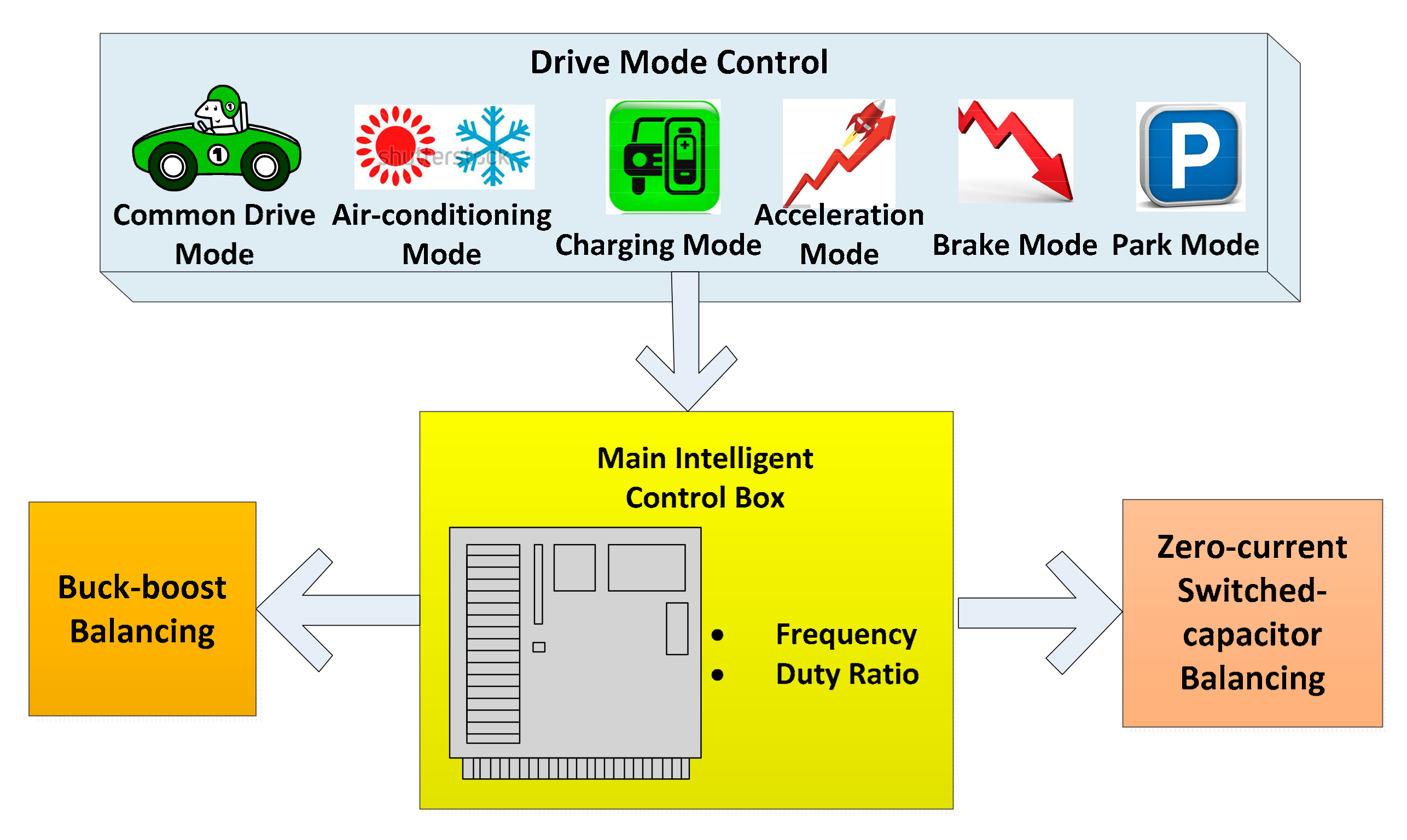
1. Introduction
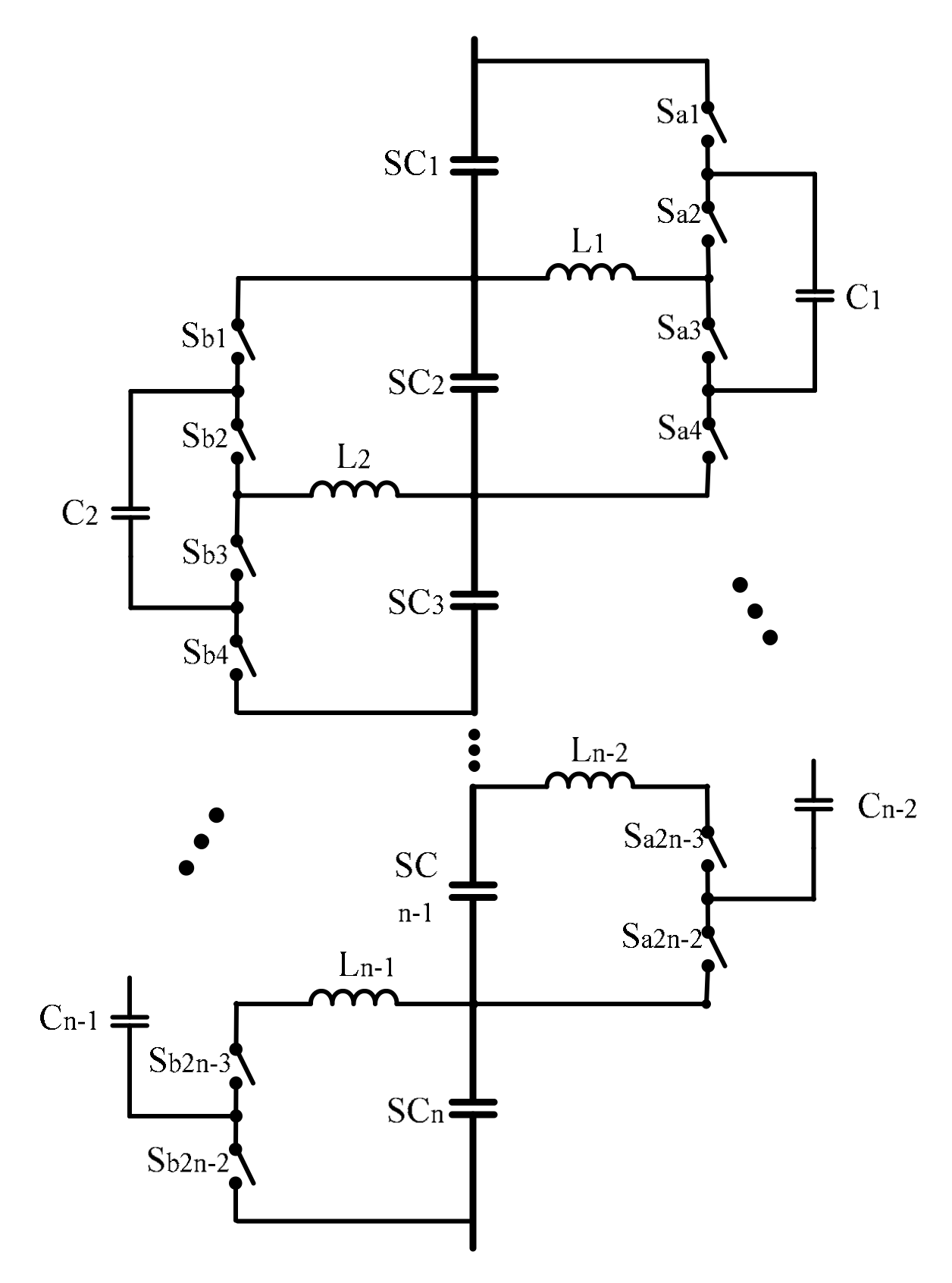
2. Proposed Cell Balancing Circuits
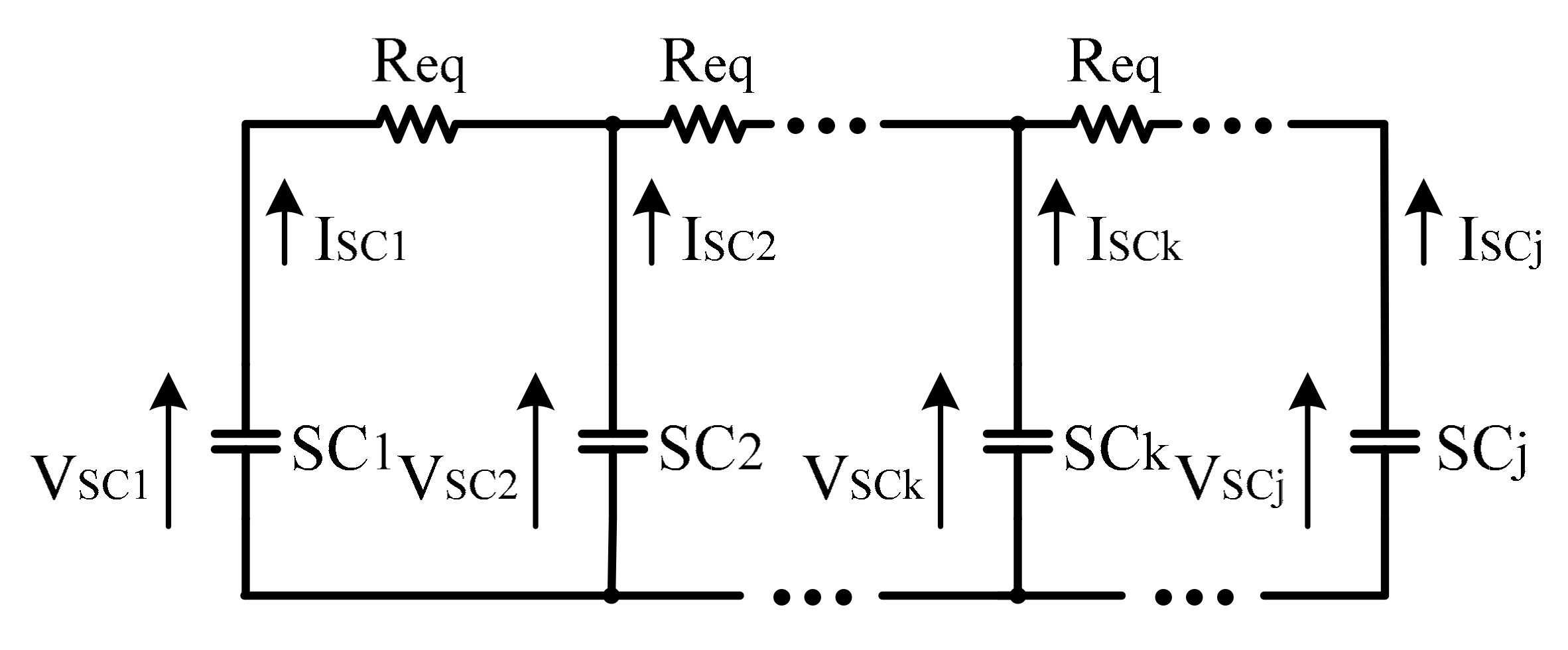
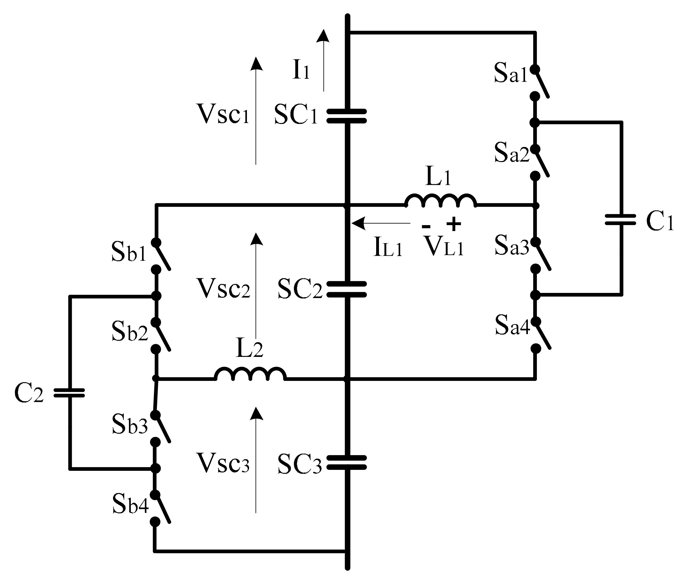
2.1. Circuit Configuration
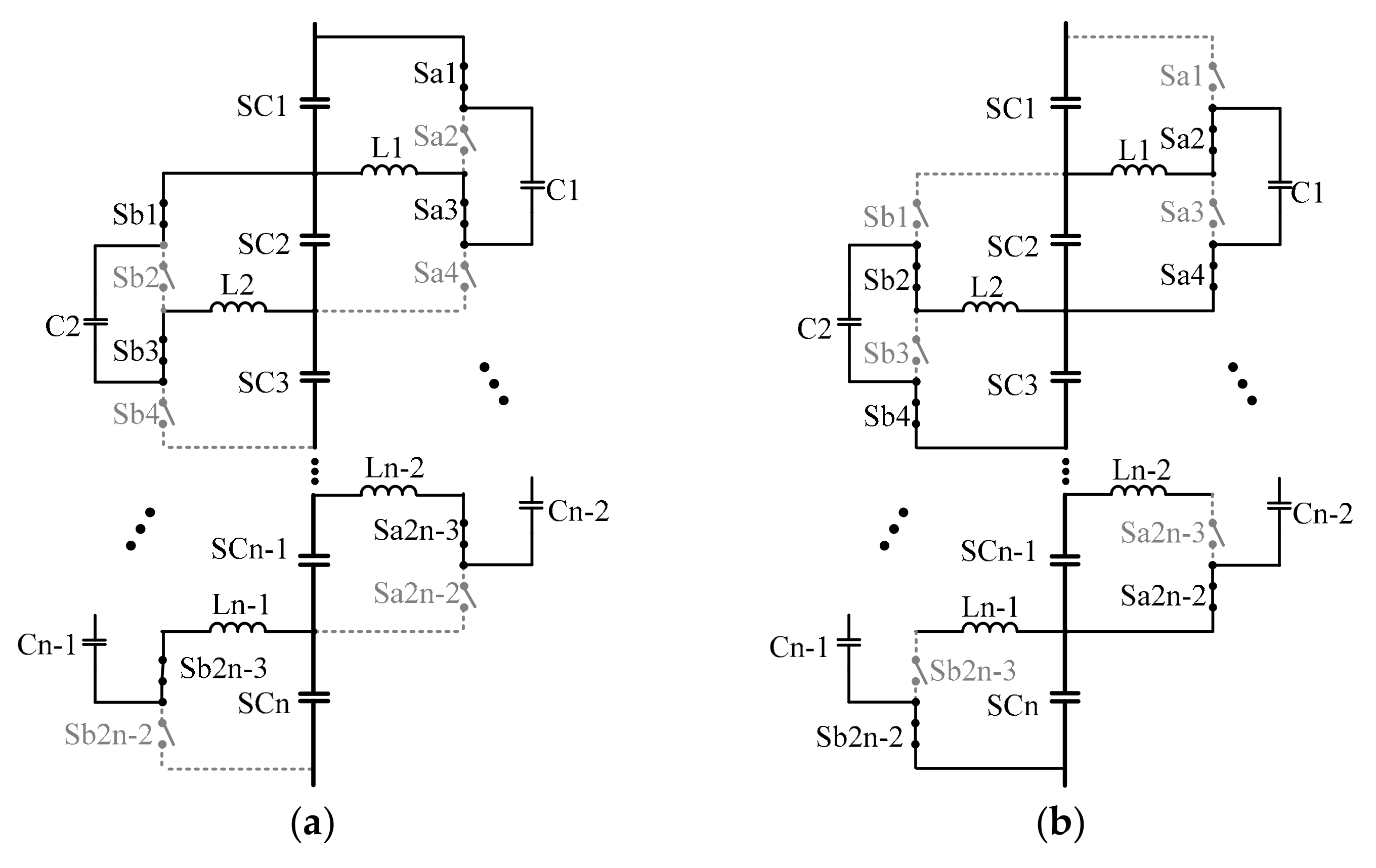
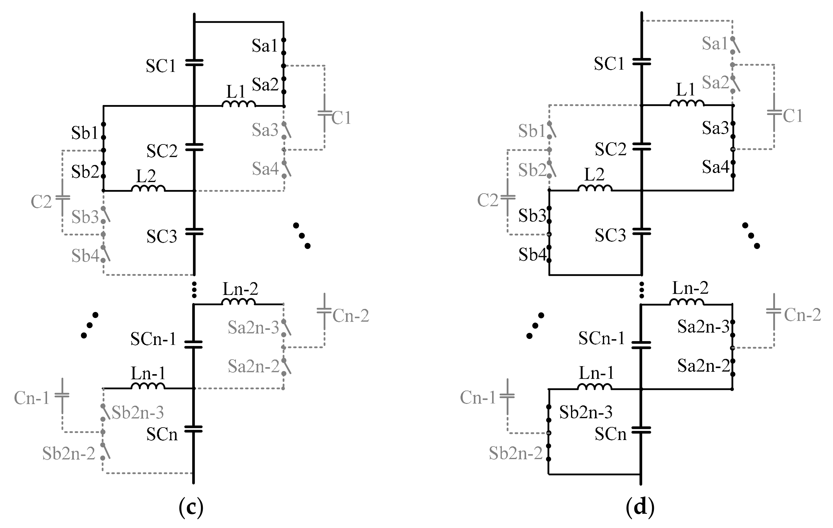
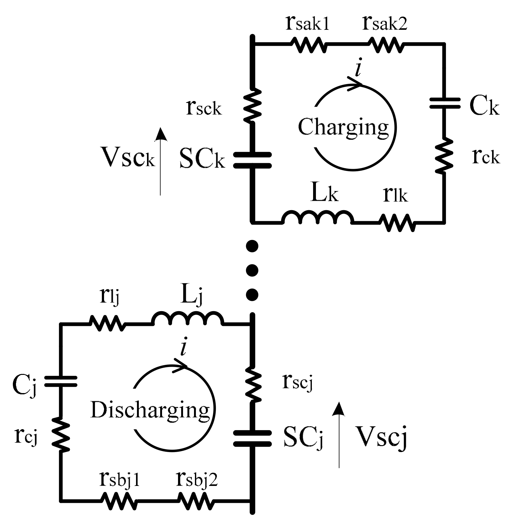
2.2. Balancing Circuit Operation Analysis
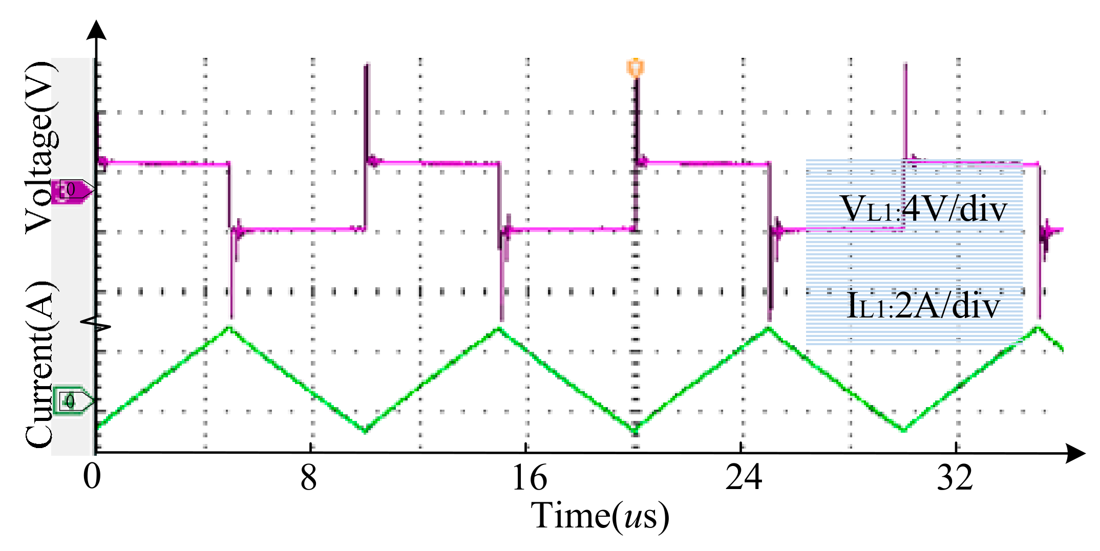
2.3. Analysis of ZCS Operation
3. Modeling for Balancing Mode
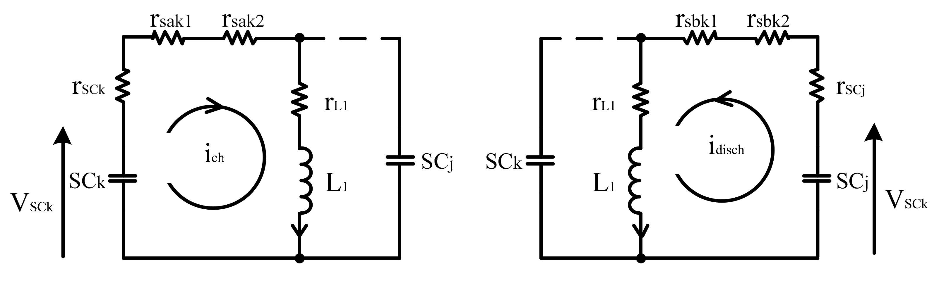
3.1. Modeling for ZCS Balancing Mode
3.2. Modeling for Buck-Boost Balancing Mode
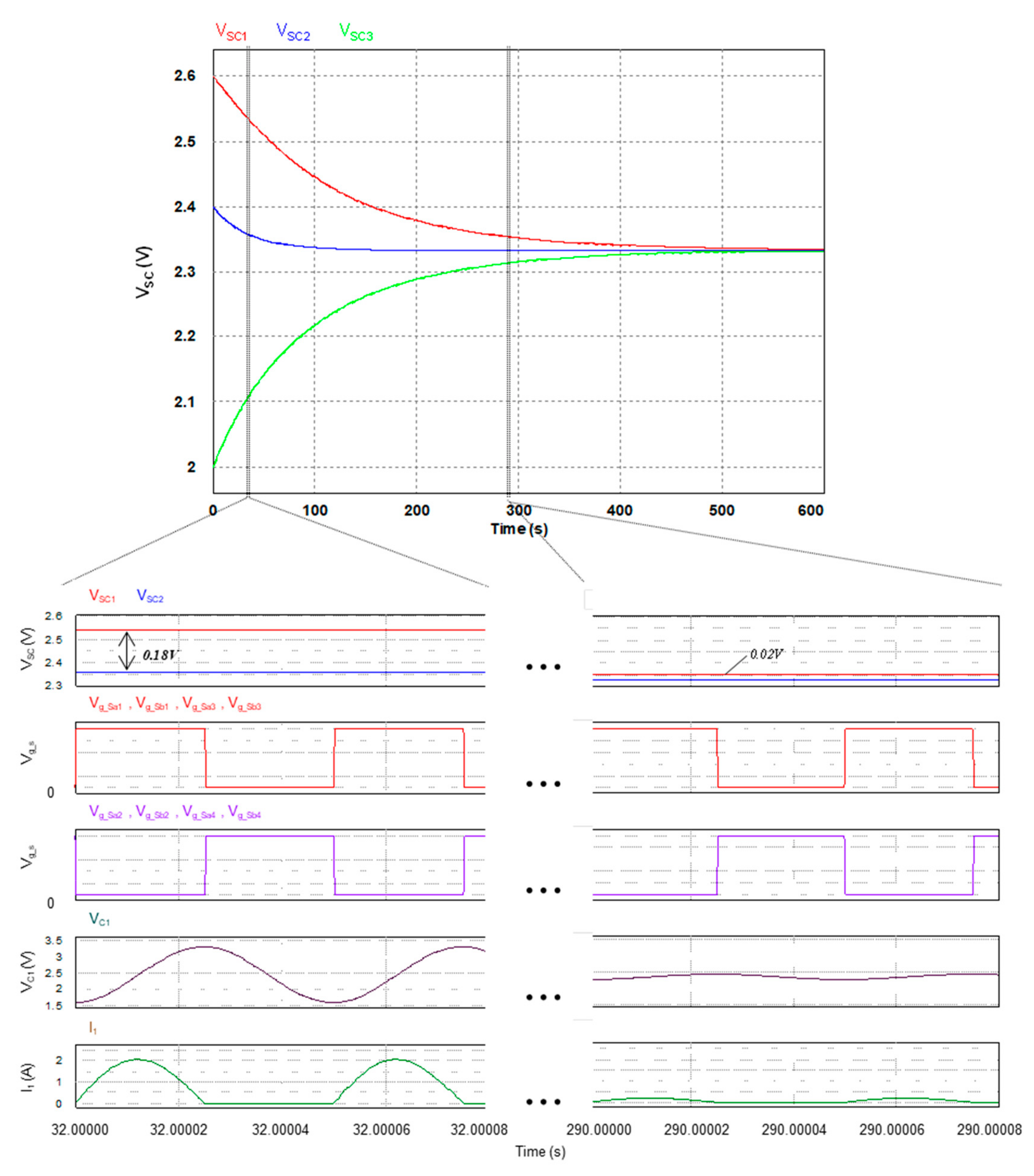
4. Simulation Results of the Multi-Function Voltage Equalizer
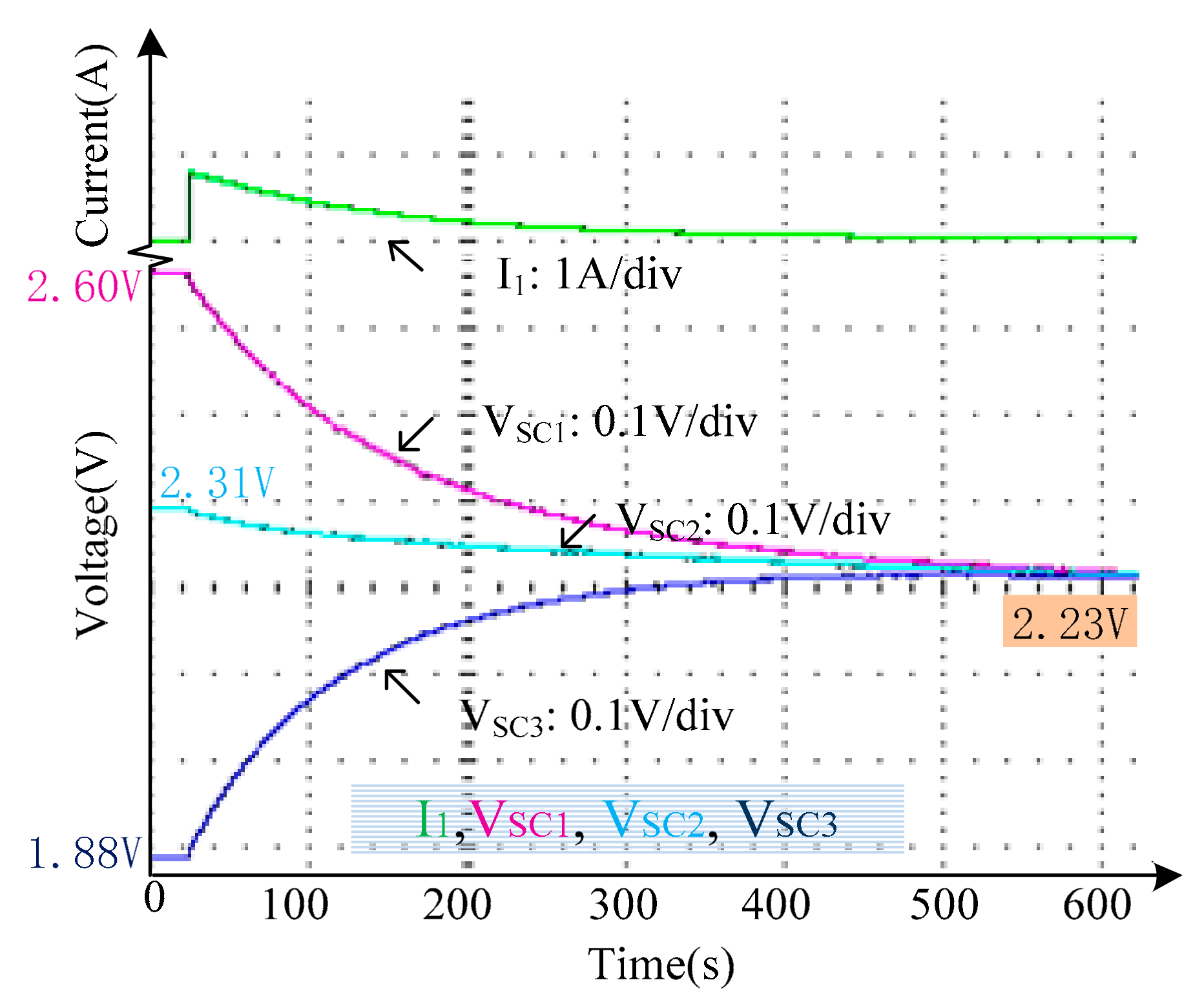
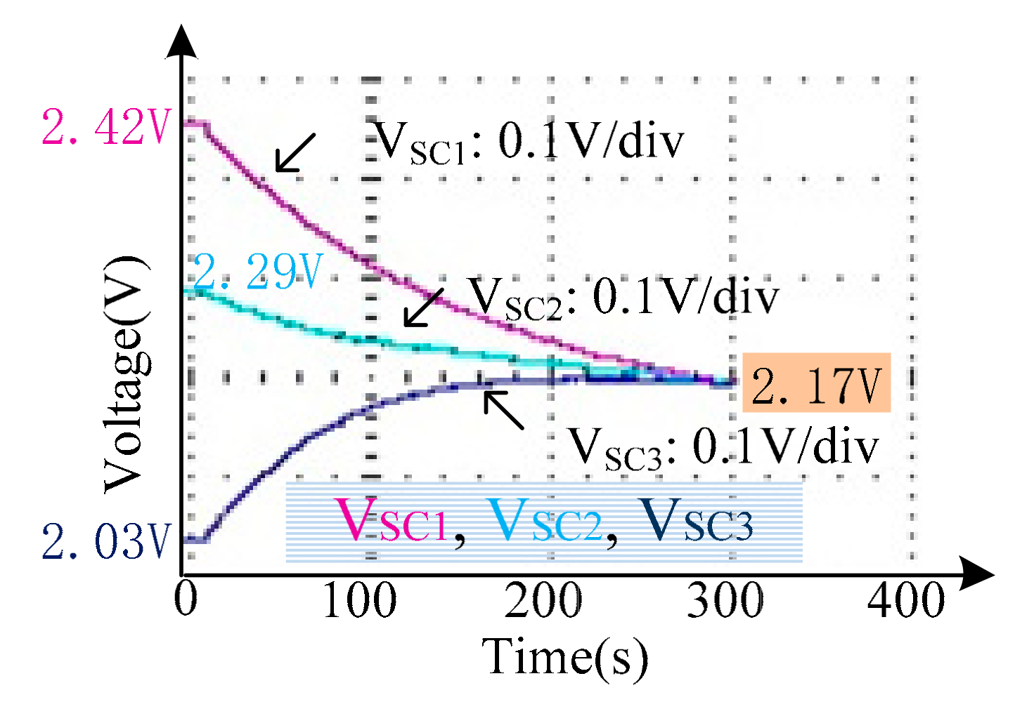
5. Experimental Results of the Multi-Function Circuit
6. Conclusions
Author Contributions
Funding
Acknowledgments
Conflicts of Interest
References
- Fotouhi, A.; Auger, D.J.; Propp, K.; Longo, S. Electric vehicle battery parameter identification and SOC observability analysis: NiMH and Li-S case studies. IET Power Electron. 2017, 10, 1289–1297. [Google Scholar] [CrossRef]
- Kandasamy, K.; Vilathgamuwa, D.M.; Madawala, U.K.; Tseng, K.-J. Inductively coupled modular battery system for electric vehicles. IET Power Electron. 2016, 9, 600–609. [Google Scholar] [CrossRef]
- Ju, F.; Deng, W.; Li, J. Performance Evaluation of Modularized Global Equalization System for Lithium-Ion Battery Packs. IEEE Trans. Automat. Sci. Eng. 2016, 13, 986–996. [Google Scholar] [CrossRef]
- Brando, G.; Dannier, A.; Spina, I.; Tricoli, P. Integrated BMS-MMC Balancing Technique Highlighted by a Novel Space-Vector Based Approach for BEVs Application. Energies 2017, 10, 1628. [Google Scholar] [CrossRef]
- Guo, X.; Kang, L.; Huang, Z.; Yao, Y.; Yang, H. Research on a Novel Power Inductor-Based Bidirectional Lossless Equalization Circuit for Series-Connected Battery Packs. Energies 2015, 8, 5555–5576. [Google Scholar] [CrossRef]
- Ye, Y.; Cheng, K.W.E. An Automatic Switched-Capacitor Cell Balancing Circuit for Series-Connected Battery Strings. Energies 2016, 9, 138. [Google Scholar] [CrossRef]
- Xu, A.; Xie, S.; Liu, X. Dynamic voltage equalization for series connected ultracapacitors in EV/HEV applications. IEEE Trans. Veh. Technol. 2009, 58, 3981–3987. [Google Scholar]
- Choudhury, A.; Pillay, P.; Williamson, S.S. Comparative Analysis Between Two-Level and Three-Level DC/AC Electric Vehicle Traction Inverters Using a Novel DC-Link Voltage Balancing Algorithm. IEEE J. Emerg. Sel. Top. Power Electron. 2014, 2, 529–540. [Google Scholar] [CrossRef]
- Shili, S.; Hijazi, A.; Sari, A.; Lin-Shi, X.; Venet, P. Balancing circuit new control for supercapacitor storage system lifetime maximization. IEEE Trans. Power Electron. 2017, 32, 4939–4948. [Google Scholar] [CrossRef]
- Chemali, E.; Preindl, M.; Malysz, P.; Emadi, A. Electrochemical and Electrostatic Energy Storage and Management Systems for Electric Drive Vehicles: State-of-the-Art Review and Future Trends. IEEE J. Emerg. Sel. Top. Power Electron. 2016, 4, 1117–1134. [Google Scholar] [CrossRef]
- Cheng, K.W.E.; Divakar, B.P.; Wu, H.; Ding, K.; Ho, H.F. Battery-Management System (BMS) and SOC Development for Electrical Vehicles. IEEE Trans. Veh. Technol. 2011, 60, 76–88. [Google Scholar] [CrossRef]
- Cao, J.; Schofield, N.; Emadi, A. Battery balancing methods: A comprehensive review. In Proceedings of the IEEE Vehicle Power and Propulsion Conference, Harbin, China, 3–5 September 2008; pp. 1–6. [Google Scholar]
- Shang, Y.; Zhang, C.; Cui, N.; Guerrero, J.M. A Cell-to-Cell Battery Equalizer with Zero-Current Switching and Zero-Voltage Gap Based on Quasi-Resonant LC Converter and Boost Converter. IEEE Trans. Power Electron. 2015, 30, 3731–3747. [Google Scholar] [CrossRef]
- Lee, Y.-S.; Cheng, M.-W. Intelligent Control Battery Equalization for Series Connected Lithium-Ion Battery Strings. IEEE Trans. Ind. Electron. 2015, 52, 1297–1307. [Google Scholar] [CrossRef]
- Ye, Y.; Cheng, K.W.E.; Liu, J.; Ding, K. A Step-Up Switched-Capacitor Multilevel Inverter with Self-Voltage Balancing. IEEE Trans. Ind. Electron. 2014, 61, 6672–6680. [Google Scholar] [CrossRef]
- Ragheb, A.N.; Kim, H.W. Reference-Free Dynamic Voltage Scaler Based on Swapping Switched-Capacitors. Energies 2019, 12, 625. [Google Scholar] [CrossRef]
- Khodaparast, A.; Azimi, E.; Azimi, A.; Adabi, M.E.; Adabi, J.; Pouresmaeil, E. A New Modular Multilevel Inverter Based on Step-Up Switched-Capacitor Modules. Energies 2019, 12, 524. [Google Scholar] [CrossRef]
- Rodič, M.; Milanovič, M.; Truntič, M.; Ošlaj, B. Switched-Capacitor Boost Converter for Low Power Energy Harvesting Applications. Energies 2018, 11, 3156. [Google Scholar] [CrossRef]
- Wang, X.; Eric Cheng, K.W.; Fong, Y.C. Non-equal voltage cell balancing for Battery and super-capacitor management system using coupled inductor techniques. Energies 2018, 11, 1037. [Google Scholar] [CrossRef]
- Wang, X.; Eric Cheng, K.W.; Fong, Y.C. Series-Parallel Switched-Capacitor Balancing Circuit for Hybrid Source Package. IEEE Access 2018, 6, 34254–34261. [Google Scholar] [CrossRef]
- Pascual, C.; Krein, P.T. Switched capacitor system for automatic series battery equalization. In Proceedings of the APEC 97—Applied Power Electronics Conference, Atlanta, GA, USA, 27 February 1997; pp. 848–854. [Google Scholar]
- Baughman, A.C.; Ferdowsi, M. Double-tiered switched-capacitor battery charge equalization technique. IEEE Trans. Ind. Electron. 2008, 55, 2277–2285. [Google Scholar] [CrossRef]
- Kim, M.-Y.; Kim, C.-H.; Kim, J.-H.; Moon, G.-W. A chain structure of switched capacitor for improve cell balancing speed of lithium-ion batteries. IEEE Trans. Ind. Electron. 2014, 61, 3989–3999. [Google Scholar] [CrossRef]
- Cheng, K.W.E.; Evans, P.D. Parallel-mode extended-period quasiresonant convertor. IEE Proc. B 1991, 138, 243–251. [Google Scholar] [CrossRef]
- Hui, S.Y.R.; Cheng, K.W.E.; Prakash, S.R.N. A fully soft-switched extended-period quasi-resonant power-factor-correction circuit. IEEE Trans. Power Electron. 1997, 12, 922–930. [Google Scholar] [CrossRef]
- Jabbar, M.; Tehrani, U.D. Double-boost switched-resonator converter. IET Power Electron. 2018, 11, 1382–1388. [Google Scholar] [CrossRef]
- Lin, J.Y.; Lin, Y.F.; Lee, S.Y. A Novel Multi-Element Resonant Converter with Self-Driven Synchronous Rectification. Energies 2019, 12, 715. [Google Scholar] [CrossRef]
- Fong, Y.C.; Cheng, K.W.E.; Raman, S.R.; Wang, X. Multi-Port Zero-Current Switching Switched-Capacitor Converters for Battery Management Applications. Energies 2018, 11, 1934. [Google Scholar] [CrossRef]
- Wang, C.S.; Li, W.; Meng, Z.; Wang, Y.F.; Zhou, J.G. Three-Phase High-Power and Zero-Current-Switching OBC for Plug-In Electric Vehicles. Energies 2015, 8, 6672–6704. [Google Scholar] [CrossRef]
- Kutkut, N.H.; Wiegman, H.L.N.; Divan, D.M.; Novotny, D.W. Design considerations for charge equalization of an electric vehicle battery system. IEEE Trans. Ind. Electron. 1999, 35, 28–35. [Google Scholar] [CrossRef]
- Ohno, T.; Suzuki, T.; Koizumi, H. Modularized LC resonant switched capacitor cell voltage equalizer. In Proceedings of the IECON 2014—40th Annual Conference of the IEEE Industrial Electronics Society, Dallas, TX, USA, 29 October–1 November 2014; pp. 3156–3162. [Google Scholar]
- Lambert, S.M.; Pickert, V.; Atkinson, D.J.; Zhan, H. Transformer-Based Equalization Circuit Applied to n-Number of High Capacitance Cells. IEEE Trans. Power Electron. 2016, 31, 1334–1343. [Google Scholar] [CrossRef]
- Chen, Y.; Liu, X.; Cui, Y.; Zou, J.; Yang, S. A Multi-Winding Transformer Cell-to-Cell Active Equalization Method for Lithium-Ion Batteries With Reduced Number of Driving Circuits. IEEE Trans. Power Electron. 2016, 31, 4916–4929. [Google Scholar] [CrossRef]
- Ye, Y.M.; Eric Cheng, K.W. Quadratic boost converter with low buffer capacitor stress. IET Power Electron. 2014, 7, 1162–1170. [Google Scholar] [CrossRef]
- Ye, Y.M.; Cheng, K.W.E.; Liu, J.F.; Xu, C. A Family of Dual-Phase-Combined Zero-Current Switching Switched-Capacitor Converters. IEEE Trans Power Electron. 2014, 29, 4209–4218. [Google Scholar] [CrossRef]
- Zhang, Y.; Zhang, Y.; Ai, Z.; Feng, Y.; Cheng, W.; Hu, Z. Energy Saving Control Strategy for the High-Frequency Start-up Process for Electric Mining Haul Trucks. IEEE Trans. Intell. Veh. 2018, 3, 595–606. [Google Scholar] [CrossRef]
- Zhang, S.; Luo, Y.; Wang, J.; Wang, X.; Li, K. Predictive Energy Management Strategy for Fully Electric Vehicles Based on Preceding Vehicle Movement. IEEE Trans. Intell. Transp. Syst. 2017, 18, 3049–3060. [Google Scholar] [CrossRef]
- Rezaei, A.; Burl, J.B.; Rezaei, M.; Zhou, B. Catch Energy Saving Opportunity in Charge-Depletion Mode, a Real-Time Controller for Plug-In Hybrid Electric Vehicles. IEEE Trans. Veh. Technol. 2018, 67, 11234–11237. [Google Scholar] [CrossRef]
- Yuan, J.S.; Bi, Y. Process and temperature robust voltage multiplier design for RF energy harvesting. Microelectron. Reliab. 2014, 55, 107–113. [Google Scholar] [CrossRef]
- Yuan, J.S.; Xu, Y.; Yen, S.D.; Bi, Y.; Hwang, G.W. Hot carrier injection stress effect on a 65 nm lna at 70 ghz. IEEE Trans. Device Mater. Reliab. 2014, 14, 931–934. [Google Scholar] [CrossRef]


| Function Mode | Switching States | |||||||
|---|---|---|---|---|---|---|---|---|
| Sa2m−1 | Sa2m | Sa2m+1 | Sa2m+2 | Sb2m−1 | Sb2m | Sb2m+1 | Sb2m+2 | |
| ZCS mode | 1 | 0 | 1 | 0 | 1 | 0 | 1 | 0 |
| Buck boost mode | 1 | 1 | 0 | 0 | 1 | 1 | 0 | 0 |
| Mode | fs = 15 kHz | fs = 20 kHz | fs = 25 kHz |
| ZCS mode |  |  |  |
| X: Time (s); Y: Voltage (V) | |||
| fs = 15 kHz | fs = 20 kHz | fs = 25 kHz | |
 |  |  | |
| X: Time (s); Y: Current (A) | |||
| fs = 90 kHz | fs = 100 kHz | fs = 110 kHz | |
| Buck-boost mode |  |  |  |
| X: Time (s); Y: Voltage (V) | |||
| Units | Quantity |
|---|---|
| Supercapacitor (DRL357S0TQ60SC) | 3 |
| Capacitance of SCs | 350 F |
| MOSFET(IRFR3607PBF) 75 V 7.34 mΩ | 8 |
| ON-resistance of MOSFETs | 7.34 mΩ |
| Switched-capacitor (RNS1E220MDN1KX) | 2 |
| Capacitance of Switched-capacitors | 22 μF |
| ESR of Switched-capacitors | 28 mΩ |
| Inductor (WE-HCF) | 2 |
| Inductance of the inductor | 3.3 μH |
| ESR of Inductor | 1.31 mΩ |
| Switching frequency | 20 kHz, 100 kHz |
© 2019 by the authors. Licensee MDPI, Basel, Switzerland. This article is an open access article distributed under the terms and conditions of the Creative Commons Attribution (CC BY) license (http://creativecommons.org/licenses/by/4.0/).
Share and Cite
Wang, X.; Cheng, K.W.E.; Fong, Y.C. Zero Current Switching Switched-Capacitors Balancing Circuit for Energy Storage Cell Equalization and Its Associated Hybrid Circuit with Classical Buck-Boost. Energies 2019, 12, 2726. https://doi.org/10.3390/en12142726
Wang X, Cheng KWE, Fong YC. Zero Current Switching Switched-Capacitors Balancing Circuit for Energy Storage Cell Equalization and Its Associated Hybrid Circuit with Classical Buck-Boost. Energies. 2019; 12(14):2726. https://doi.org/10.3390/en12142726
Chicago/Turabian StyleWang, Xiaolin, Ka Wai Eric Cheng, and Yat Chi Fong. 2019. "Zero Current Switching Switched-Capacitors Balancing Circuit for Energy Storage Cell Equalization and Its Associated Hybrid Circuit with Classical Buck-Boost" Energies 12, no. 14: 2726. https://doi.org/10.3390/en12142726
APA StyleWang, X., Cheng, K. W. E., & Fong, Y. C. (2019). Zero Current Switching Switched-Capacitors Balancing Circuit for Energy Storage Cell Equalization and Its Associated Hybrid Circuit with Classical Buck-Boost. Energies, 12(14), 2726. https://doi.org/10.3390/en12142726