An LCC-P Compensated Wireless Power Transfer System with a Constant Current Output and Reduced Receiver Size


Abstract
1. Introduction
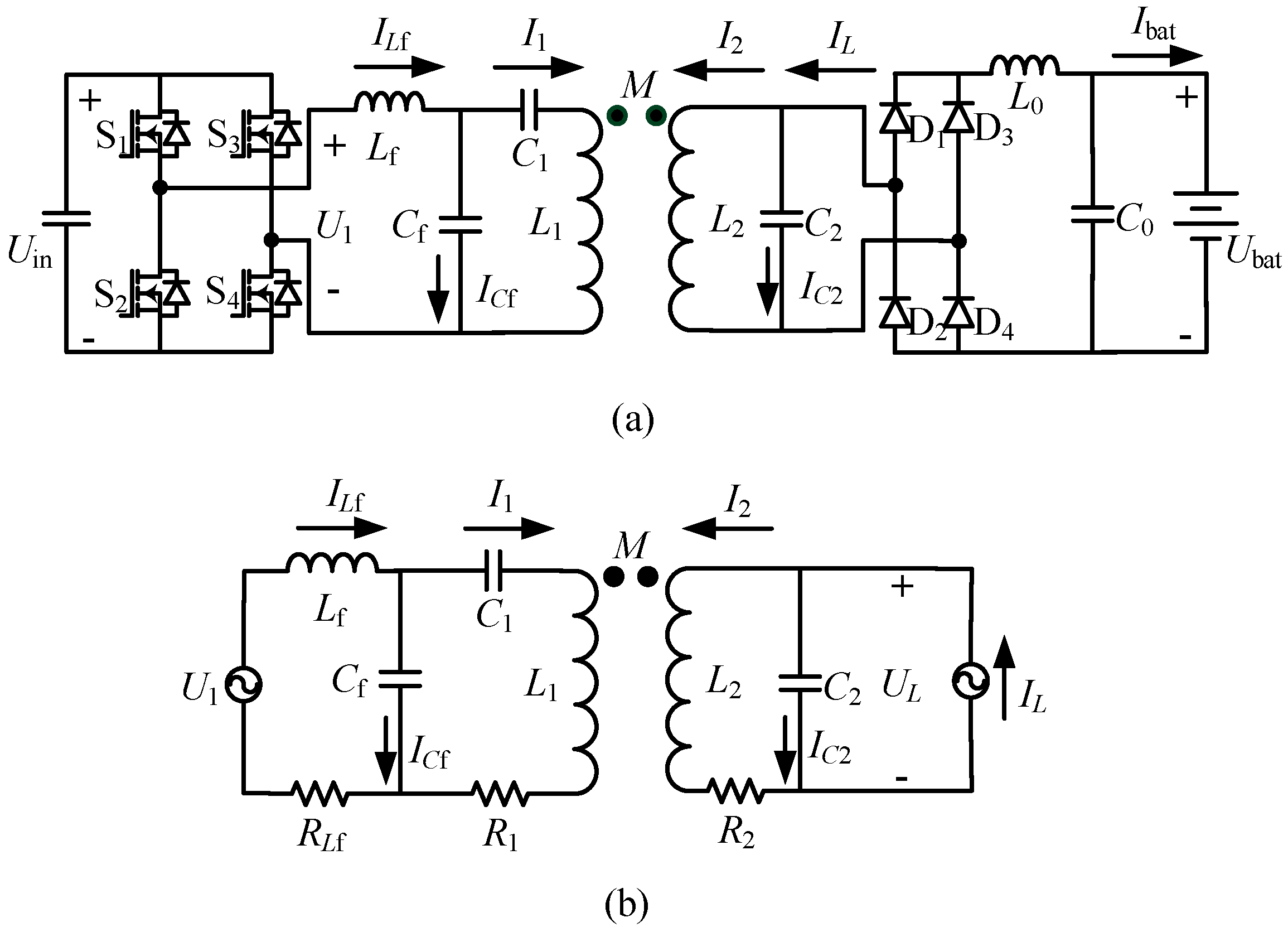
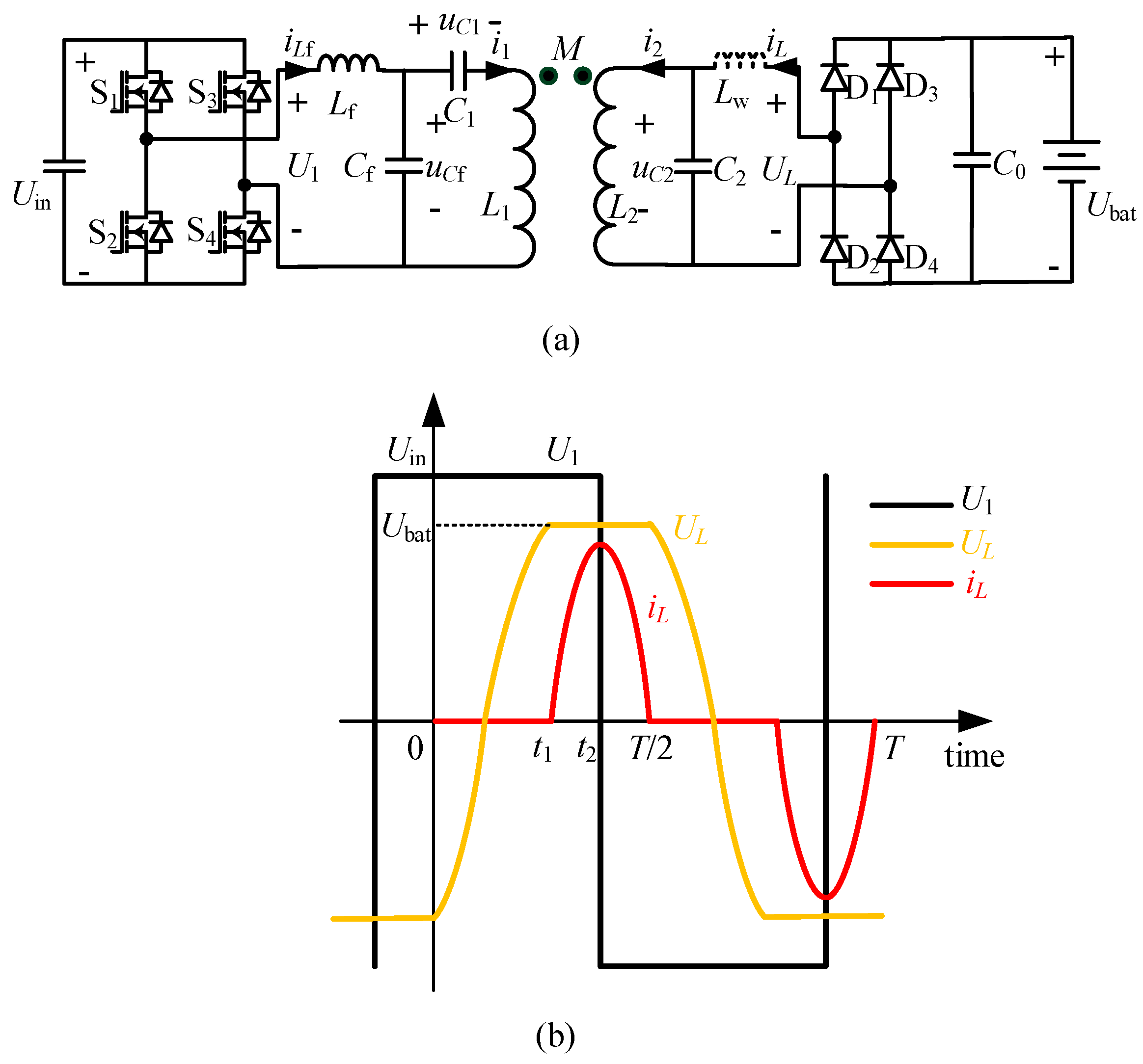
2. Circuit Analysis
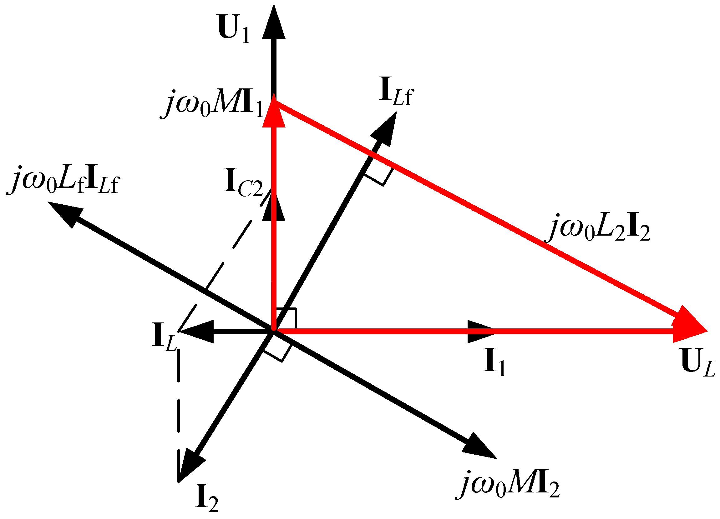
2.1. Theoretical Analysis
2.2. Eliminating L0
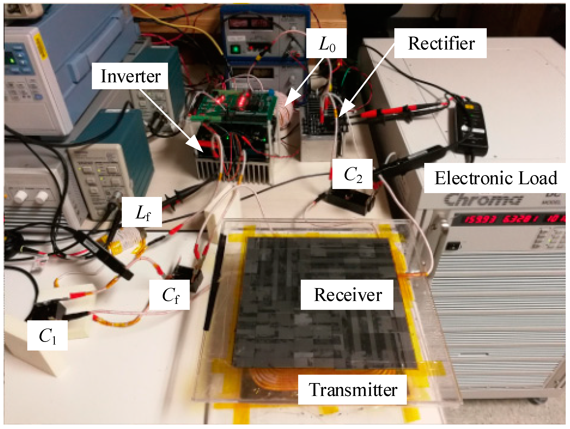
3. Calculations, Simulations, and Experiments
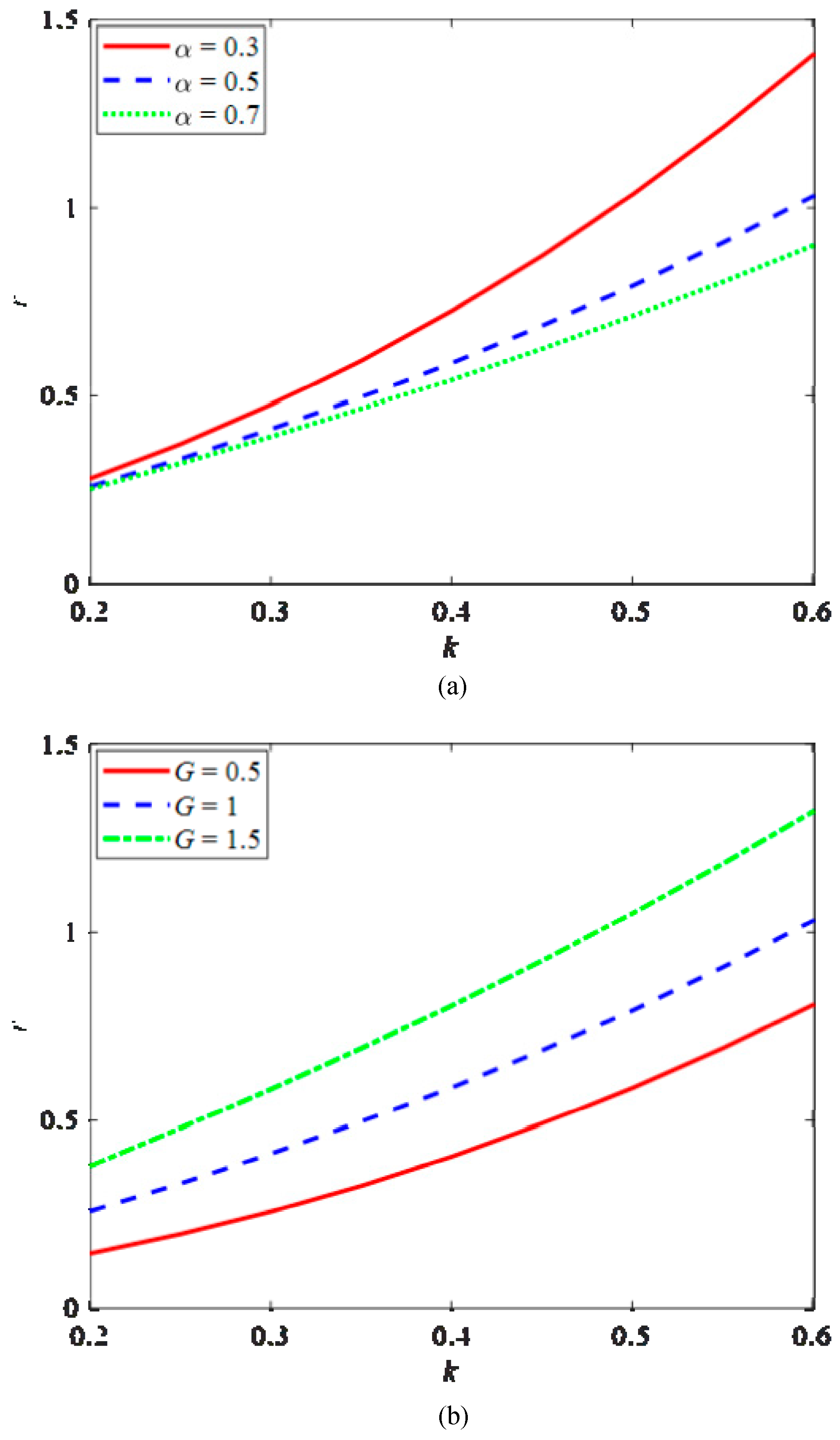
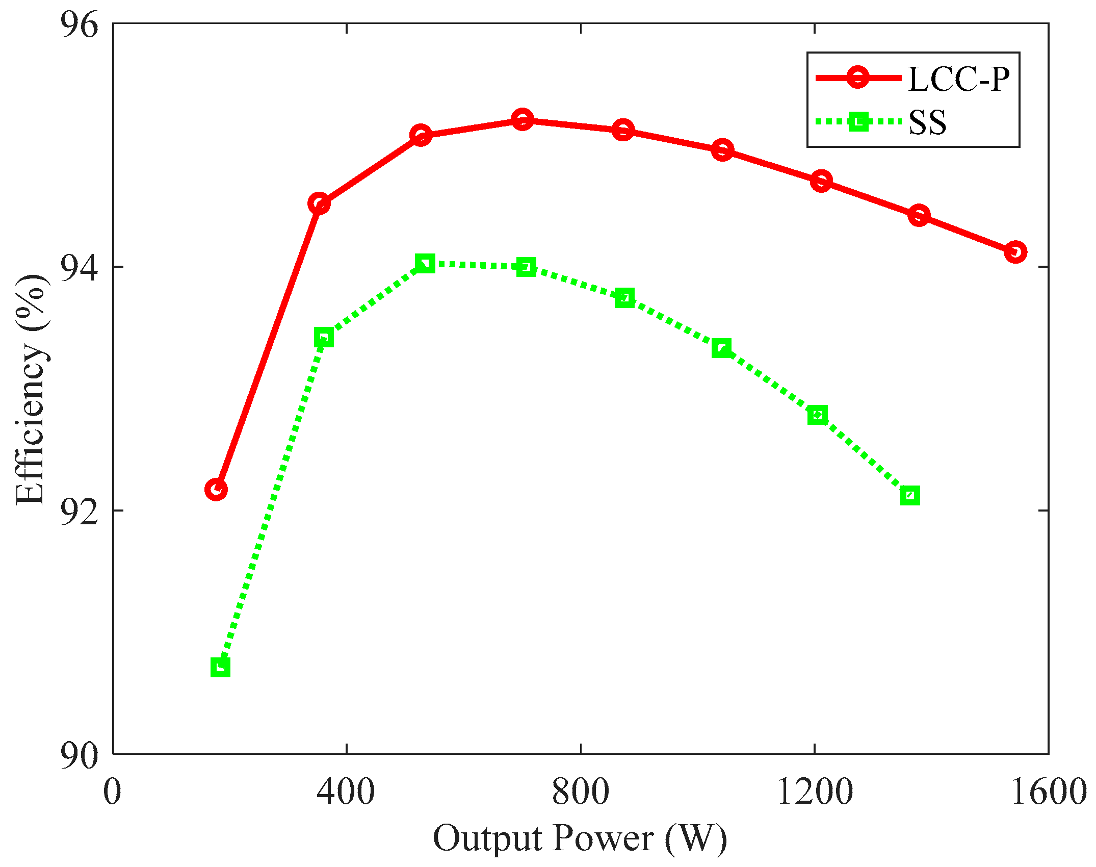
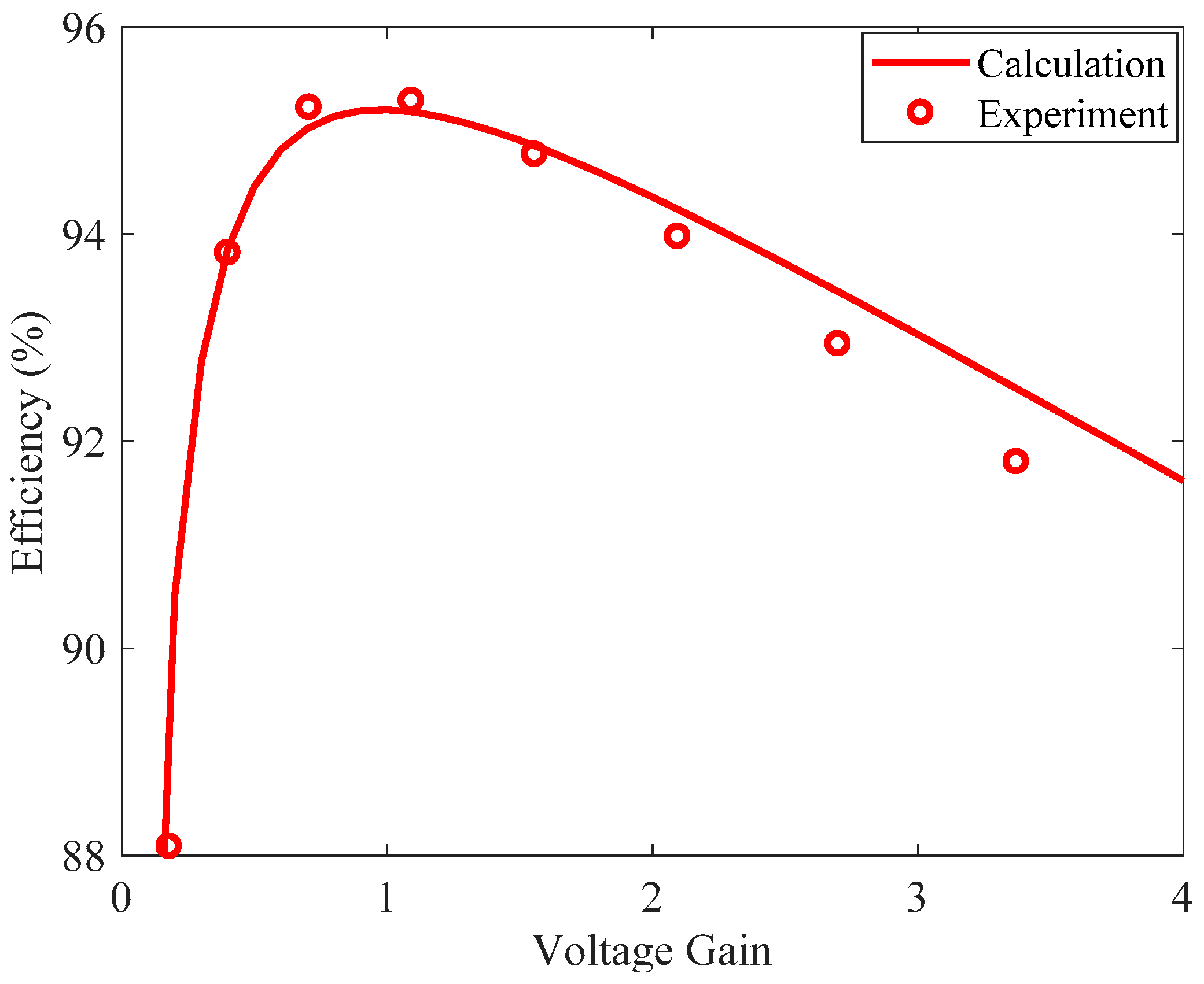
3.1. Comparison of LCC-P and SS Topology
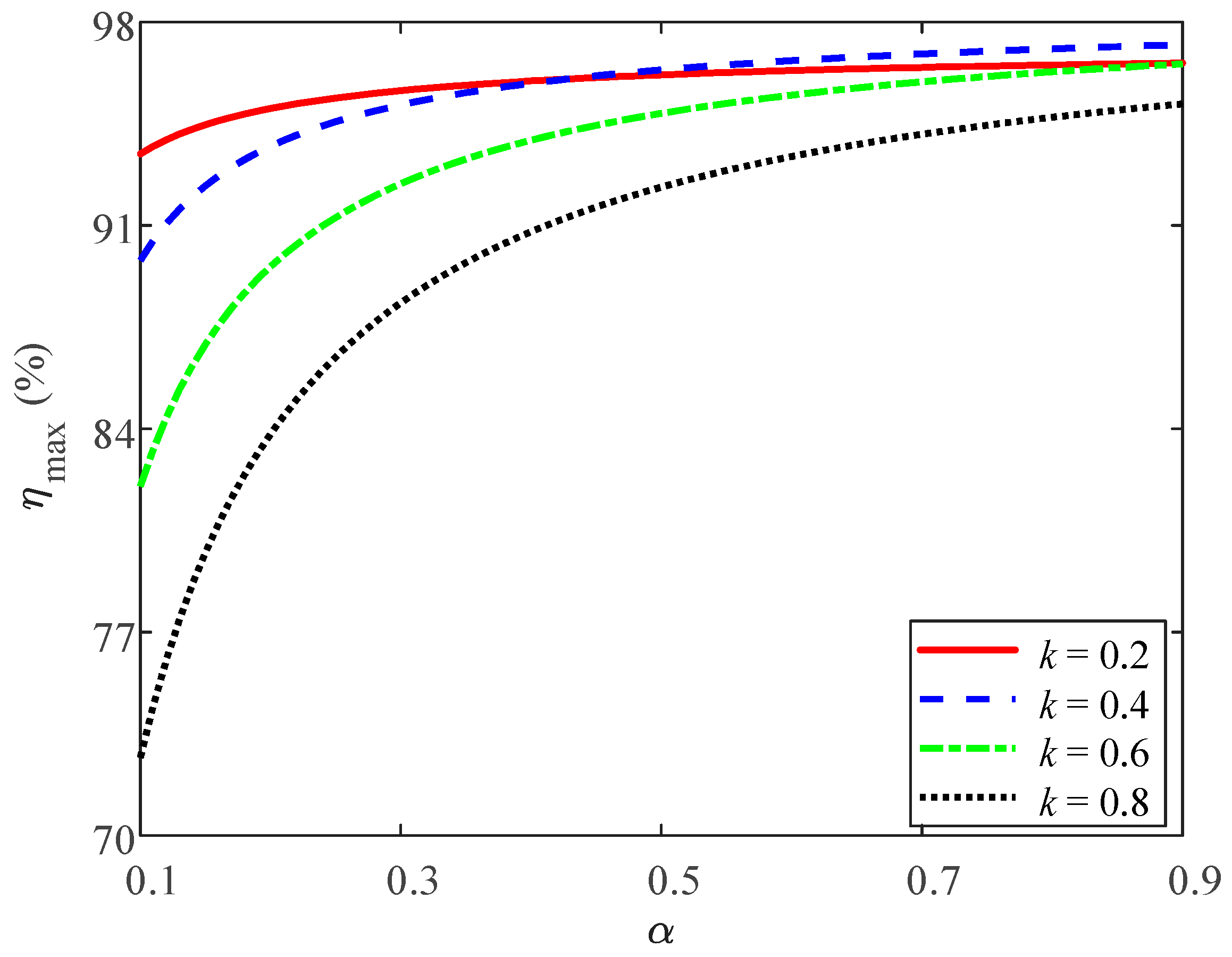
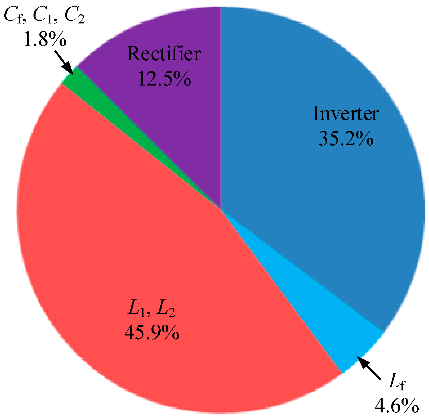
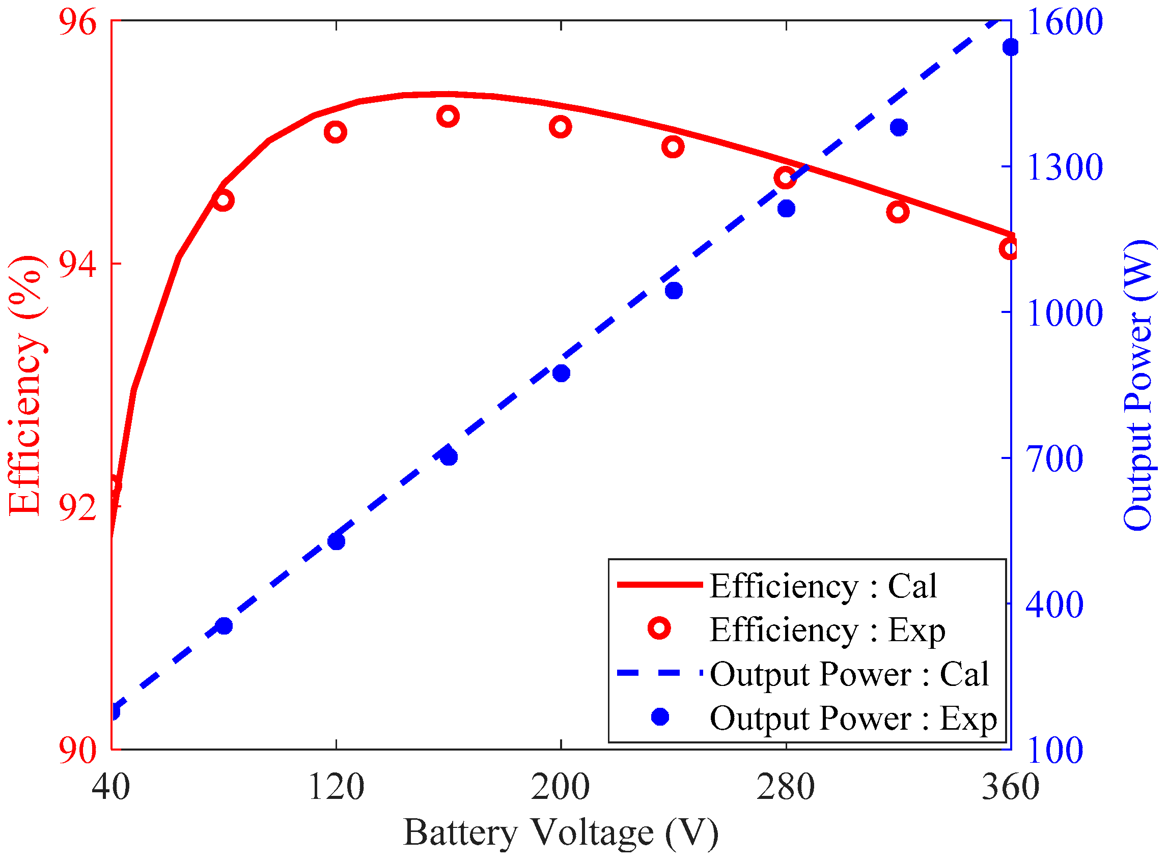
3.2. LCC-P Compensation Topology
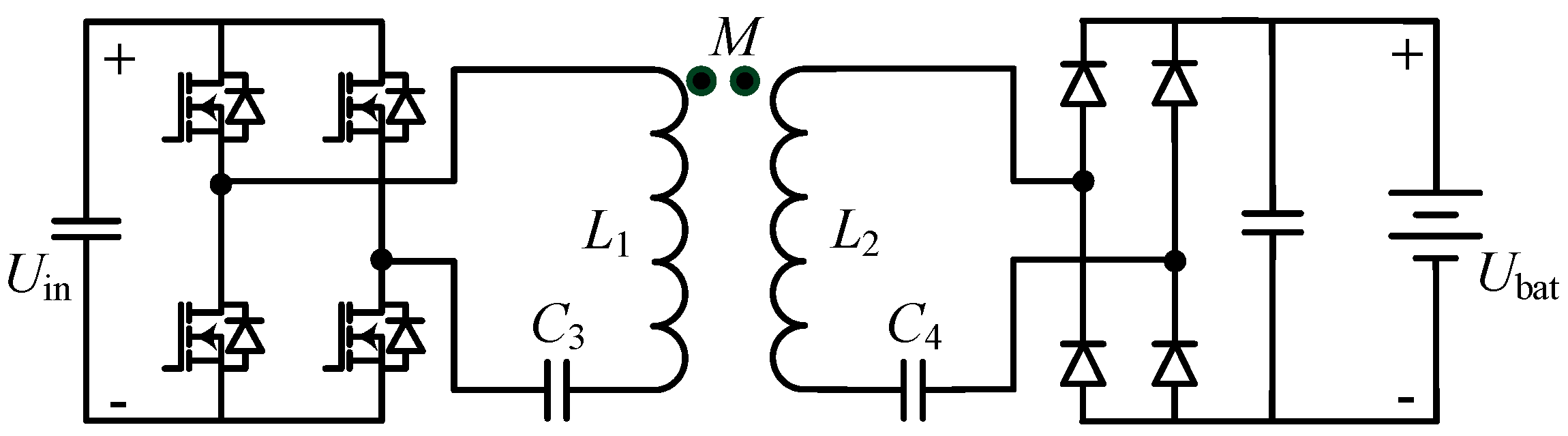
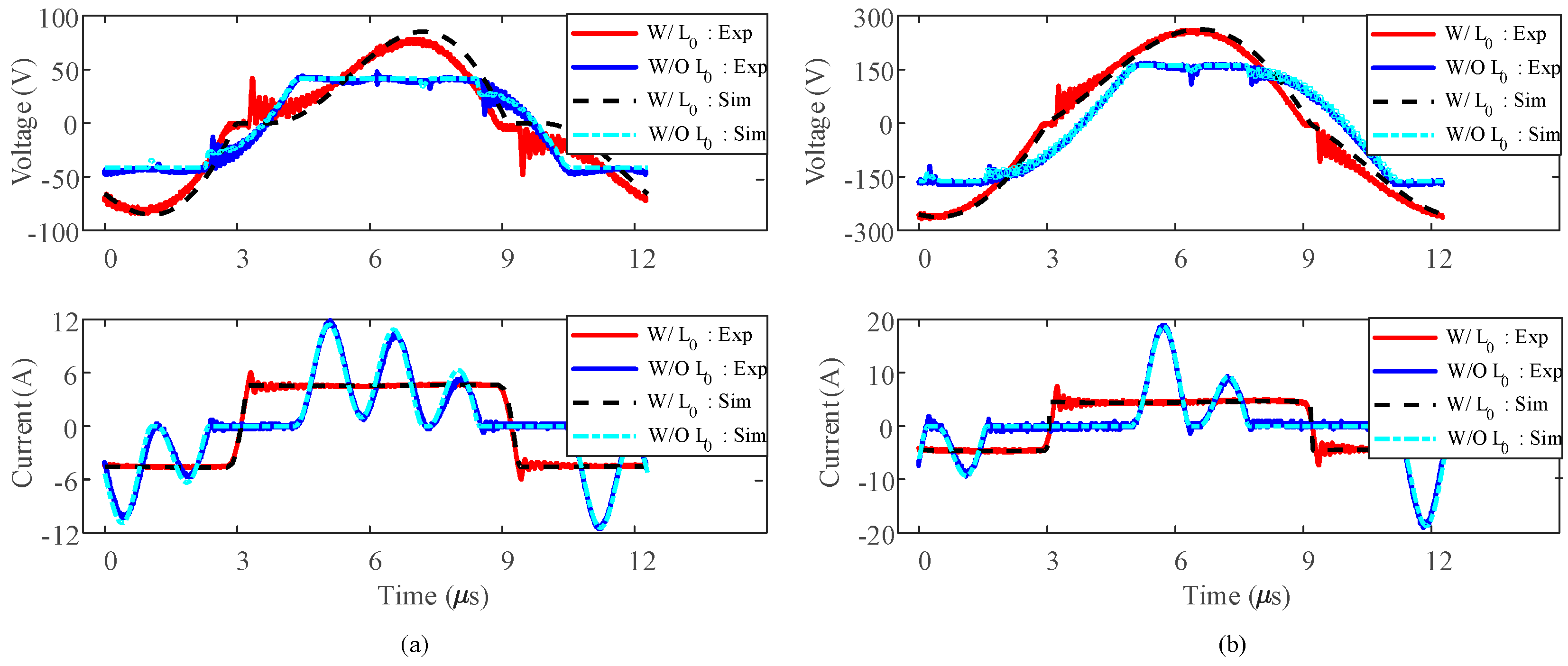
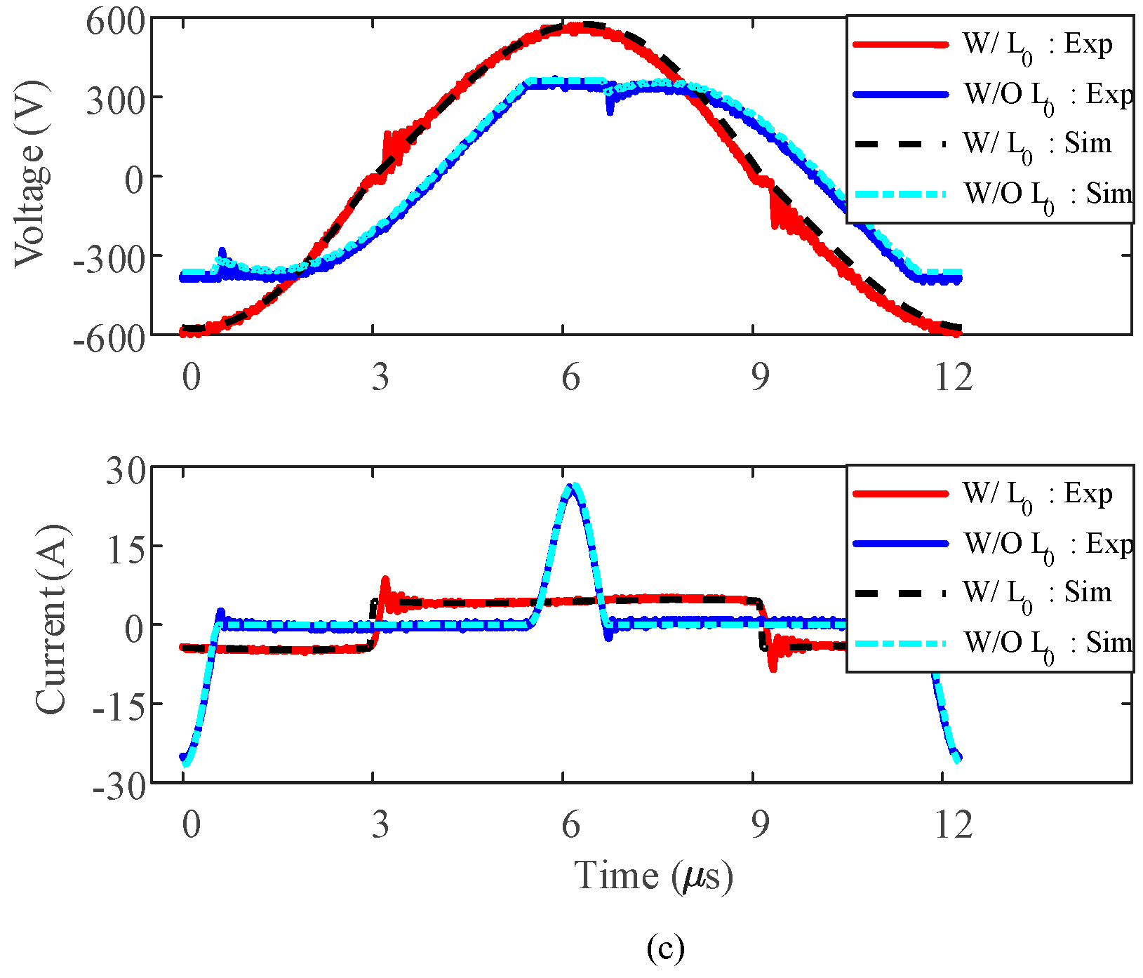
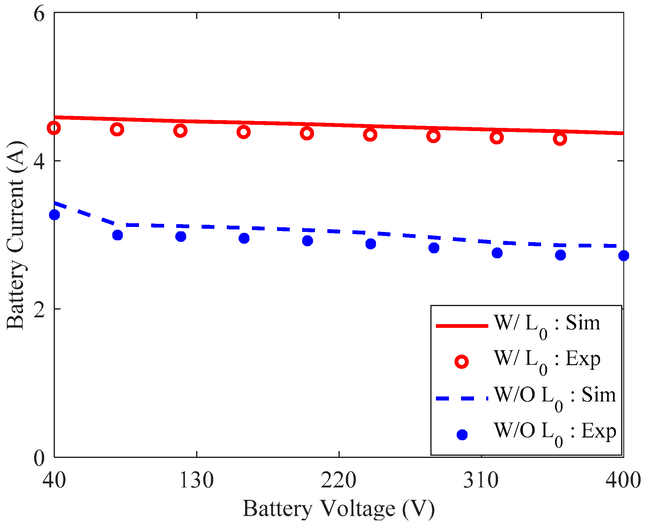
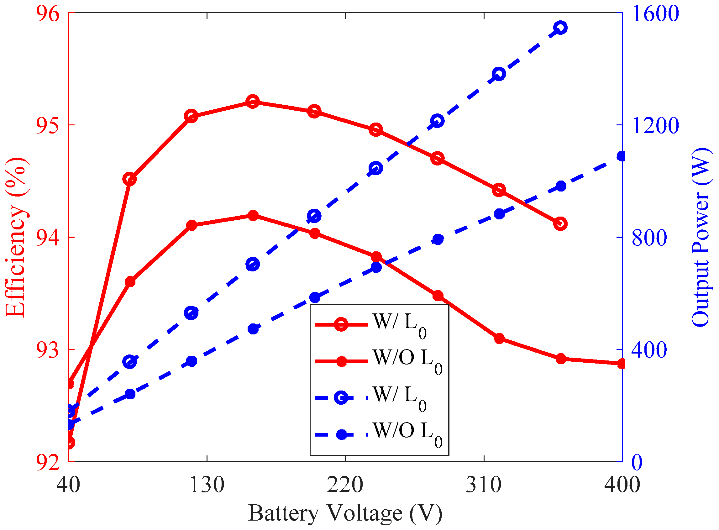
3.3. Eliminating L0
4. Conclusions
Author Contributions
Funding
Acknowledgments
Conflicts of Interest
References
- Li, S.Q.; Mi, C.C. Wireless Power Transfer for Electric Vehicle Applications. IEEE J. Emerg. Sel. Top. Power Electron. 2015, 3, 4–17. [Google Scholar]
- Zhang, Y.M.; Lu, T.; Zhao, Z.M.; He, F.B.; Chen, K.N.; Yuan, L.Q. Employing Load Coils for Multiple Loads of Resonant Wireless Power Transfer. IEEE Trans. Power Electron. 2015, 30, 6174–6181. [Google Scholar] [CrossRef]
- Liu, X.; Wang, T.F.; Yang, X.J.; Tang, H.J. Analysis of efficiency improvement in wireless power transfer system. IET Power Electron. 2018, 11, 302–309. [Google Scholar] [CrossRef]
- Momeneh, A.; Castilla, M.; Ghahderijani, M.M.; Miret, J.; de Vicuna, L.G. Analysis, design and implementation of a residential inductive contactless energy transfer system with multiple mobile clamps. IET Power Electron. 2017, 10, 875–883. [Google Scholar] [CrossRef]
- Buja, G.; Rim, C.T.; Mi, C.T.C. Dynamic Charging of Electric Vehicles by Wireless Power Transfer. IEEE Trans. Ind. Electron. 2016, 63, 6530–6532. [Google Scholar] [CrossRef]
- Kan, T.; Mai, R.; Mercier, P.P.; Mi, C. Design and Analysis of a Three-Phase Wireless Charging System for Lightweight Autonomous Underwater Vehicles. IEEE Trans. Power Electron. 2018, 33, 6622–6632. [Google Scholar] [CrossRef]
- Yan, Z.; Zhang, K.; Wen, H.; Song, B. Research on characteristics of contactless power transmission device for autonomous underwater vehicle. In Proceedings of the OCEANS 2016, Shanghai, China, 10–13 April 2016. [Google Scholar]
- Zhang, K.H.; Yan, L.B.; Yan, Z.C.; Wen, H.B.; Song, B.W. Modeling and analysis of eddy-current loss of underwater contact-less power transmission system based on magnetic coupled resonance. Acta Phys. Sin. 2016, 65, 048401-1. [Google Scholar]
- Kim, S.; Covic, G.A.; Boys, J.T. Comparison of Tripolar and Circular Pads for IPT Charging Systems. IEEE Trans. Power Electron. 2018, 33, 6093–6103. [Google Scholar] [CrossRef]
- Villa, J.L.; Sallan, J.; Osorio, J.F.S.; Llombart, A. High-Misalignment Tolerant Compensation Topology For ICPT Systems. IEEE Trans. Ind. Electron. 2012, 59, 945–951. [Google Scholar] [CrossRef]
- Zhang, W.; Mi, C.C. Compensation Topologies of High-Power Wireless Power Transfer Systems. IEEE Trans. Veh. Technol. 2016, 65, 4768–4778. [Google Scholar] [CrossRef]
- Zhang, Y. Key Technologies of Magnetically-Coupled Resonant Wireless Power Transfer; Springer: Singapore, 2017. [Google Scholar]
- Valtchev, S.; Borges, B.; Brandisky, K.; Klaassens, J.B. Resonant Contactless Energy Transfer With Improved Efficiency. IEEE Trans. Power Electron. 2009, 24, 685–699. [Google Scholar] [CrossRef]
- Wang, C.S.; Covic, G.A.; Stielau, O.H. Investigating an LCL load resonant inverter for inductive power transfer applications. IEEE Trans. Power Electron. 2004, 19, 995–1002. [Google Scholar] [CrossRef]
- Thrimawithana, D.J.; Madawala, U.K. A Generalized Steady-State Model for Bidirectional IPT Systems. IEEE Trans. Power Electron. 2013, 28, 4681–4689. [Google Scholar] [CrossRef]
- Hou, J.; Chen, Q.H.; Wong, S.C.; Tse, C.K.; Ruan, X.B. Analysis and Control of Series/Series-Parallel Compensated Resonant Converter for Contactless Power Transfer. IEEE J. Emerg. Sel. Top. Power Electron. 2015, 3, 124–136. [Google Scholar]
- Su, Y.; Tang, C.; Wu, S.; Sun, Y. Research of LCL resonant inverter in wireless power transfer system. In Proceedings of the International Conference on Power System Technology, PowerCon 2006, Chongqing, China, 22–26 October 2006. [Google Scholar]
- Li, S.Q.; Li, W.H.; Deng, J.J.; Nguyen, T.D.; Mi, C.C. A Double-Sided LCC Compensation Network and Its Tuning Method for Wireless Power Transfer. IEEE Trans. Veh. Technol. 2015, 64, 2261–2273. [Google Scholar] [CrossRef]
- Li, W.H.; Zhao, H.; Deng, J.J.; Li, S.Q.; Mi, C.C. Comparison Study on SS and Double-Sided LCC Compensation Topologies for EV/PHEV Wireless Chargers. IEEE Trans. Veh. Technol. 2016, 65, 4429–4439. [Google Scholar] [CrossRef]
- Wang, Y.J.; Yao, Y.S.; Liu, X.S.; Xu, D.G. S/CLC Compensation Topology Analysis and Circular Coil Design for Wireless Power Transfer. IEEE Trans. Transp. Electr. 2017, 3, 496–507. [Google Scholar] [CrossRef]
- Jeong, S.Y.; Kwak, H.G.; Jang, G.C.; Choi, S.Y.; Rim, C.T. Dual-purpose Non-overlapping Coil Sets as Metal Object and Vehicle Position Detections for Wireless Stationary EV Chargers. IEEE Trans. Power Electron. 2018, 33, 7387–7397. [Google Scholar] [CrossRef]
- Zhang, K.H.; Du, L.N.; Zhu, Z.B.; Song, B.W.; Xu, D.M. A Normalization Method of Delimiting the Electromagnetic Hazard Region of a Wireless Power Transfer System. IEEE Trans. Electromagn. C 2018, 60, 829–839. [Google Scholar] [CrossRef]
- Zhang, Y.; Zhao, Z.; Jiang, Y. Modeling and analysis of wireless power transfer system with constant-voltage source and constant-current load. In Proceedings of the 2017 IEEE Energy Conversion Congress and Exposition (ECCE), Cincinnati, OH, USA, 1–5 October 2017. [Google Scholar]


| Note | Symbol | Value |
|---|---|---|
| Transmitter inductance | L1 | 49.57 μH |
| Receiver inductance | L2 | 49.05 μH |
| Compensation inductance | Lf | 24.8 μH |
| Transmitter-side parallel compensation capacitance | Cf | 153.4 nF |
| Transmitter-side series compensation capacitance | C1 | 153.4 nF |
| Transmitter-side series compensation capacitance | C2 | 77.6 nF |
| Filter inductance | L0 | 713 μH |
| Coupling coefficient | k | 0.36 |
| Number of turns | N1, N2 | 12 |
| Gap | d | 60 mm |
| Coil dimension | 200 mm × 200 mm | |
| Resonant frequency | f0 | 81.6 kHz |
© 2019 by the authors. Licensee MDPI, Basel, Switzerland. This article is an open access article distributed under the terms and conditions of the Creative Commons Attribution (CC BY) license (http://creativecommons.org/licenses/by/4.0/).
Share and Cite
Yan, Z.; Zhang, Y.; Song, B.; Zhang, K.; Kan, T.; Mi, C. An LCC-P Compensated Wireless Power Transfer System with a Constant Current Output and Reduced Receiver Size. Energies 2019, 12, 172. https://doi.org/10.3390/en12010172
Yan Z, Zhang Y, Song B, Zhang K, Kan T, Mi C. An LCC-P Compensated Wireless Power Transfer System with a Constant Current Output and Reduced Receiver Size. Energies. 2019; 12(1):172. https://doi.org/10.3390/en12010172
Chicago/Turabian StyleYan, Zhengchao, Yiming Zhang, Baowei Song, Kehan Zhang, Tianze Kan, and Chris Mi. 2019. "An LCC-P Compensated Wireless Power Transfer System with a Constant Current Output and Reduced Receiver Size" Energies 12, no. 1: 172. https://doi.org/10.3390/en12010172
APA StyleYan, Z., Zhang, Y., Song, B., Zhang, K., Kan, T., & Mi, C. (2019). An LCC-P Compensated Wireless Power Transfer System with a Constant Current Output and Reduced Receiver Size. Energies, 12(1), 172. https://doi.org/10.3390/en12010172