Bidirectional DC Converter with Frequency Control: Analysis and Implementation


Abstract
1. Introduction
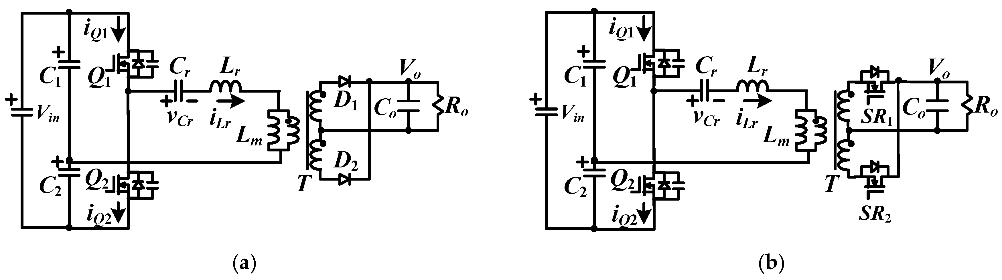
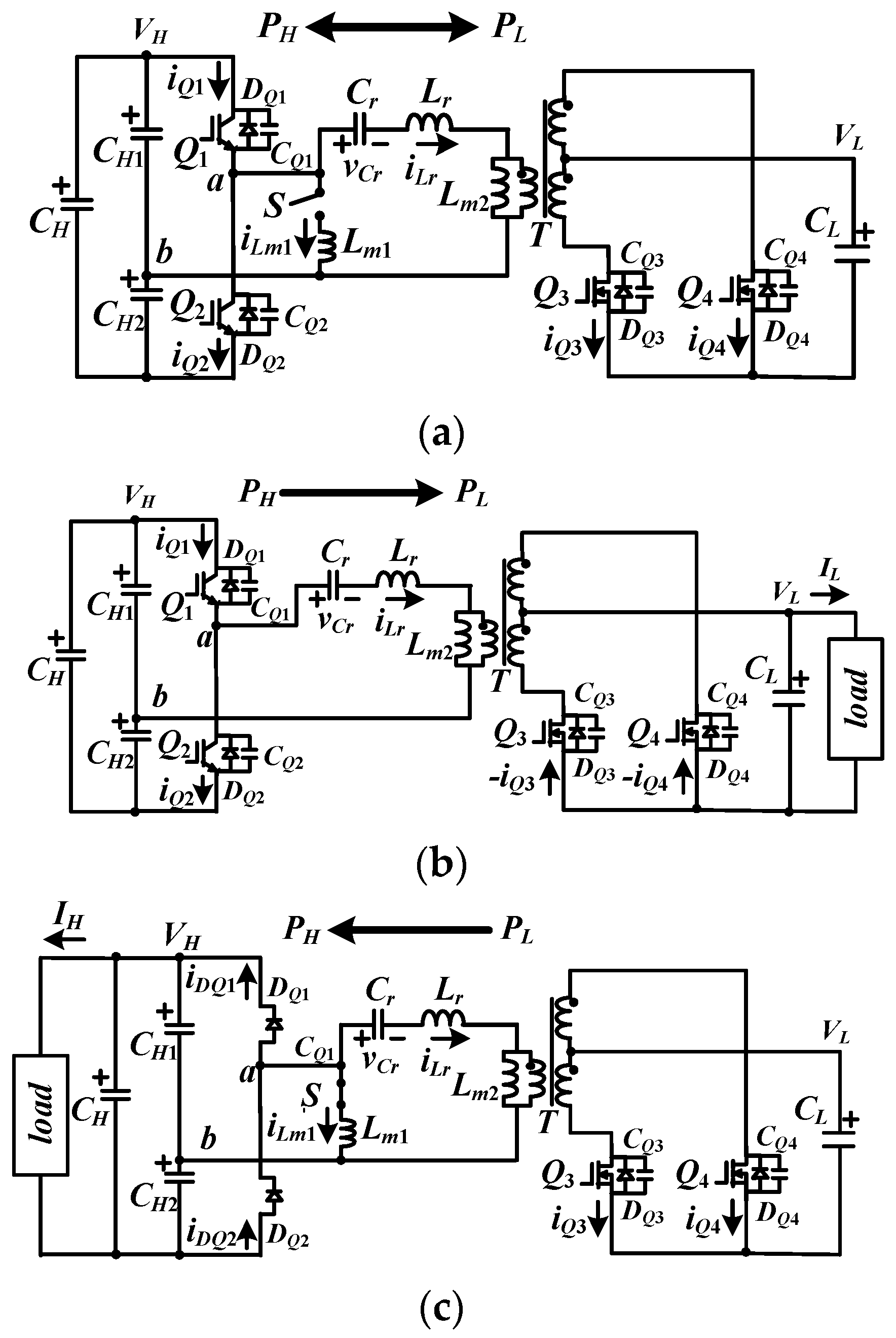
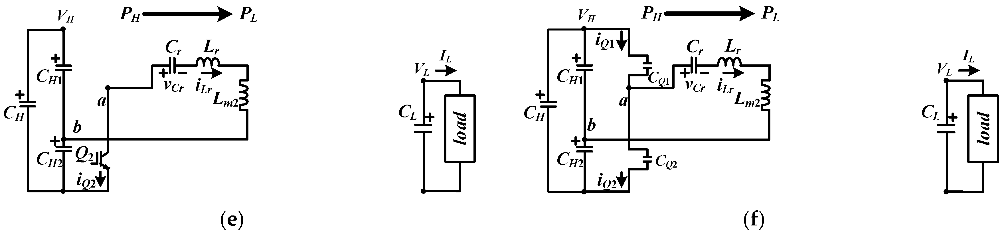
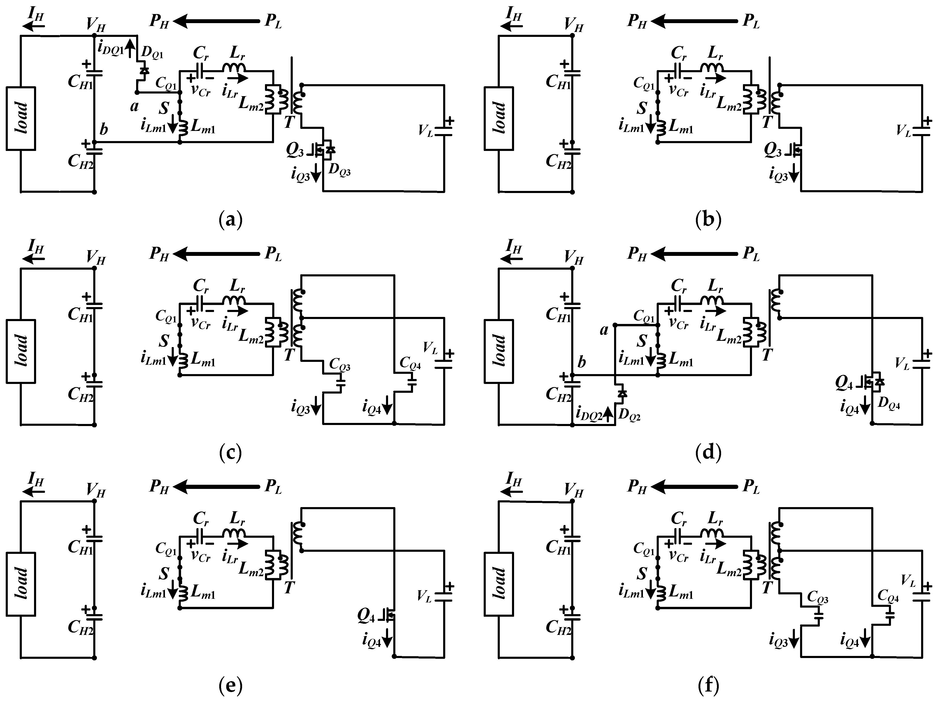
2. Circuit Diagram
3. Principles of Operation
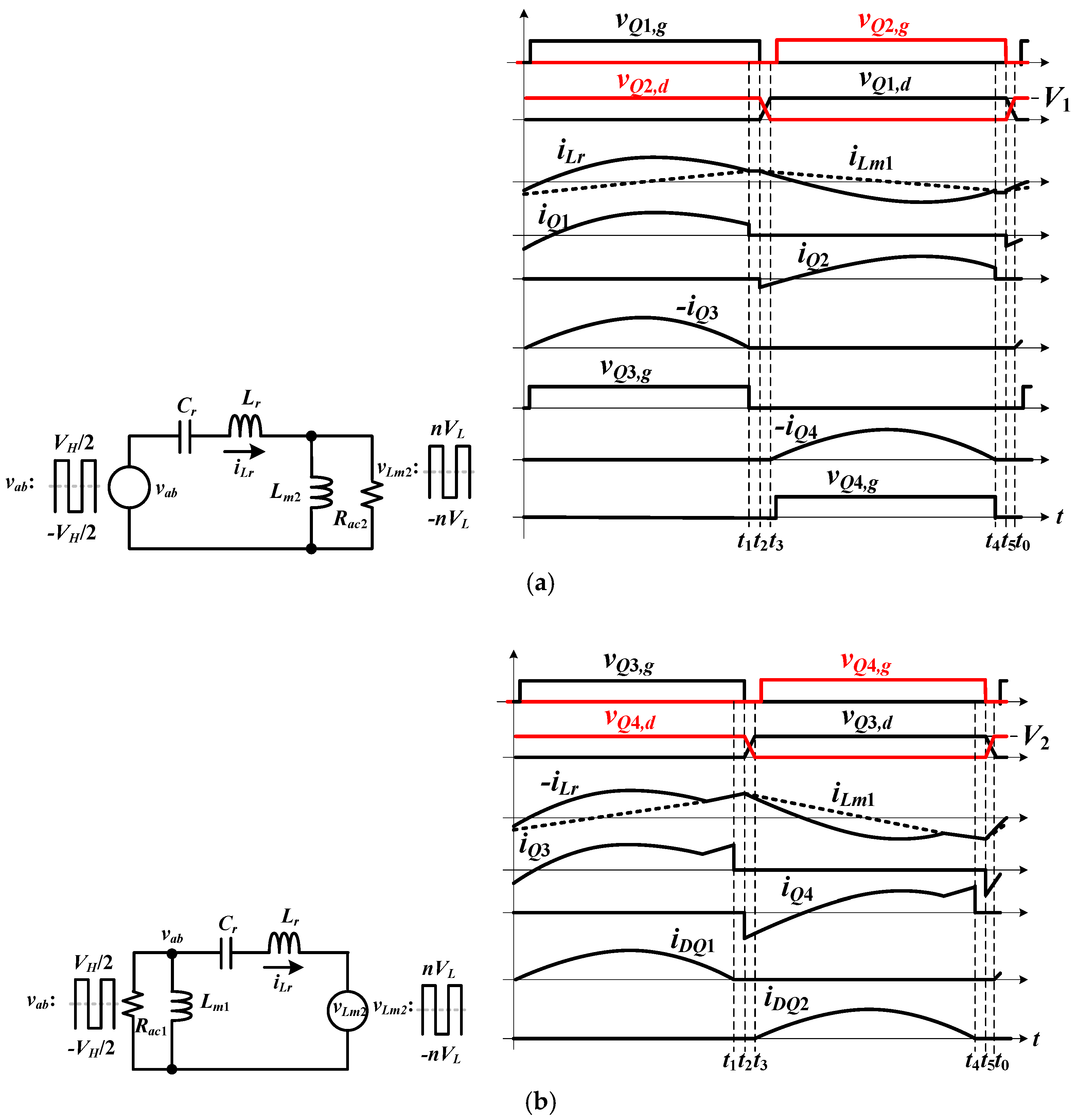
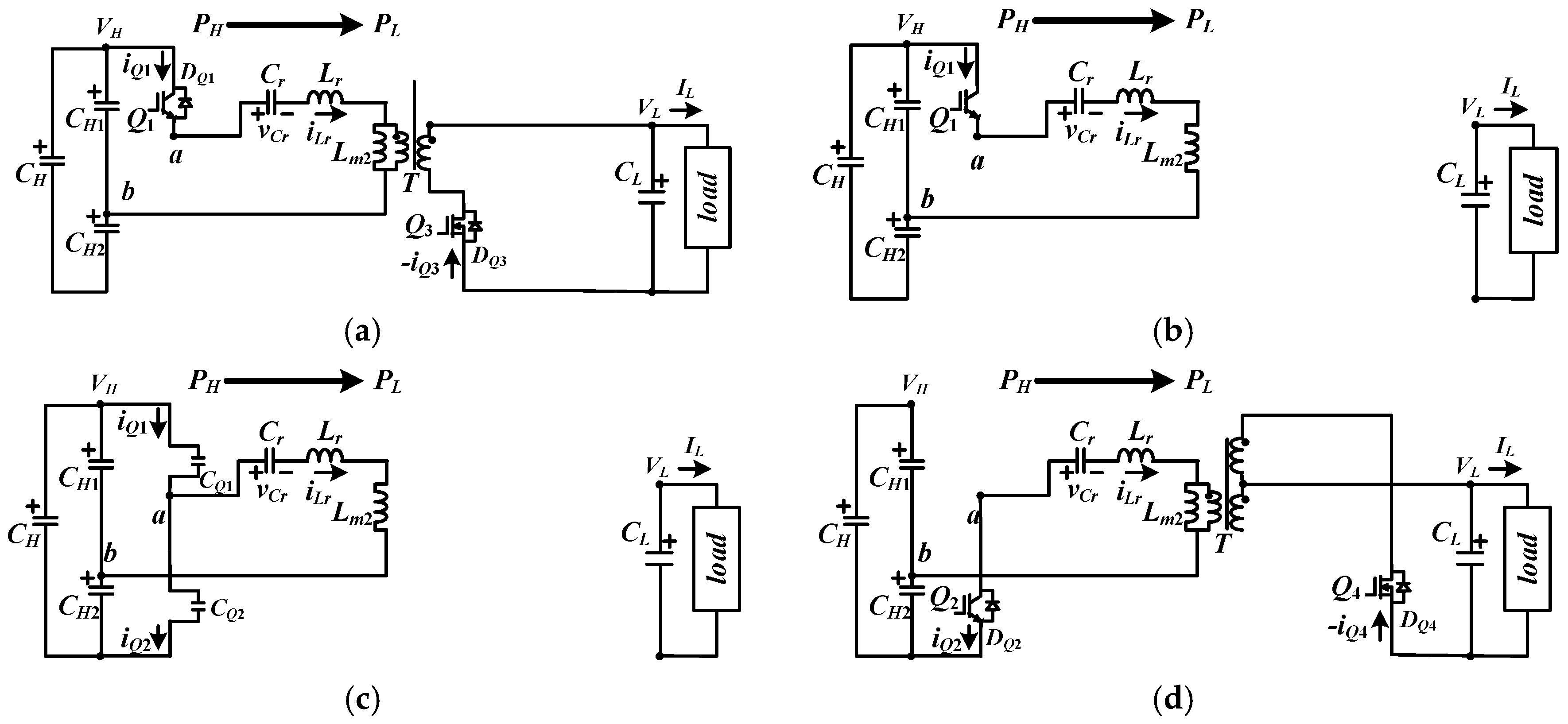
3.1. Forward Power Flow
3.2. Reverse Power Flow
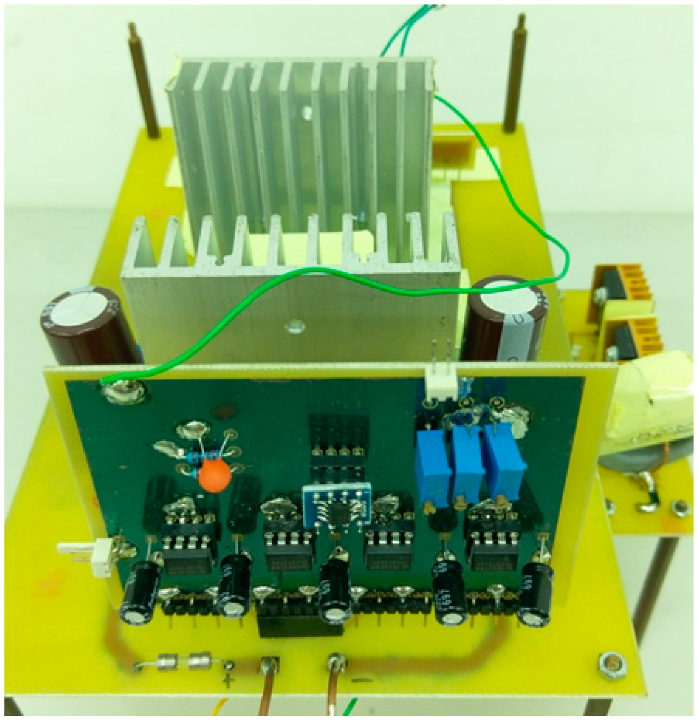
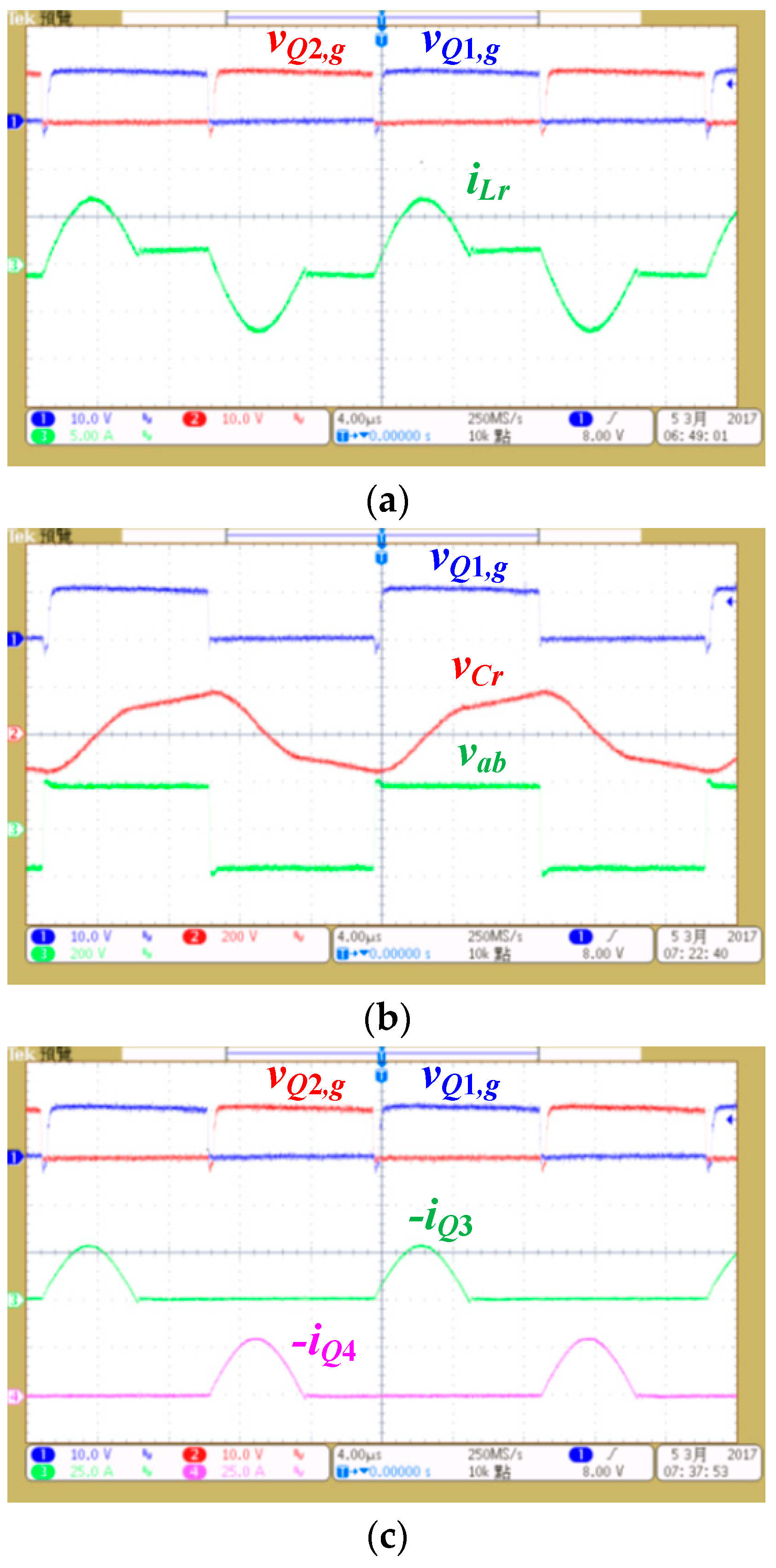
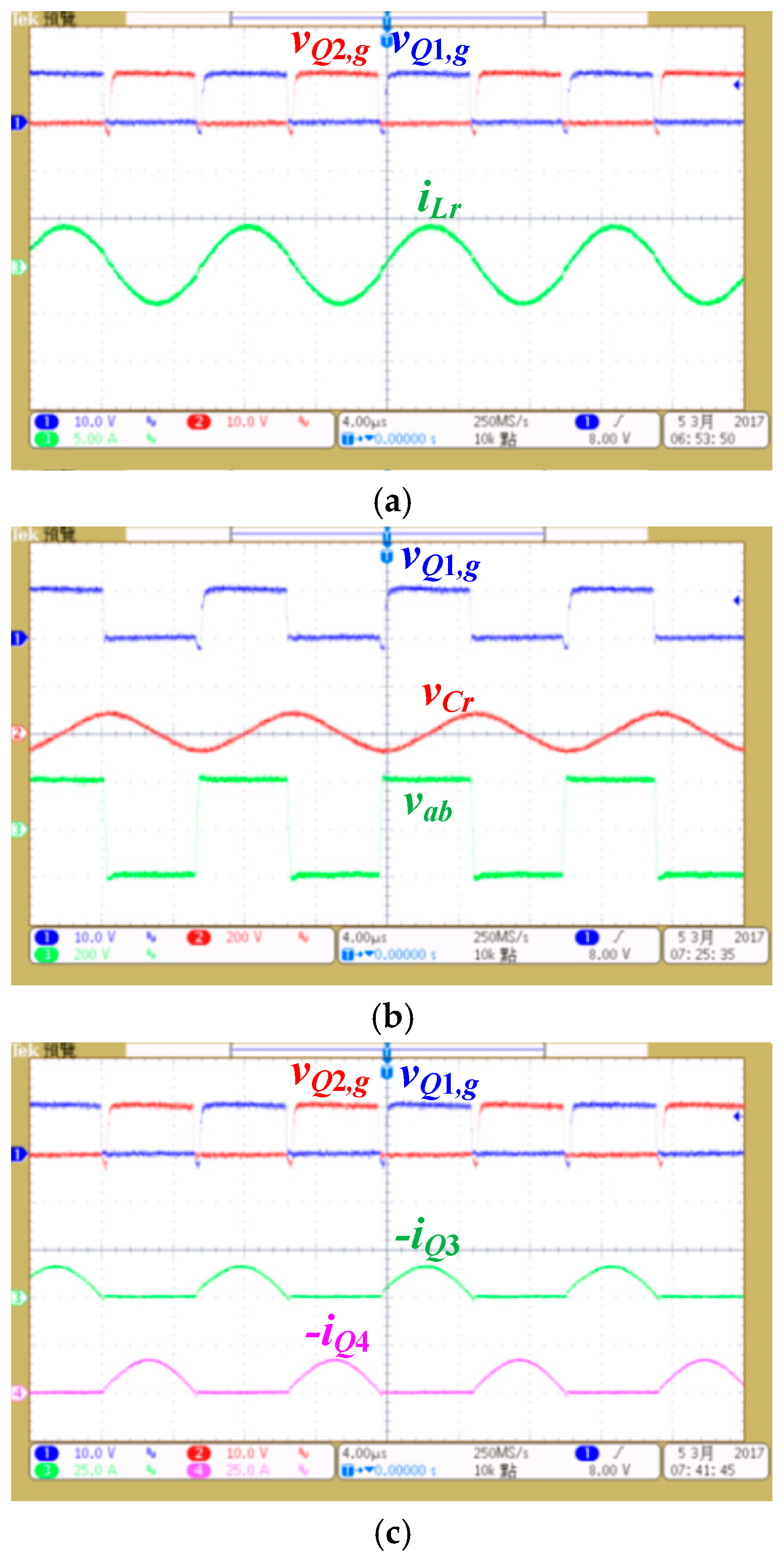
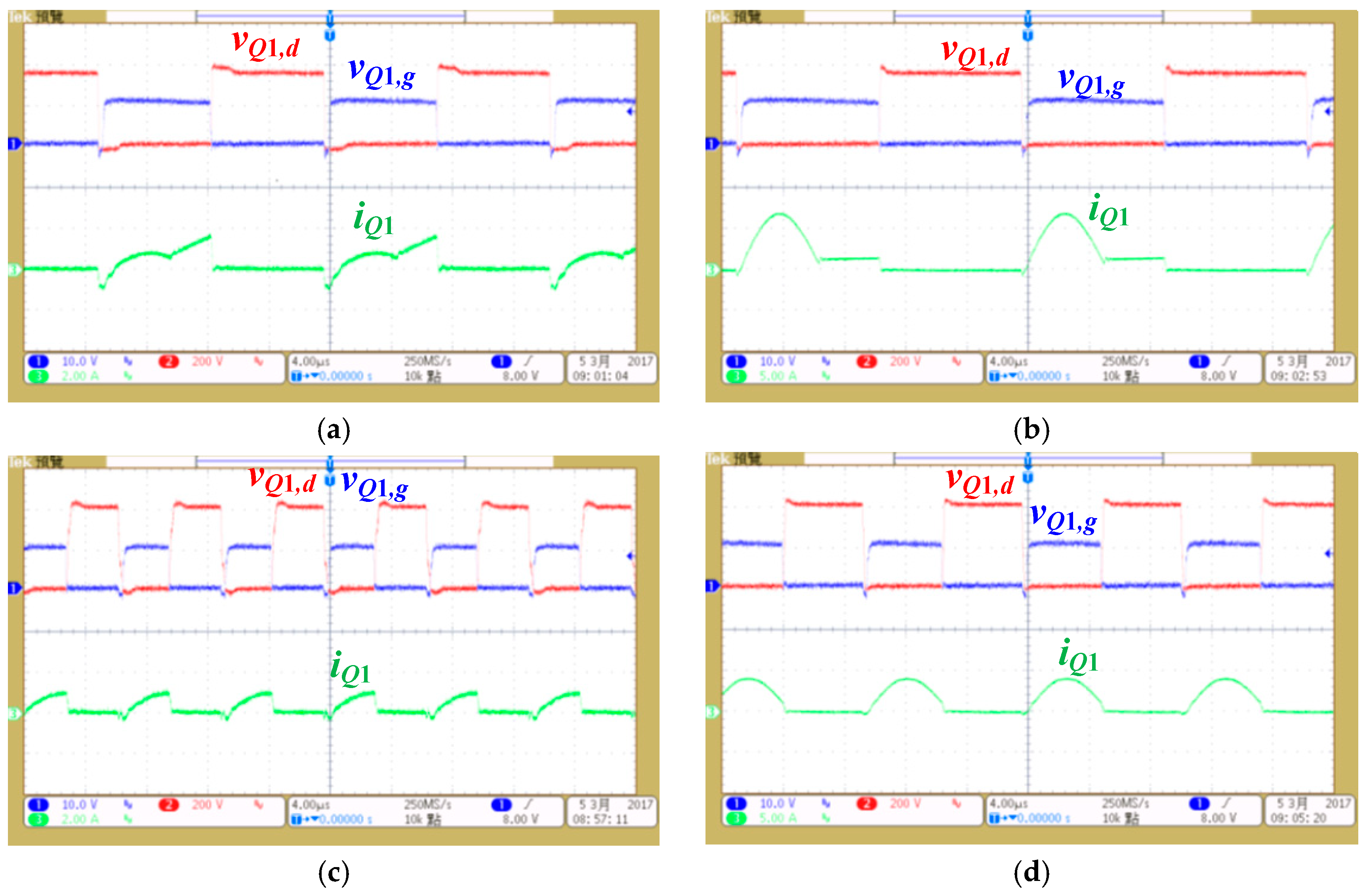
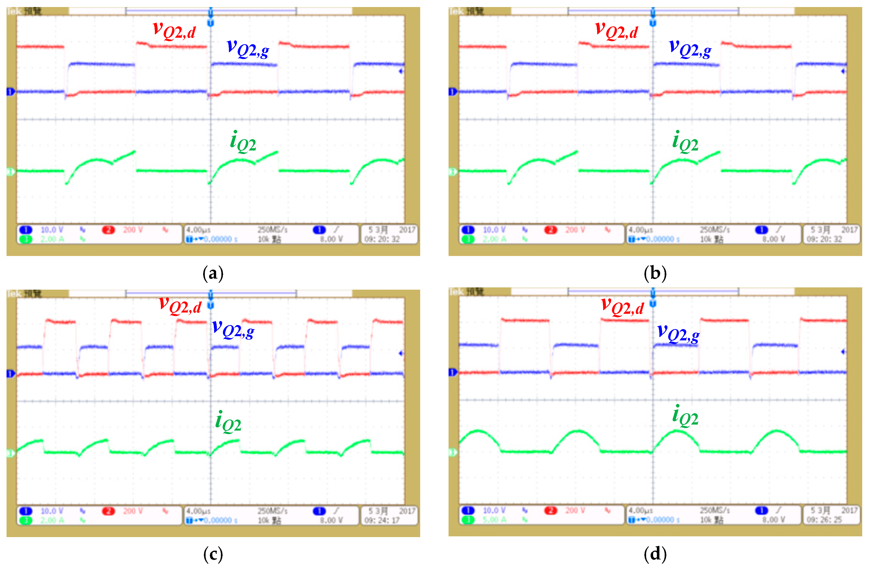
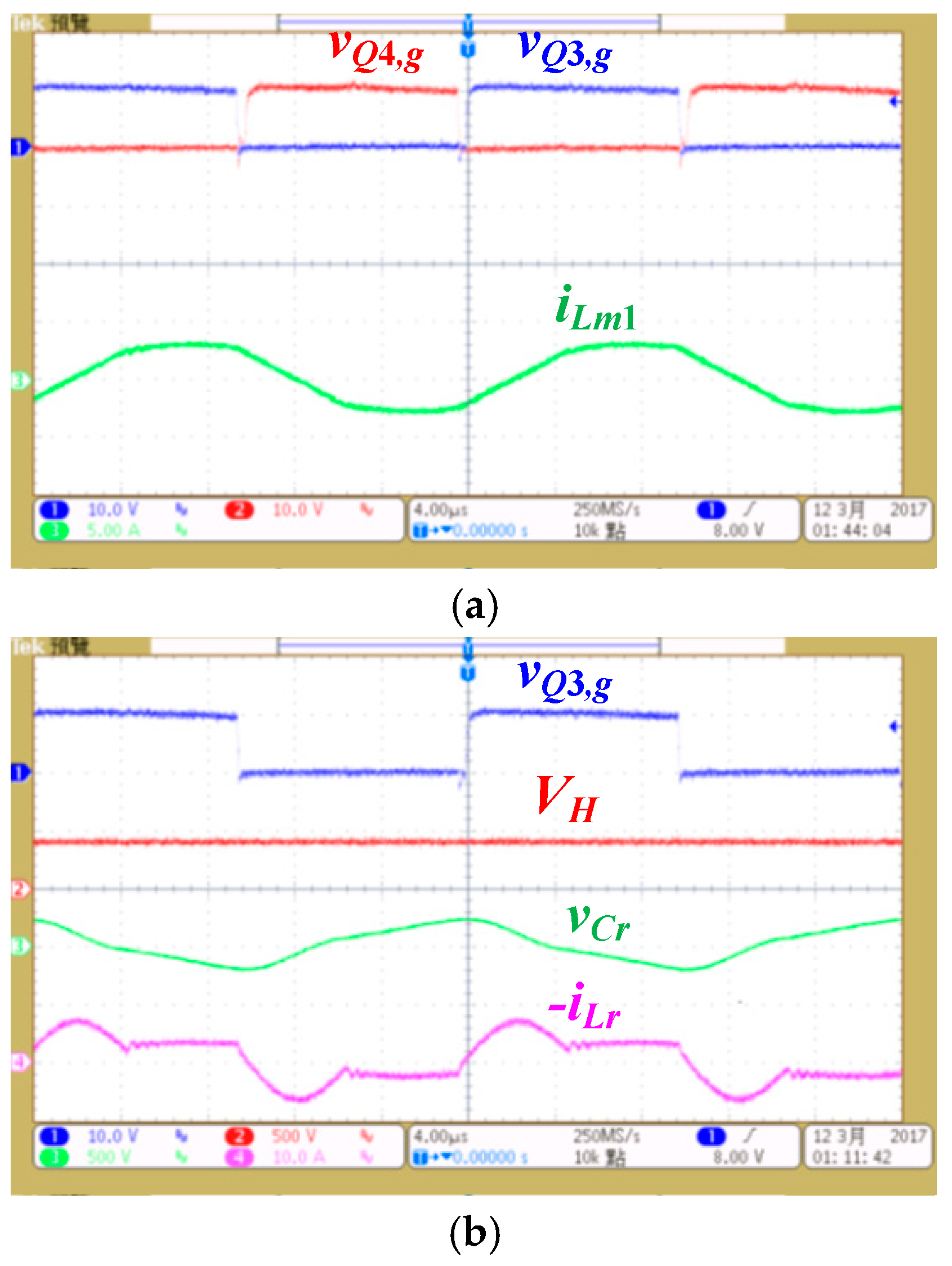
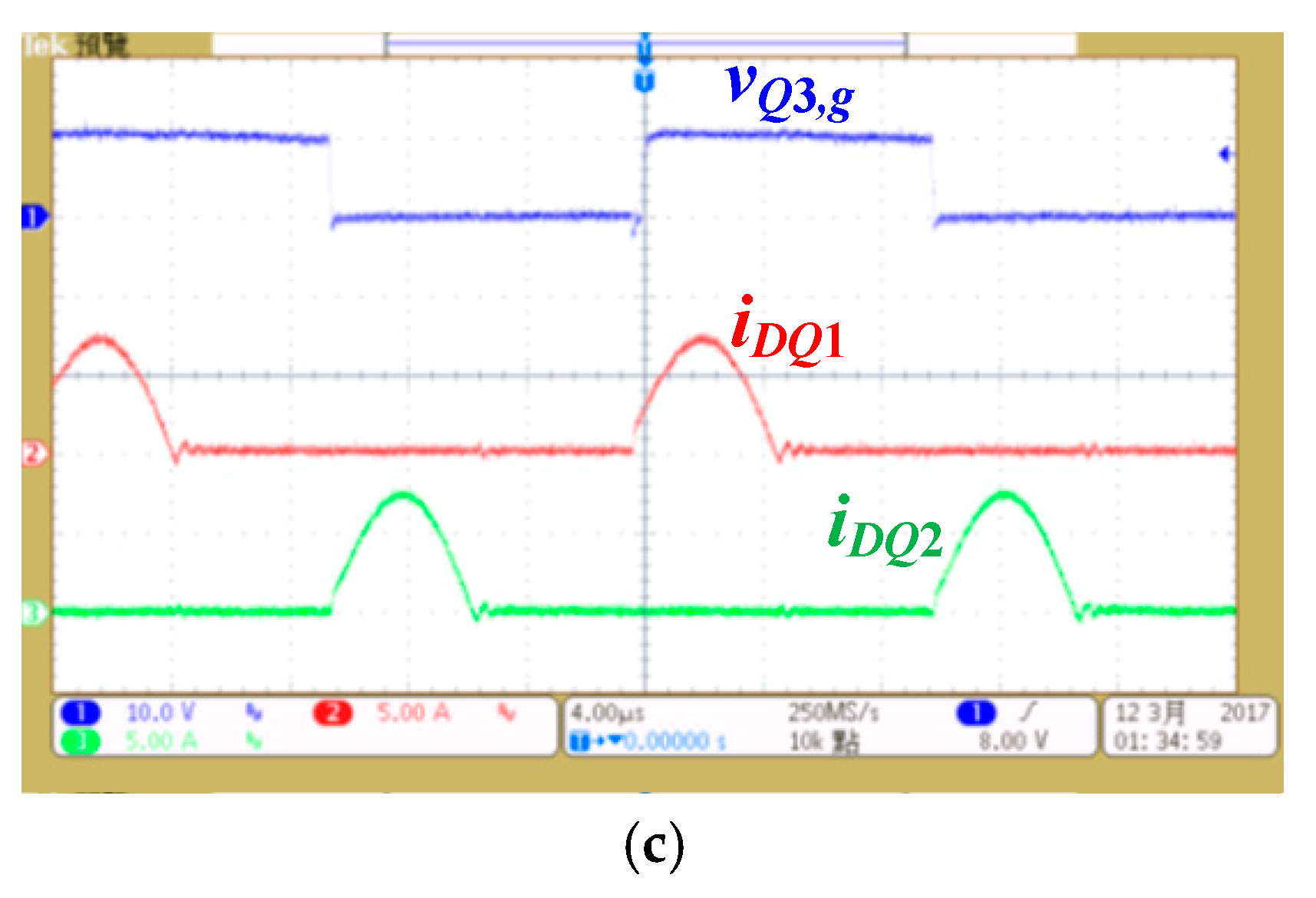
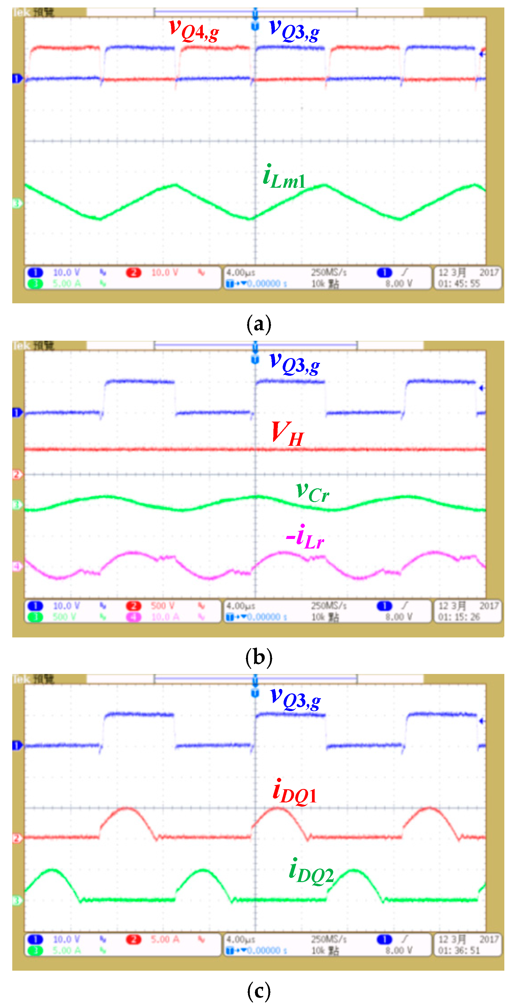
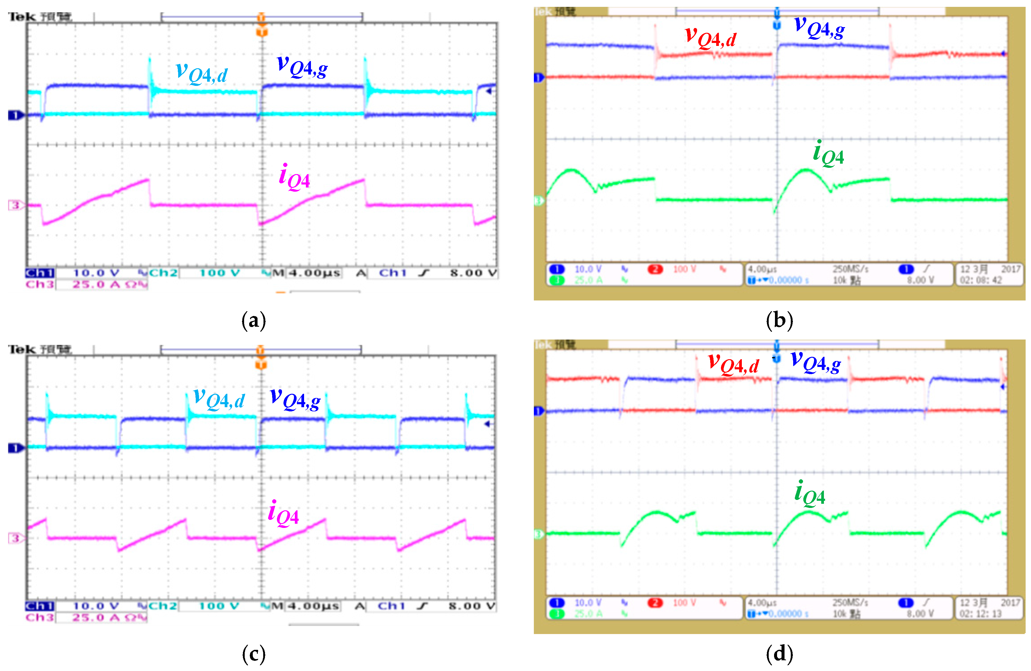
4. Experimental Waveforms
5. Conclusions
Author Contributions
Acknowledgments
Conflicts of Interest
References
- Zhao, J.F.; Jiang, J.G.; Yang, X.W. AC-DC-DC isolated converter with bidirectional power flow capability. IET Power Electron. 2010, 3, 472–479. [Google Scholar] [CrossRef]
- Singh, A.K.; Pathak, M.K. Single-phase bidirectional ac/dc converter for plug-in electric vehicles with reduced conduction losses. IET Power Electron. 2018, 11, 140–148. [Google Scholar] [CrossRef]
- Prasanna, U.R.; Singh, A.K.; Rajashekara, K. Novel bidirectional single-phase single-stage isolated ac-dc converter with PFC for charging of electric vehicles. IEEE Trans. Transport. Electrif. 2017, 3, 536–544. [Google Scholar] [CrossRef]
- Gu, L.; Jin, K. A three-phase bidirectional ac/dc converter with Y-Δ controlled transformers. IEEE Trans. Power Electron. 2016, 31, 8115–8125. [Google Scholar]
- Yilmaz, M.; Krein, P.T. Review of battery charger topologies, charging power levels, and infrastructure for plug-in electric and hybrid vehicles. IEEE Trans. Power Electron. 2013, 28, 2151–2169. [Google Scholar] [CrossRef]
- Emadi, A.; Lee, Y.J.; Rajashekara, K. Power electronics and motor drives in electric, hybrid electric, and plug-in hybrid electric vehicles. IEEE Trans. Ind. Electron. 2008, 55, 2237–2245. [Google Scholar] [CrossRef]
- Chan, C.C.; Chau, K.T. An overview of power electronics in electric vehicles. IEEE Trans. Ind. Electron. 1997, 44, 3–13. [Google Scholar] [CrossRef]
- Mishimay, T.; Hiraki, E.; Nakaoka, M. A High Frequency-Link Bidirectional DC-DC Converter for Super Capacitor-Based Automotive Auxiliary Electric Power Systems. J. Power Electron. 2010, 10, 27–33. [Google Scholar] [CrossRef]
- Krismer, F.; Biela, J.; Kolar, J.W. A Comparative Evaluation of Isolated Bi-directional DC/DC Converters with Wide Input and Output Voltage Range. In Proceedings of the Conference Record of the 2005 Industry Applications Conference, Hong Kong, China, 2–6 October 2005; pp. 599–606. [Google Scholar]
- Lee, J.Y.; Jeong, Y.S.; Han, B.M. A two-stage isolated/bidirectional DC/DC converter with current ripple reduction technique. IEEE Trans. Ind. Electron. 2012, 59, 644–646. [Google Scholar] [CrossRef]
- Zhang, Y.; Gao, Y.; Li, J.; Sumner, M. Interleaved switched-capacitor bidirectional dc-dc converter with wide voltage-gain range for energy storage systems. IEEE Trans. Power Electron. 2018, 33, 3852–3869. [Google Scholar] [CrossRef]
- Mangu, B.; Akshatha, S.; Suryanarayana, D.; Fernandes, B.G. Grid-connected PV-wind-battery-based multi-input transformer-couple bidirectional dc-dc converter for household applications. IEEE J. Emerg. Sel. Top. Power Electron. 2016, 4, 1086–1095. [Google Scholar] [CrossRef]
- Shen, C.L.; Shen, Y.S.; Chiu, P.C.; Liang, T.C. Isolated bidirectional converter with minimum active switches for high-voltage ratio achievement and micro-grid applications. IET Proc. Power Electron. 2017, 10, 2208–2216. [Google Scholar] [CrossRef]
- Pledl, G.; Tauer, M.; Buecherl, D. Theory of operation, design procedure and simulation of a bidirectional LLC resonant converter for vehicular applications. In Proceedings of the 2010 IEEE Vehicle Power and Propulsion Conference, Lille, France, 1–3 September 2010; pp. 1–5. [Google Scholar]
- Tan, K.; Yu, R.; Guo, S.; Huang, A.Q. Optimal design methodology of bidirectional LLC resonant DC/DC converter for solid state transformer application. In Proceedings of the IECON 2014—40th Annual Conference of the IEEE Industrial Electronics Society, Dallas, TX, USA, 29 October–1 November 2014; pp. 1657–1664. [Google Scholar]
- Kim, E.S.; Park, J.H.; Jeon, Y.S.; Kong, Y.S.; Lee, S.M.; Kim, K. Bidirectional secondary LLC resonant converter using auxiliary switches and inductor. In Proceedings of the 2014 IEEE Applied Power Electronics Conference and Exposition (APEC 2014), Fort Worth, TX, USA, 16–20 March 2014; pp. 1941–1947. [Google Scholar]
- Jiang, T.; Zhang, J.; Wu, X.; Sheng, K.; Wang, Y. A bidirectional LLC resonant Converter with automatic forward and backward mode transition. IEEE Trans. Power Electron. 2015, 30, 757–770. [Google Scholar] [CrossRef]
- Lin, B.R.; Chu, C.W. DC/DC converter with parallel input and parallel output with shared power switches and rectifier diodes. IET Proc. Power Electron. 2015, 8, 814–821. [Google Scholar] [CrossRef]
- Matko, V.; Milanović, M. Temperature-compensated capacitance-frequency converter with high resolution. Sens. Actuators A Phys. 2014, 220, 262–269. [Google Scholar] [CrossRef]
- Azevedo, R.G.; Huang, W.; O’Reilly, O.M.; Pisano, A.P. Dual-mode temperature compensation for a comb-driven MEMS resonant strain gauge. Sens. Actuators A Phys. 2008, 144, 374–380. [Google Scholar] [CrossRef]
- Matko, V. Next generation AT-cut quartz crystal sensing devices. Sensors 2011, 11, 4474–4482. [Google Scholar] [CrossRef] [PubMed]
- Steigerwald, R. A comparison of half bridge resonant converter topologies. IEEE Trans. Power Electron. 1988, 3, 135–144. [Google Scholar] [CrossRef]


| Primary-Side | Secondary-Side | Component Counts | Control Scheme | |
|---|---|---|---|---|
| Proposed converter | Half-bridge circuit | Center-tapped circuit | 5 switches, 3 magnetic components, 1 resonant capacitor | Frequency control |
| Circuit topology in Reference [8] | Full-bridge circuit | Center-tapped circuit | 6 switches, 2 magnetic components | Duty cycle control |
| Circuit topology in Reference [9] | Full-bridge circuit | Full-bridge circuit | 8 switches, 2 magnetic components | Duty cycle control |
| Circuit topology in Reference [10] | Half-bridge circuit | Half-bridge circuit | 6 switches, 3 magnetic components, 1 resonant capacitor | Frequency control |
| Circuit topology in Reference [14] | Full-bridge circuit | Full-bridge circuit | 8 switches, 2 magnetic components, 1 resonant capacitor | Frequency control |
| Circuit topology in Reference [16] | Full-bridge circuit | Full-bridge circuit | 8 switches, 3 magnetic components, 2 resonant capacitors | Frequency control |
© 2018 by the authors. Licensee MDPI, Basel, Switzerland. This article is an open access article distributed under the terms and conditions of the Creative Commons Attribution (CC BY) license (http://creativecommons.org/licenses/by/4.0/).
Share and Cite
Lin, B.-R.; Huang, Y.-C. Bidirectional DC Converter with Frequency Control: Analysis and Implementation. Energies 2018, 11, 2450. https://doi.org/10.3390/en11092450
Lin B-R, Huang Y-C. Bidirectional DC Converter with Frequency Control: Analysis and Implementation. Energies. 2018; 11(9):2450. https://doi.org/10.3390/en11092450
Chicago/Turabian StyleLin, Bor-Ren, and Yen-Chieh Huang. 2018. "Bidirectional DC Converter with Frequency Control: Analysis and Implementation" Energies 11, no. 9: 2450. https://doi.org/10.3390/en11092450
APA StyleLin, B.-R., & Huang, Y.-C. (2018). Bidirectional DC Converter with Frequency Control: Analysis and Implementation. Energies, 11(9), 2450. https://doi.org/10.3390/en11092450