1. Introduction
Recently, multilevel power inverters have been popularly employed in many electronic applications [
1,
2]. For example, solid-state transformers (SST) and dc distribution systems, which are high voltage (HV) or medium voltage (MV) applications, essentially require the use of multilevel topologies [
3,
4,
5,
6,
7]. In multilevel topologies, three-level neutral-point-clamped (NPC) inverters have been widely used in MV and HV applications. Compared to two-level inverters, three-level NPC inverters have some advantages, as follows. NPC inverters have more output voltage levels than two-level inverters. Therefore, the output voltages of an NPC inverter are more similar to sinusoidal waves than other topologies and NPC inverters have less of a harmonic component on output voltage. Additionally, in NPC inverters, the voltage rating of the switching device can be half of the one used in two-level inverters. In addition, NPC inverters generate relatively less leakage current flowing through the ground paths, so electromagnetic interference (EMI) induced problems are relatively lower than the two-level inverters.
However, the NPC inverter has a major drawback associated with the neutral-point voltage located between the upper and the lower dc-link capacitors. The voltage between the positive dc-link rail and the neutral-point should be identical to the voltage across the neutral-point and the negative dc-link rail. Unfortunately, there is a voltage imbalance between the upper and lower capacitors. This voltage imbalance harms the stability of the system, and limits the switching operation of the power stage [
8,
9,
10,
11]. In order to mitigate the voltage imbalance, many strategies that are based on additional hardware configurations or control algorithms have been proposed, and have been successfully adapted in some applications [
12,
13,
14,
15,
16,
17,
18,
19,
20,
21,
22,
23,
24,
25]. In [
12,
13], additional circuits for dc-link balancing were proposed. Although these methods achieved the dc-link voltage balancing successfully, the increase in the cost and the losses were major defects. To avoid these disadvantages, several modulation techniques for single-phase three-level NPC inverters have been presented in [
14,
15,
16,
17,
18,
19,
20,
21]. Among these modulation techniques, the carrier-based pulse width modulation (CB-PWM) approaches have been extensively preferred due to their simplicity of implementation. In [
14], the offset voltage injection with the zero-sequence component in the reference voltage was presented. The zero-sequence component is calculated at every switching period based on the dc-link link voltage and the grid current. Another type of offset voltage injection method was discussed in [
15]. In this paper, the offset voltage with a distribution factor was added into the modulation signal. However, these strategies face difficulties in being implemented because they are a burden on the prediction of the line current and the avoidance of nonlinearity in the injection signal. Additionally, the exact parameter information is essential to implement these methods as the algorithms are highly dependent on the system parameters. In [
16], a simple signal injection method was proposed to balance out the dc-link capacitor voltages by utilizing the harmonic signal consisting of the dc-link voltage difference and the double frequency of the utility grid. The method can easily be implemented as well as reducing the harmonic distortion in the input current of the NPC inverter.
In this paper, the method proposed in [
16] was further extended and detailed. In the proposed method, an even harmonic signal was added to the reference signal, which is generated by the current controller. Compared to other harmonic injection methods, the proposed method showed less voltage distortion on the synthesized output voltage. Furthermore, fast voltage balancing performance was obtained with the proposed strategy. A 10-kW single-phase three-level NPC inverter was built and tested. Here, the input grid voltage was 943 V in root mean square (RMS) and the output dc-link voltage was 1.8 kV. To artificially create voltage imbalance conditions, an unbalanced load bank was attached to the individual capacitors in the dc-link. The proposed method was compared with the method suggested in [
14] through simulations. The experimental results are presented to validate the effectiveness of the proposed method. This paper is organized as follows. In
Section 2, the pole voltage of the NPC inverter is analyzed with the proposed offset voltage injection method. The theoretical analysis of control performance with the offset voltage is discussed in
Section 3. Simulations and experimental results with the proposed method are shown in
Section 4. Finally,
Section 5 concludes this paper.
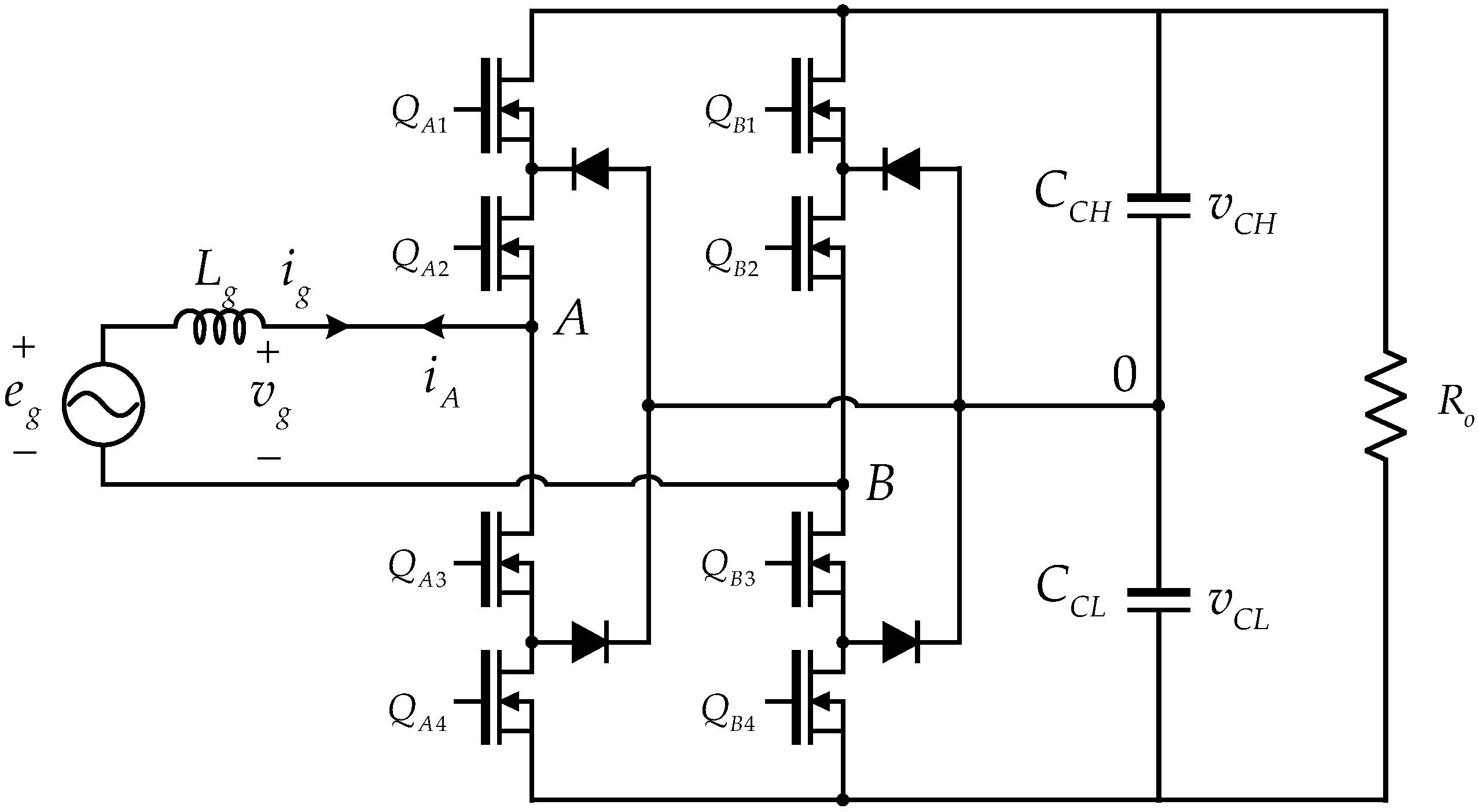
2. The Operation of the Single-Phase NPC Inverter and Its Neutral Current
Figure 1 illustrates a switching leg of the three-level NPC inverter and its conduction states. As shown in
Figure 1, the switching leg consists of four switching devices,
Qx1,
Qx2,
Qx3, and
Qx4, two clamping diodes,
D1 and
D2, and two dc-link capacitors,
CCH and
CCL. The pole voltage
vx0 has three different levels,
VCH, 0, and −
VCL according to the values of the switch function
Sx during the conduction periods, as shown in
Figure 1b–d. All parameters used in this paper are defined in
Table 1.
When
Sx = 1, the upper two devices,
Qx1 and
Qx2, are turned on. At this condition, shown in
Figure 1b, the output power is supplied by the upper dc-link capacitor
CCH, so that
vx0 becomes
VCH. If
Sx is 0, the middle switches,
Qx2 and
Qx3, conduct, and the output voltage is also clamped by the clamping diodes. Here, the amplitude of
vx0 is 0, and this state is illustrated in
Figure 1c. In
Figure 1d,
Sx is defined as −1, and the lower switching devices,
Qx3 and
Qx4, are closed. The output voltage is fed by the lower dc-link capacitor
CCL, and
vx0 becomes −
VCL.
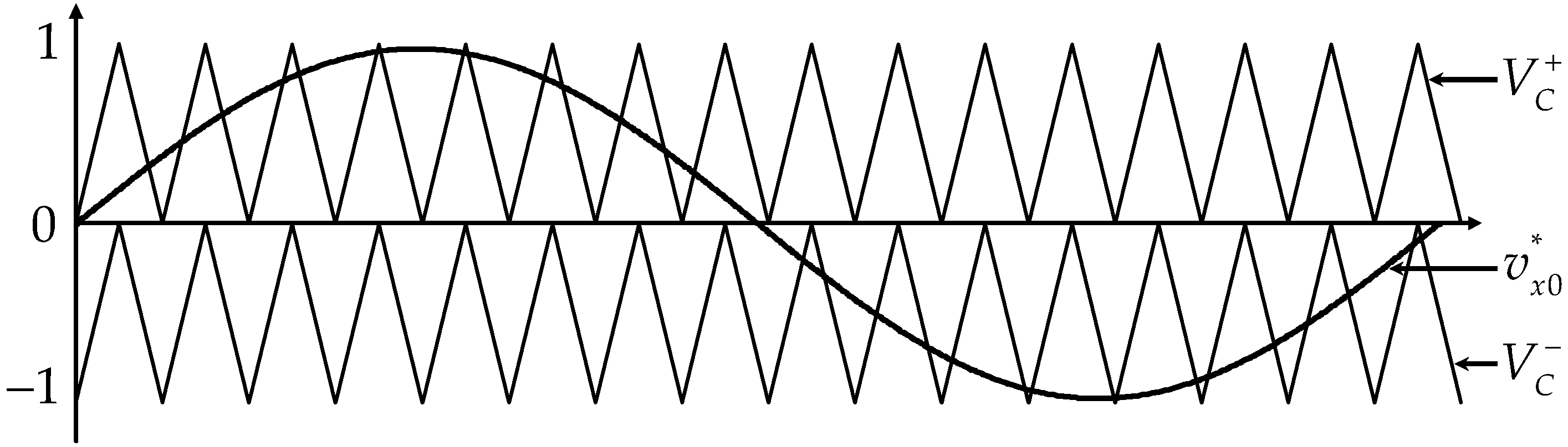
Figure 2 shows the normalized pole voltage reference
and two carrier signals
and
. Here,
is defined as Equation (1):
where
is the reference of the pole voltage. Equation (2) defines the relationships between the magnitudes of the carrier signals and the normalized pole voltage reference and the values of the switching function.
Let us consider that the switching frequency
fsw is much higher than the frequency of
. By doing so,
in the single switching period
Tc can be assumed as a constant value. Consequently, the on-time duration of the switch,
τx, is given as:
By using Equation (3), the average output pole voltage,
, over one switching period is simply written as follows:
If the upper and the lower capacitors have the same voltage,
VCH =
VCL = 0.5
VDC, the pole voltage shown in Equation (4) can be rewritten as:
In order to be placed in the linear modulation range, the following conditions should be satisfied.
Figure 3 represents the configuration of the single-phase three-level NPC inverter dealt with in this paper. Here, two three-level switching legs were employed. In each switching leg, the middle points of the clamping diodes were connected to the neutral point of the dc-link. By referring the notations in
Figure 3, the pole voltage references of the individual switching legs are written as follows:
where
and
are the line-to-line voltage reference and the virtual offset voltage between the switching pole
B and the neutral point of the dc-link, respectively. It should be noticed that both
and
should be operated in the linear modulation region. This means that they should satisfy the conditions expressed in Equation (6). In addition,
should be also placed in the linear modulation region, because
is identical to
. From this analysis, the following condition can be derived:
Equation (9) offers that various virtual offset voltages can be selected with various control purposes. The object of the approach taken in this paper was to balance the dc-link capacitor voltages. To do this, the second-order harmonic injection approach was proposed in this paper. Here,
is selected as Equation (10):
where
ω and
K are the fundamental electrical angular frequency of the grid voltage
eg and the injection gain of the second harmonic voltage, respectively. By substituting Equation (10) into Equations (7) and (8), the pole voltages are expressed as follows:
In
Figure 3, the voltage of the lower capacitor was adjusted by injecting the neutral current
idA and
idB, which are represented with the phase current from the switching pole
A to the grid
iA and the switching functions of each switching leg,
SA0 and
SB0, as follows.
The entire neutral current flowing into the neutral point is simply obtained as:
The average value of the neutral current over a single switching period is calculated as below:
where
is the average of
iA(
t) in the switching period. By applying the pole voltages, Equation (16) is rewritten as Equation (17).
By substituting Equations (11) and (12) into Equation (17),
is obtained, and is expressed in two ways according to the polarities of
and
. When the polarities of the pole voltage references are the same, the average neutral current is written as Equation (18).
If the polarities of
and
are different, Equation (19) is obtained.
By adjusting the pole voltage references, the average current expressed by Equations (18) or (19) is controlled to balance out the dc-link capacitors’ voltages.
3. Analysis of the Injected Offset Voltage
This section compares the proposed second-order harmonic injection method above-mentioned with the partially rectified wave injection method.
Figure 4 shows the pole voltage range which consisted of 0.5
VDC − max(
vg*,0) to −0.5
VDC − min(
vg*,0).
Figure 4a shows the pole voltage reference when there was no difference between upper and lower capacitor voltage in Equation (8). In this case, the pole voltage reference always satisfies the range of the pole voltage (Equation (9)).
Figure 4b shows the synthesized pole voltage reference where this method was proposed in [
15]. In this case, the offset voltage was composed of distribution factor
μ and the absolute value of the phase voltage reference. This method can cover the full range of dc-link capacitor voltage difference, but this offset signal injection method requires repetitive calculation since the absolute values are used in Equation (17).
Figure 4c shows the synthesized pole voltage where the offset voltage composed of the dc-link capacitor voltage difference and the fundamental component was injected instead of the second-order harmonic component in the pole voltage reference (Equation (9)). In this case, the maximum value of the pole voltage reference was 0.5 m
VDC + K at π/2, and the minimum value of the pole voltage reference was −0.5 m
VDC −
K at 3π/2. Therefore, the voltage difference that can be injected for the dc-link capacitor voltage balance is restricted by modulation index m.
Figure 4d shows the pole voltage where the offset voltage is composed of the dc-link capacitor voltage difference and the second-order harmonic component. In this case, the maximum value can be found by calculating the divergence of the pole voltage
vA0*. Solving Equation (20) equal to zero, the roots are as follows:
Among these roots, the maximum value and the minimum value exist at:
The other roots are imaginary roots when the value of K is below the specific value determined by the modulation index m. In addition, the offset voltage vz* can be considered, which is composed with the voltage difference K and the half-wave rectified by the second-order harmonic component. In this case, the maximum value of the pole voltage vA0* is the same as the condition that injected the second-order harmonic component, but the minimum value was the same as the condition where the dc-link voltage difference is zero. The reason each injection voltage was inserted in a subdivided way as follows: for the 0 to π/2 region, the voltage difference was reduced, but within the next π/2 to π region, the offset voltage signal made switching operations for each leg to diverge. In this region, the switching state of leg A was increased to a 0 state and the switching state of leg B was increased to a −1 state by a synthesized reference signal. Consequently, a new reference signal increase the voltage difference, which turned on more low-side switches than the high-side ones. Therefore, the injection voltage had to be inserted in a subdivided way.
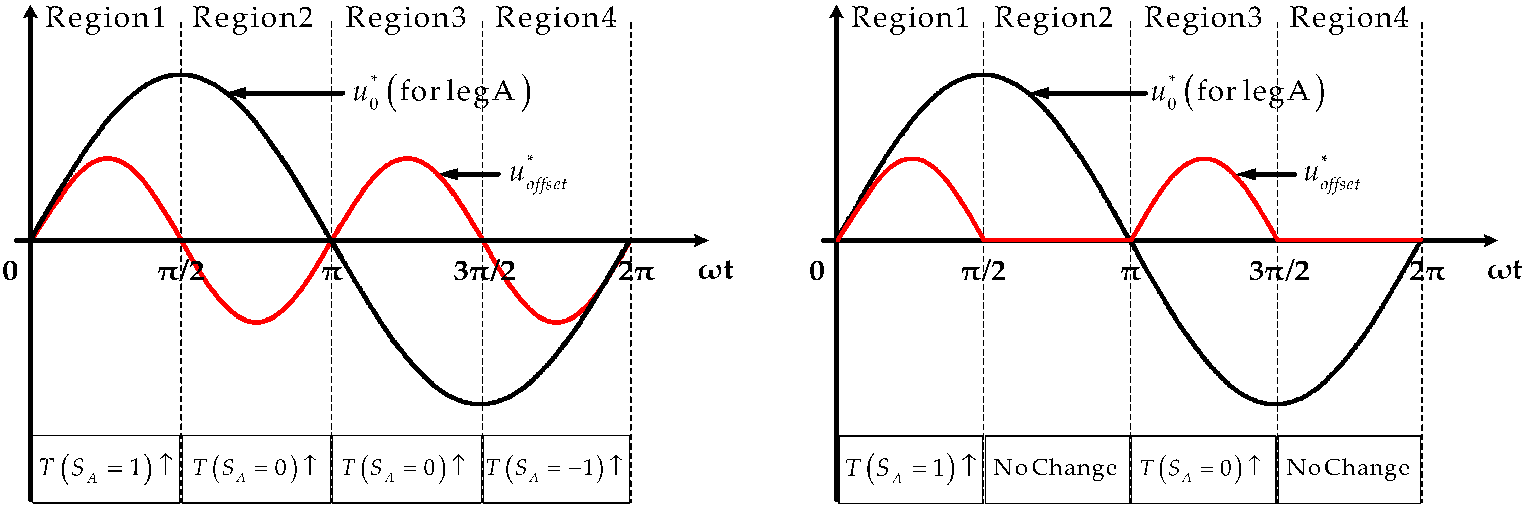
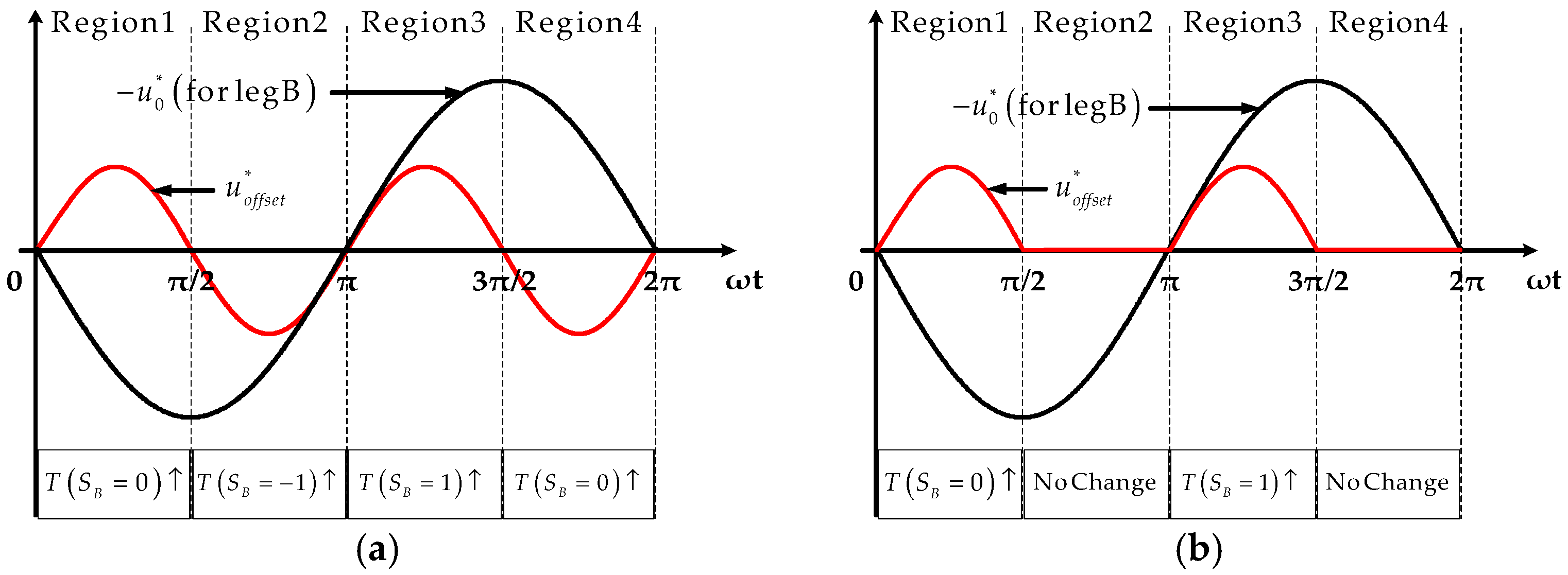
Figure 5 shows the waveforms which are reference signal for legs A, B, and the offset signal that has double the frequency of the reference signal. In addition, it also shows that the switching operation changed every π/2 cycle, when the reference signal and offset signal were synthesized. In
Figure 5a, Region 1, the switching operation for leg A was increased to a 1 state by the synthesized reference signal with the offset signal (
SA = 1). On the other hand, the switching operation for leg B was increased to the 0 state (
SB = 0). In Region 2, the offset signal had a negative value. Therefore, the switching operation for leg A was increased to the 0 state (
SA = 0). In the same manner, the switching operation for leg B was increased to the −1 state (
SB = −1). In Region 3, the reference signal had a negative value and the offset signal had a positive value. The switching operation for leg A was increased to the 0 state (
SA = 0), and for leg B it was increased to the 1 state (
SB = 1). In Region 4, the switching operation for leg A was increased to the −1 state (
SA = −1) and for leg B, it was increased to the 0 state (
SB = 0). In
Figure 5b, the switching operation states for leg A and leg B could be easily observed by comparing it with
Figure 5a. In Regions 1 and 3, the increased switching state for each leg, (
SA,
SB), were (1,0) and (0,1), respectively. In Regions 2 and 4, there was no offset signal, so the synthesized reference signals were the same as the reference signal.
The maximum and minimum values obtained from the previous equations were determined by the voltage difference
K and modulation index
m. With the same modulation index
m, the offset voltage injection method with distribution factor
μ could be adopted for the full range of capacitor voltage difference such as from 0 V to
VDC, but there were voltage oscillations on the dc-link voltage when the balancing control was adopted [
15]. In contrast, the offset voltage injection method with the second-order harmonic component or the half-wave rectified can be adopted for smooth control. Furthermore, the proposed method could easily configure the controller using Equations (11), (12), and (22), and the PWM modulator described in
Figure 6. However, the proposed method has limitations on the range of capacitor voltage difference given the effects of the voltage difference of the dc-link capacitor on the injection signal. This could be a larger reference signal than the previous reference signal for dc-link voltage control. In this case, an over-distorted reference signal could not control either the dc-link voltage control or dc-link capacitor voltage balancing control. The voltage range of the proposed method is up to the point where the remaining two roots other than the maximum and minimum are zero when the modulation index m is constant in Equation (21).
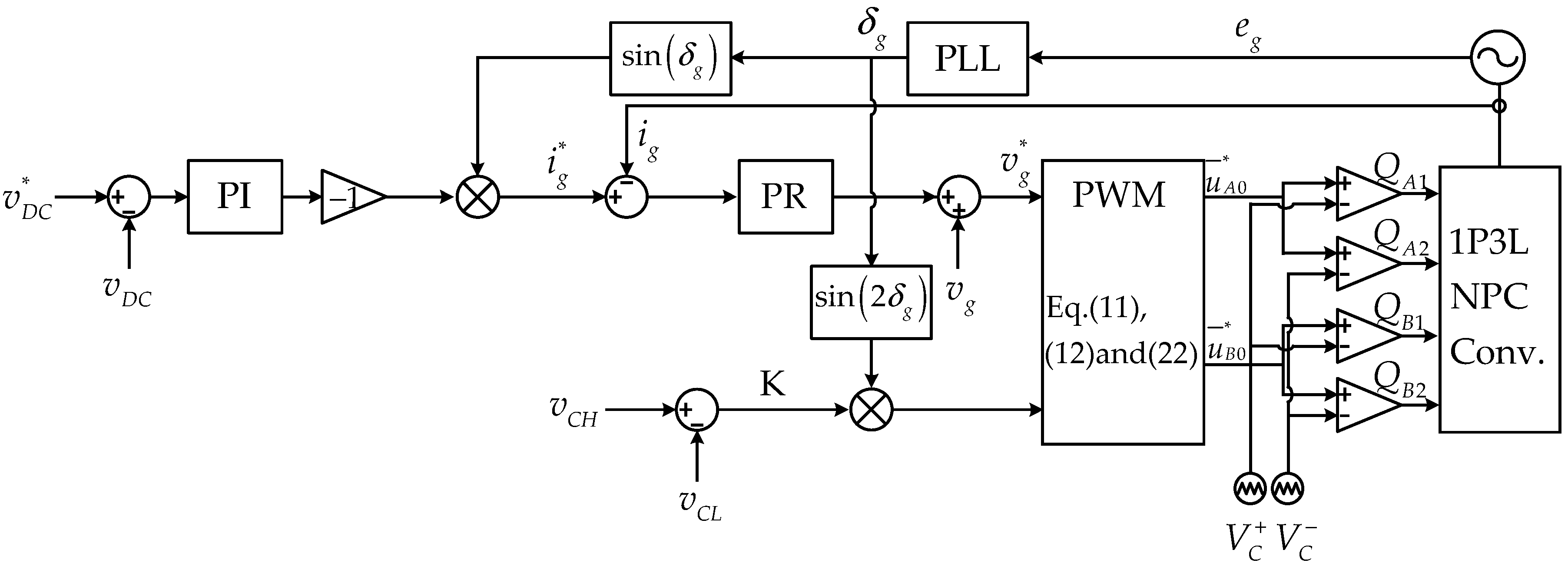
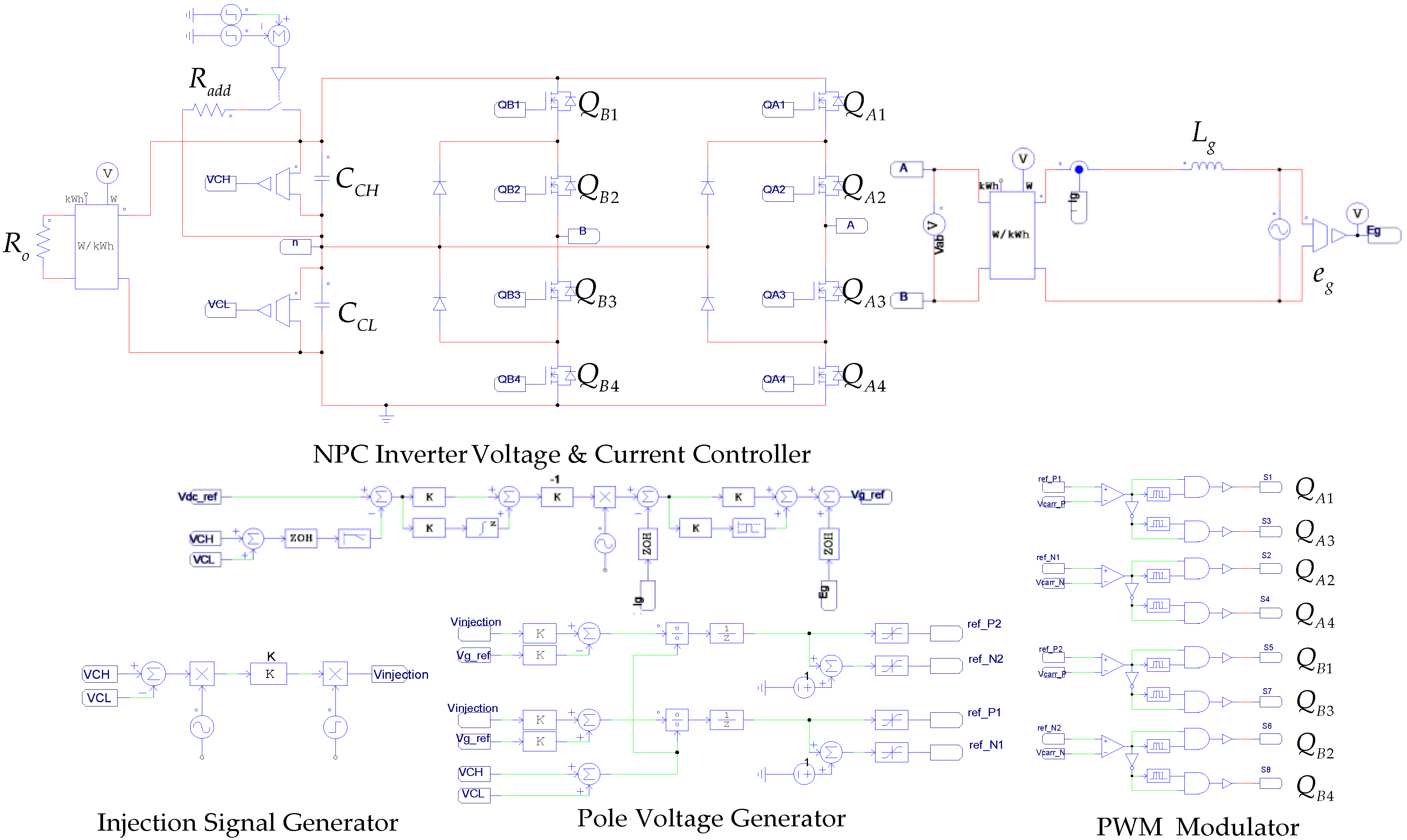
4. Simulation and Experimental Results
Simulations and experiments for the single-phase three-level NPC inverter were performed to verify the effectiveness of the proposed half-wave of the even-harmonics voltage injection method. In addition, these simulations and experiments were done in a single-phase NPC circuit structure with an additional resistive load circuit on top of the dc-link capacitor, as shown in
Figure 2. The proposed dc-link capacitor voltage balancing control and the conventional method were carried out in a PSIM simulation, and the simulation scheme is shown in
Figure 7. The controller contained three blocks to generate the modulation signal: the PI controller for dc-link capacitor voltage control, PR controller for input current control, and the proposed capacitor voltage balancing controller. The control sequence for the dc-link capacitor voltage balance is as follows. The NPC inverter operates as a general PWM rectifier that traces the dc-link capacitor voltage reference with the PI and PR controller before the capacitor voltage imbalance occurs. In this case, the offset signal
vz* in Equations (10) and (11) is zero because there is no voltage difference on the dc-link capacitor, so the coefficient of
vz*,
K, is zero. When a voltage difference occurs, the balancing control operates to reduce the voltage difference. The parameters for balancing control are obtained as follows: the capacitor voltage (
VCH,
VCL) and input current
ig are measured by the voltage and current sensor, respectively. The grid voltage phase angle,
δg, is calculated from the phased locked loop (PLL) scheme by measuring grid voltage
eg. At this point, the PWM modulator generates a new pole voltage reference by synthesizing the reference signal and offset signal.
In the simulation, the dc-link capacitor voltage difference between the upper capacitor
VCH and lower capacitor
VCL was intentionally made to generate an imbalance condition on the dc-link capacitor by using the attached additional circuit on top of the dc-link capacitor in
Figure 3.
Figure 8 shows the voltage levels of the upper and lower capacitors, and the NPC inverter controls the dc-link voltage
VDC to the dc-link voltage reference
VDC* when the switch of the additional circuit was closed at
t = 0.02 s. If there were no additional controls for the dc-link capacitor voltage balancing, the upper capacitor voltage value remained at a lower value than the lower capacitor voltage
VCH.
The simulation parameters of a single-phase three-level NPC inverter adopting the proposed balancing control were as follows. Capacitance of the dc-link capacitor CCH, CCL was 250 μF, inductance of the filter inductor Lg was 14 mH, resistance of the load Ro and the additional load were 540 Ω, the switching frequency fSW was 10 kHz, the grid side voltage vg was 943 V/60 Hz in the root mean square (rms) value, and the controlled dc-link voltage reference VDC* was 1.8 kV.
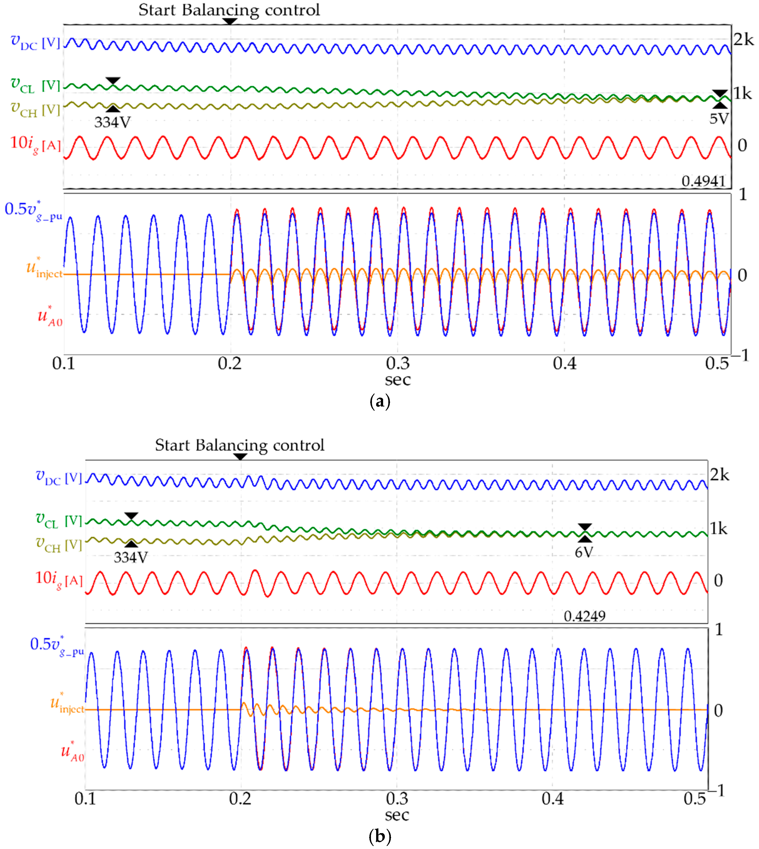
Figure 9 shows the simulation results for the dc-link capacitor voltage balancing control with the type of injection voltage under the same modulation index. In the simulation, the voltage difference between the upper and lower capacitor of the dc-link was enforced at about 334 V.
Figure 9a shows the simulation results of the dc-link capacitor voltage balancing control using distribution factor
μ. From the simulation results, each capacitor voltage
VCH and
VCL reached a balanced point at
t = 0.4941 s.
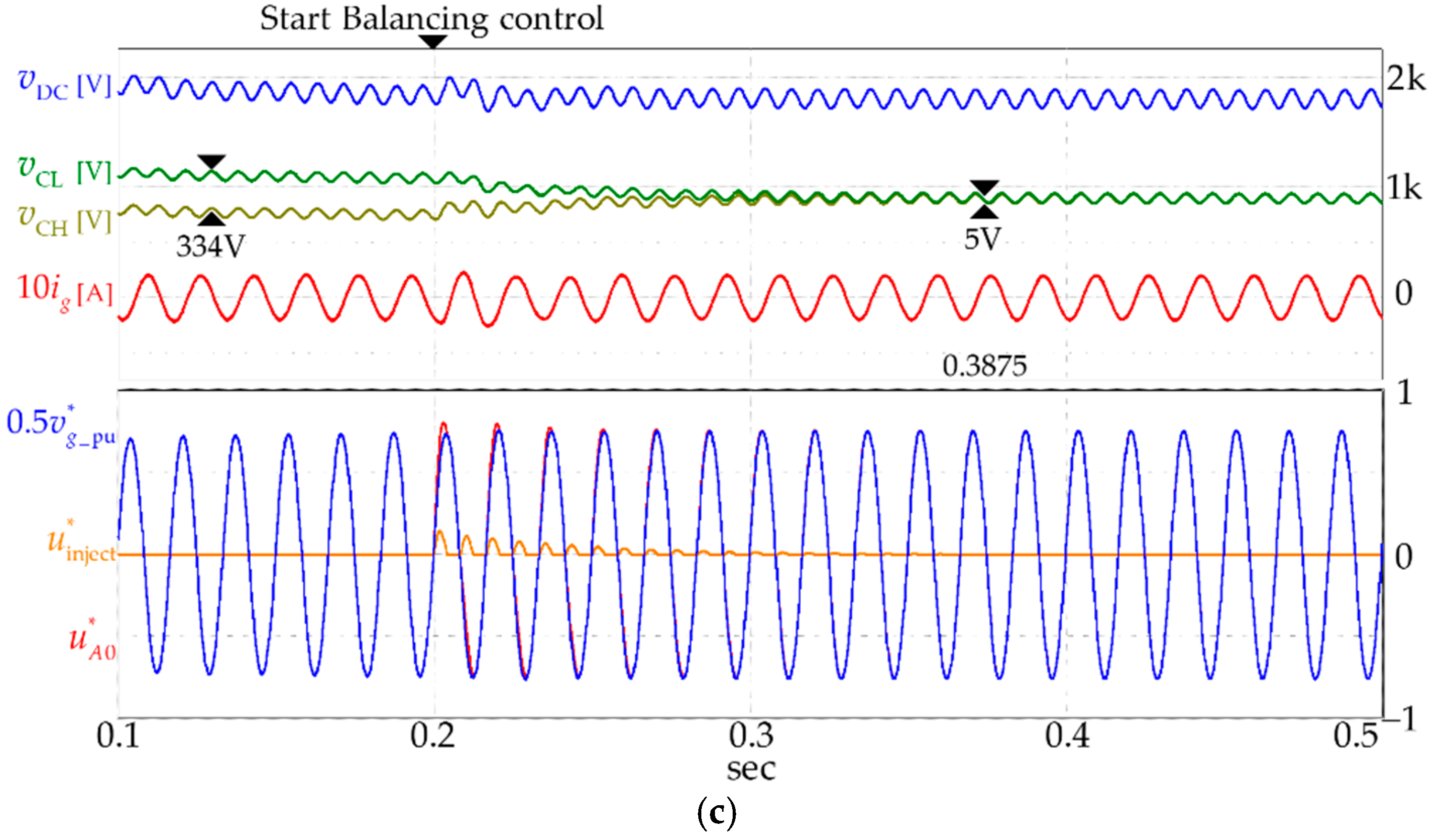
Figure 9b shows the simulation results when injecting a second-order harmonic signal into the modulation signal. In this case, each capacitor voltage
VCH and
VCL reached a balanced point at
t = 0.4249 s.
Figure 9c shows the simulation result when injecting the half-wave of a second-order harmonic signal into the modulation signal. In this case, the upper and lower capacitor voltage reached a balanced point at 0.3875 s. From the simulation results, the half-wave of the second-order harmonic signal injection method was better than other offset voltage injection methods.
Figure 10 shows a photograph of the experimental setup for a single-phase three-level NPC inverter used to verify the proposed method. The NPC inverter module consisted of two NPC half-bridges, a series filter inductor, and two electrolytic capacitors. For the test, a 6 kW resistive load was connected to the dc-link capacitor of the NPC inverter. The same system parameters for the NPC inverter were applied as in the previous simulation. A 1:6 transformer was connected to the output of the variac to obtain 943 V AC voltage. Each leg of the NPC inverter consisted of four MOSFETs and two clamping diodes. SiC MOSFETs, Cree’s C2M0040120D, and a SiC Schottky diode, Cree’s C4D20120D, were utilized for each leg. By adapting silicon carbide devices, the switching frequency can be higher than for silicon-based devices. When using a higher switching frequency, the physical size of the magnetic component for the NPC inverter can be reduced. Furthermore, a lower switching loss is expected than with silicon-based devices. Component specifications of the NPC inverter are shown in
Table 2. In order to measure the dc-link capacitor voltage and input current, a differential probe and a current probe were used. For each probe of the dc-link capacitor, PINTEK’s high voltage differential probe DP-50 was used. In addition, for input current, Lecroy’s current probe CP150 was used. The control structure of the NPC inverter contained a current controller for input current, a voltage controller for the dc-link capacitor voltage, and a voltage balance controller for the dc-ink capacitor voltage balance. For these controllers, a digital control board based on Texas Instruments’ TMS320F28335 was used, which was made in-laboratory. The phase voltage reference signal for the NPC inverter was generated by measuring the dc-link capacitor voltage and input current, and the injection signal for the dc-link capacitor voltage balance was calculated from the measured dc-link capacitor voltage and the phase angle of the grid. The NPC inverter regulated the AC voltage to DC voltage without the dc-link capacitor voltage imbalance caused by the generated phase voltage reference signal and injection signal.
In the above experimental setup, the experimental process was as follows: first, the AC input voltage was increased to 943 V under dc-link voltage control conditions for 1.8 kV dc-link voltage. Second, the dc-link capacitor voltage imbalance was enforced at about 100 V by operating an additional resistive load circuit, which was attached on the upper capacitor. At this time, the voltage difference should be suppressed by the voltage rating of the electrolytic capacitor. In addition, then, the adopting proposed method, dc-link voltage, separated capacitor voltage, and current distortion were observed intensively under unbalanced dc-link capacitor voltage.
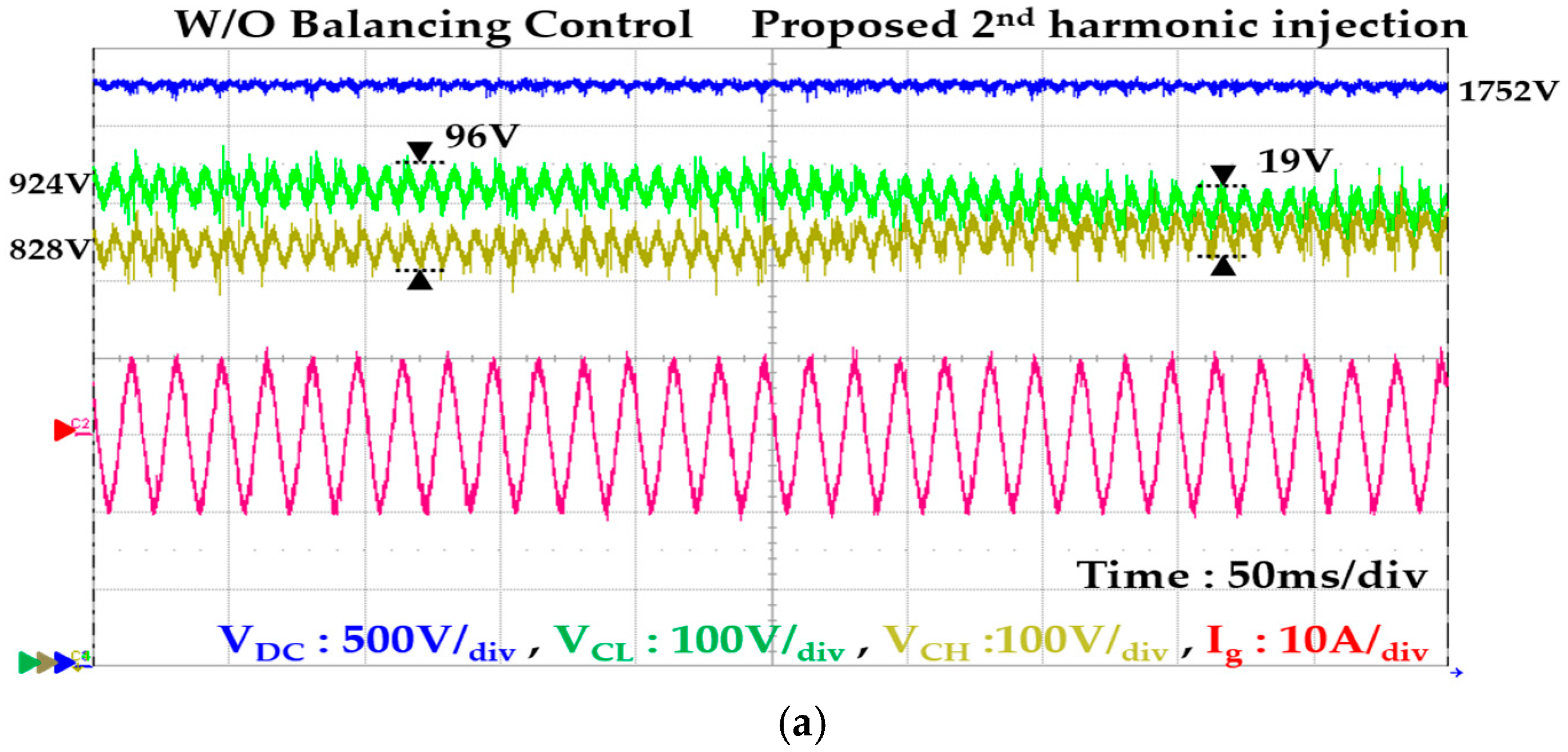
The experimental results when adopting the proposed method for dc-link capacitor voltage balance are presented in
Figure 11. As shown in
Figure 11a,b, the capacitor voltage difference was enforced at about 100 V. Before adopting the balancing control in
Figure 11a, the upper and lower capacitor voltage levels were measured as 828 V and 924 V, respectively. After adopting the proposed second-order harmonic injection method, the upper capacitor voltage level increased from 828 V to 869 V, and the lower capacitor voltage level decreased from 924 V to 887 V. In
Figure 11b, the other experimental result, the capacitor voltage difference was measured as 106 V. After adopting the proposed half-wave rectified second-order harmonic injection, the capacitor voltage difference decreased from 106 V to 9 V. At the beginning of the capacitor voltage balancing control, the line current
ig was instantaneously distorted, but this distortion disappeared within 50 ms as the upper and the lower capacitor voltage level became equal.
From the simulations and experimental results, the proposed capacitor voltage balancing control strategies of injecting the second-order harmonic signal and the half-wave of the second-order harmonic signal were effective for dc-link capacitor voltage balancing. Among these balancing methods, the method of injecting the half-wave signal into the modulation signal was faster, at about 50 ms, at achieving capacitor voltage balance than the injection of the full-wave signal of the second-order harmonic. However, in the case of input current ig, the full-wave injection method of the second-order harmonic had a lower distortion than the half-wave signal injection method as it seems that the synthesized pole voltage reference signal was distorted when the half cycle of the second-order harmonic signal had a negative polarity.


