Article

A Novel Reversal Γ-Shape Coupled Inductor High-Step AC-AC Converter

School of Electrical Engineering and Automation, Harbin Institute of Technology, No. 92, Xidazhi Street, Nangang District, Harbin 150001, China
*
Author to whom correspondence should be addressed.
Energies 2018, 11(10), 2733; https://doi.org/10.3390/en11102733
Submission received: 21 August 2018 / Revised: 23 September 2018 / Accepted: 25 September 2018 / Published: 12 October 2018

Abstract

:
This paper presents a novel reversal Γ-shape coupled inductor high-step AC-AC converter. This converter uses a reversal Γ-shape coupled inductor that consists of a two-winding coupled inductor for higher voltage gain. As the coupling inductance ratio is closer to 1 or the duty ratio is larger, the boosting capability of this converter is enhanced. The proposed converter has the following advantages: first, it can realize a continuous input current. Second, the input and output voltage have a common ground in the proposed converter. Apart from these features, the proposed topology has a higher voltage gain with a lower voltage stress on switches and the proposed topology has low cost, and a simple configuration and control scheme. The gain of the proposed high-step AC-AC converter is determined by more variables. Thus, when designing the converter there are more options to meet different requirements. The principle of operation is described and discussed in this paper. In addition, the operating performance is illustrated and estimated based on simulation and experimental results.

1. Introduction

In recent years, high-voltage AC-AC boost converters are attracting more and more attention. In AC power conversion systems, direct PWM AC-AC converters [1,2], indirect AC-AC converters [3] and matrix converters based on switching device [4] have been widely used. The back-to-back dc-link converters have the disadvantages of the power system pollution caused by the diode-rectifier. The disadvantage of matrix converters is their lower voltage ratio. The two converters mentioned above also have complex structures and commutation strategies. Direct PWM AC-AC converters have merits such as single-stage conversion, simpler topology, easier control, higher efficiency, smaller size, lower cost and lower in-line current harmonics.
Since the end of the last century, more and more DC-DC converters were proposed based on various impedance network layouts [5,6]. In theory, a direct PWM AC-AC converter could be obtained from a DC-DC topology by replacing all unidirectional devices with bidirectional switches [7]. The converters based on impedance have some advantages as increasing the voltage gain, adding more flexible options in the design and a larger adjustment range in the gain adjustment. Traditional single-phase Z-source AC-AC uses a consistent style converters can provide a larger range of output voltage in buck–boost mode, by reversing or maintaining the phase angle [8,9]. However, the main drawback of conventional voltage-fed ZSACs [10] is that the ground in the input and output voltages is not shared. Hence, the feature that the output voltage reverses or maintains its phase angle with the input voltage is not supported well. The authors in [11,12] used direct PWM AC-AC converters to overcome voltage sags and swells as static VAR compensators in power systems. The performance of AC-AC converters can be improved significantly using safe-commutation strategy in switching with PWM control as presented in [13]. A class of single phase PWM AC-AC power converters with simple topologies have been presented in [14]. These include buck, boost, buck–boost, and Cuk converters. Z-source converters applied to DC-AC inverters and ac–ac converters have recently been proposed in [8] and [15,16,17,18]. Trans Z-source inverters have recently been proposed to improve the voltage gain using coupled inductors [18,19]. A quasi-Z-source converter has been presented in [17,20]. The proposed converter utilizes two winding coupled inductors or a two-winding transformer. The main merits of the Γ-source converter can be summarized as continuous input current, common ground, simple configuration and control scheme, realizing higher voltage gains with a lower voltage stress on switches, having more adjustments when changing its gain and having more design options to meet its performance requirements.
The designed novel reversal Γ-shape coupled inductor high-step converter based on the Γ-source impedance network. The Γ-source converter in this paper is showing in Figure 1 below. As we can see from Figure 1, the proposed converter consists of a coupled inductor (LM), inductor (L), switches (S1, S2, S3, S4, S5 and S6), capacitors (C1, Cc and Co) and load (R). The numbers of turns of the two windings of this coupled inductor are N1 and N2. The unique characteristic of this converter is that the closer the turns ratio (N = N1:N2) of the two windings (N1 and N2) is to 1, the more the boosting capability of this converter is enhanced. Therefore, this converter still has better boosting capability at a lower design cost and high engineering application value. To improve the voltage gain and decrease the voltage stress on switches, a capacitor clamping unit has been used in the proposed converter.

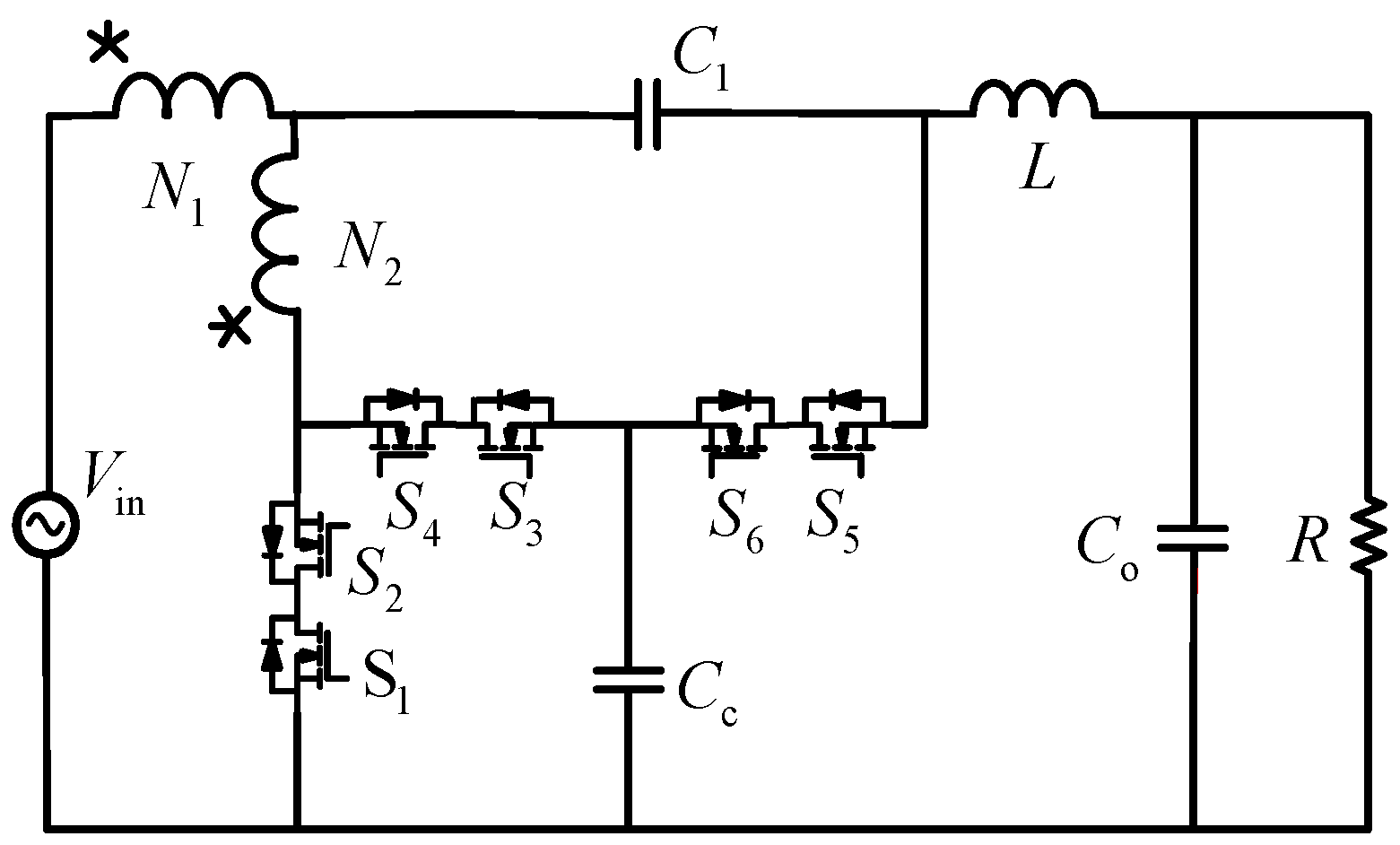
2. Study of the Proposed Reversal Γ-Source Ac-Ac Converter

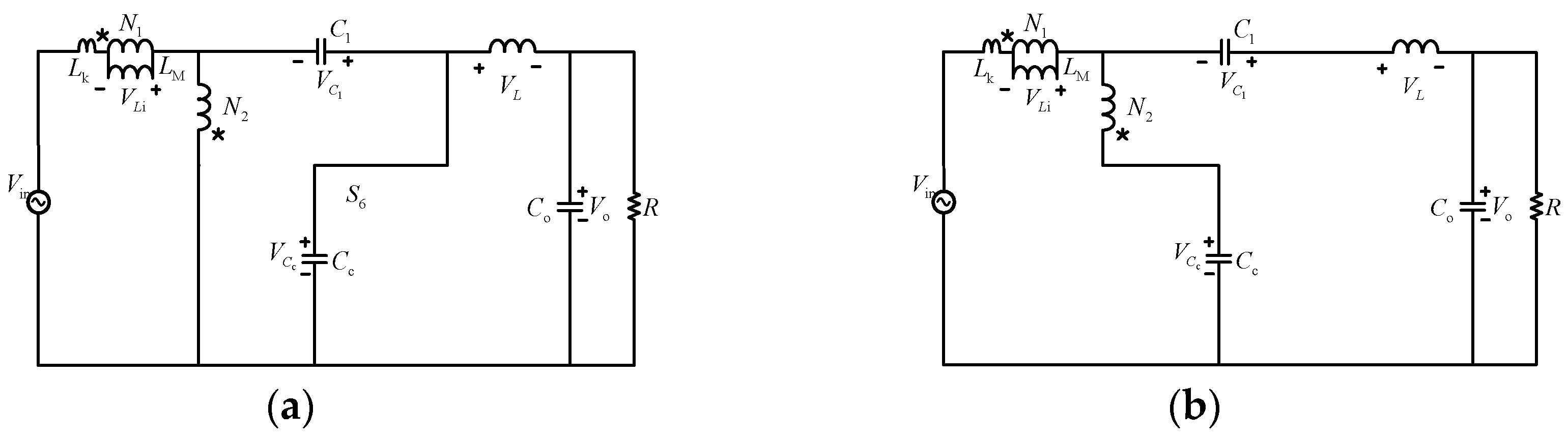
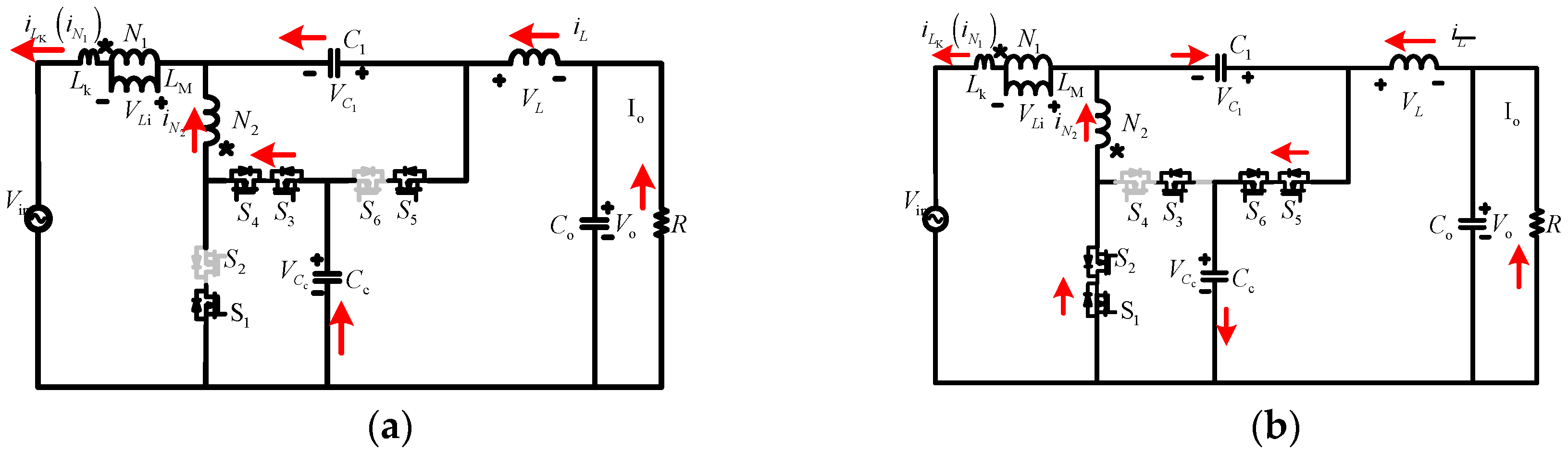
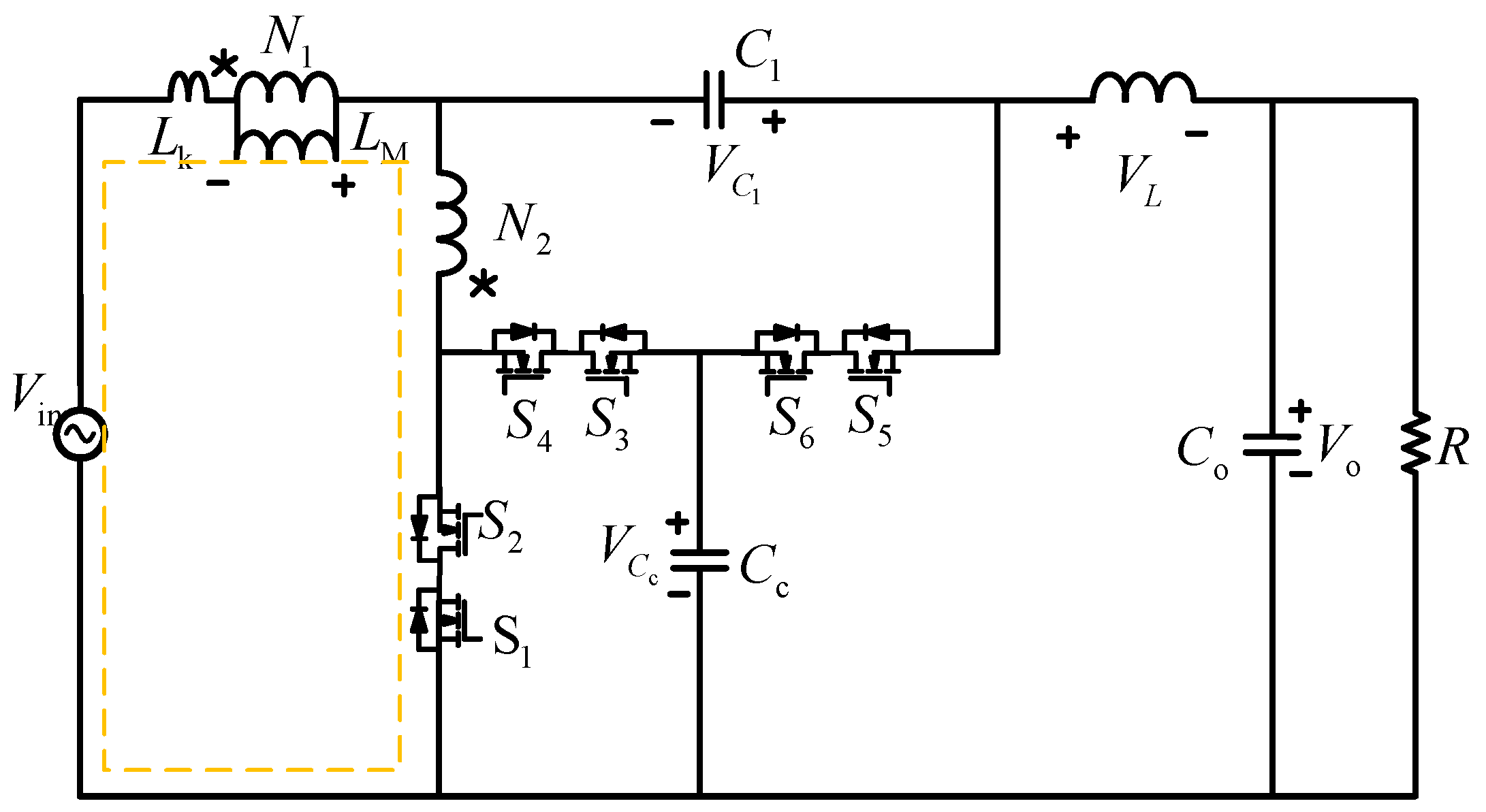
2.1. Circuit Analysis

In this section, the topology proposed in Figure 1 will be analyzed in details. The equivalent circuit of the presented converter is shown in Figure 2. It is clearly seen that the coupled inductor is modeled as a magnetizing inductance L M , a leakage inductance L K , and an ideal transformer. For easier analysis of the circuit, we make some assumptions as follows:
(1)
Assuming that the capacitors ( C 1 , C c and C o ) values are large enough, the voltage across them is fixed over a period.
(2)
All power devices in the experiment were ideal devices.
(3)
Define L M / ( L M + L K ) as the coupling coefficient K of the coupled inductor and define N 1 / N 2 as the turn ratio N of the coupled inductor.
Using these definitions, the proposed converter in shoot through and non-shoot through states were shown in Figure 3. Time in the state of Figure 3a in one cycle is written as DT and the time in the state of Figure 3b in one cycle is written as (1-D)T, in which D is the duty cycle and T is the cycle time.
In shoot-through state as shown in Figure 3a, the time interval in this state is DT. Accordingly, the state equations can be derived as:
{ V o + V L V C 2 = 0 V C C + V L M + V C 1 V i n = 0 V i n N 1 + N 2 N 1 L L M = 0 I C o I L + V o R = 0 I C c I L + I C 1 = 0 I C 1 + N 1 N 2 N 2 I L M = 0
In the non-through state as shown in Figure 3b, the time interval in this state is (1-D)T. Accordingly, the state equations can be derived as:
{ V C C + N 1 + N 2 N 1 V L M V i n = 0 V i n V L M V C 1 V L V o = 0 I C o I L + V o R = 0 I C 1 + N 1 N 2 N 2 I L M = 0 I C C + N 1 N 2 I L M = 0
In the above formula, Vo is the output voltage, I L M is the current flowing through the inductor L M , I C o is the current flowing through capacitor C o , I C 1 is the current flowing through capacitor C 1 , I C c is the current flowing through capacitor C c , V L M is the voltage across inductor L M , V C 1 is the voltage across the capacitor C 1 , V C c is the voltage across the capacitor C c .
In one cycle, the average equation is as follows:
0 D T V L M d t + D T T V L M d t = 0
Finally, based on (1)–(3), the voltage gain of the proposed reversal Γ-shape coupled inductor AC-AC converter can be computed as:
M = N D 2 N + D K ( 1 D ) ( K N )
In the above formula, M is the voltage gain.
Figure 4 shows the relationship between voltage gain and duty cycle at different coupling coefficients.
It can be obtained from Equation (4) that as the coupling coefficient K increases, the voltage gain of the proposed converter increases. If the coupling coefficient K is infinitely close to 1, the equation can be written as follows:
M = N D 2 N + D ( 1 D ) ( 1 N )
Figure 5 reflects the effect of the turn ratio N on the proposed converter gain. It can be derived from Equations (4) and (5) that the voltage gain would increase while the turns ratio is close to 1. This converter reduces the manufacturing cost while increasing the voltage gain. It also can simplify the structural design.

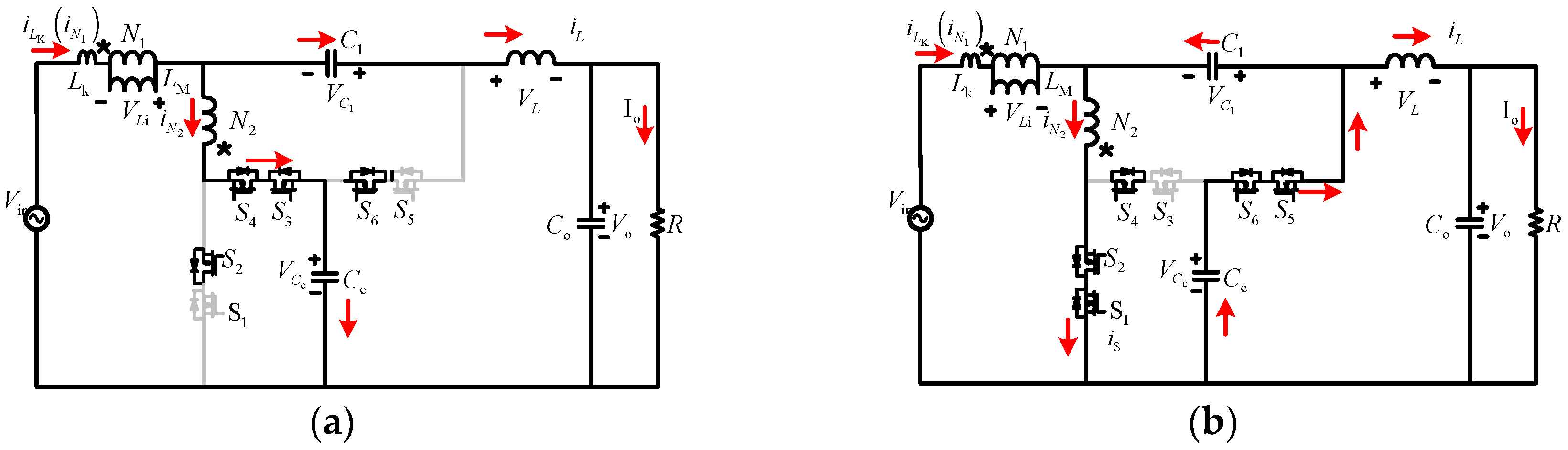
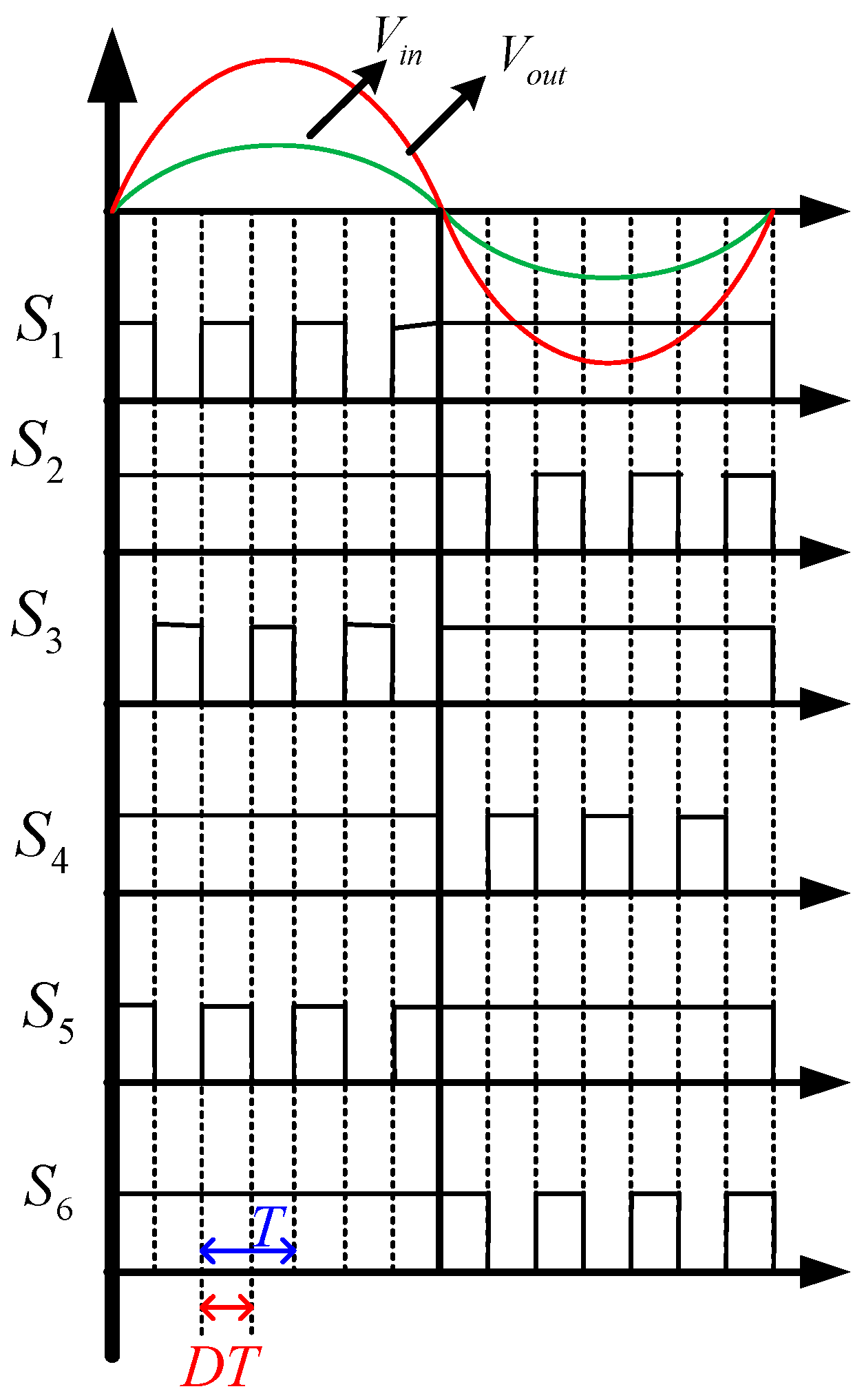
2.2. Commutation Study of the Proposed Converter

As shown in Figure 2, to implement a bidirectional switch, the two MOSFETs are linked with a common emitter, using a safety commutation strategy to prevent the damage of current and voltage spikes on switches.
The operation states in “in-phase boost mode” when Vin > 0 is shown in Figure 6. Switches S2, S4 and S6 are completely turned ON, while S1, S2 and S3 are switched complementary in high frequency with a small dead time between them.
In non-shoot through state, as shown in Figure 6a, the switch S1 and S5 are turned off. The energy of the inductor N2 stares to transmit to the clamped capacitor Cc. The input source Vin, inductor N1, and capacitor C1 are connected in series to provide the energy to load and capacitor Co. And the magnitude of the inductor L current would increase during this state.
In shoot-through state, as shown in Figure 6b, switches S1 and S5 are turned ON. The voltage source Vin charges the input inductor LM, thus the magnitude of the LM current would increase gradually. The secondary inductor N2 and capacitor Cc are connected in series to charge the capacitor C1. During this mode the energy of the load R is supplied by the output capacitor Co and inductor L.
When the Vin < 0, the analysis method is like that Vin > 0. And operation states of the converter when Vin < 0 are shown in Figure 7. During this period the switches S1, S3 and S5 are turned ON, while S2, S4 and S6 are switched complementary in high frequency. The gate voltage signals of switches are shown in Figure 8.

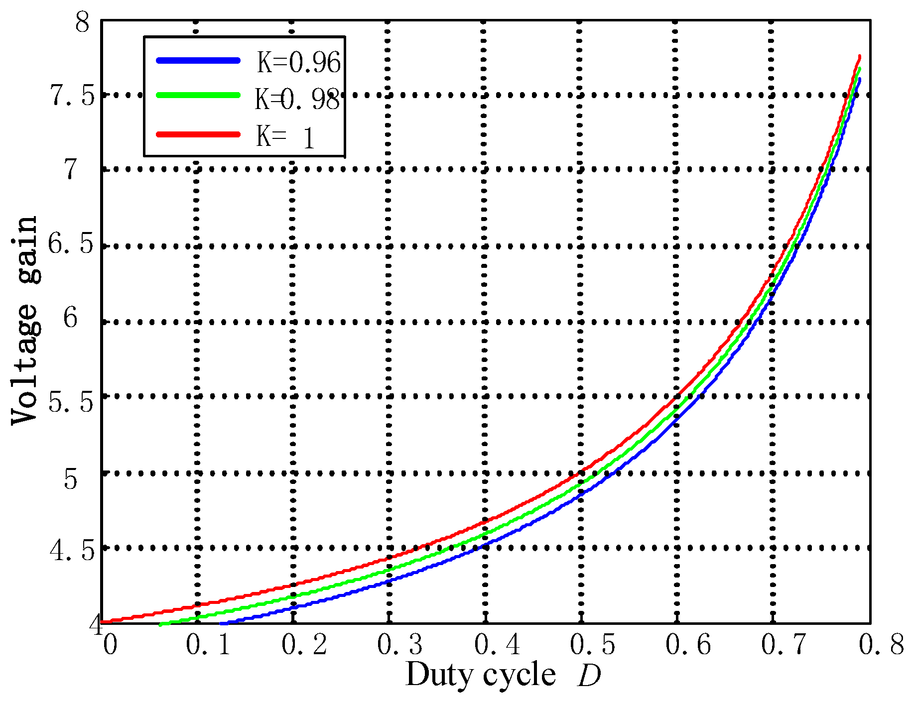
2.3. Parameter Design

The coupled inductor parameters of the novel reversal Γ-shape coupled inductor converter has been calculated as follows. In the state of Figure 3b, the voltage of the coupled inductor L M could be calculated as K N N + K V i n :
u L M = L M d i d t
According to the voltage equation of inductor (6), the following equation can be derived:
L M u L M d t d i
As we can see from the Figure 9, the following equation can be obtained:
u L M = N 1 N 1 + N 2 V i n
Thus, Equation (9) can be derived:
L M N 1 N 1 + N 2 | V i n | d t d i
Replacing d i with Δ i L M , we can replace d t with D T , so, the following equation can be obtained:
L M N N + 1 D T | V i n | Δ i L M
Considering the range of current ripple is Δ i m x % I L M , Equation (11) can be derived:
L M N N + 1 D T | V i n | x % I L M
Similar to the above deduction process, we could determine the parameters of the capacitor C c . The results can be obtained as:
C c = D T | i L M | Δ V C C
Assume that the voltage ripple coefficient of the capacitor is m % , the equation of the value range of the capacitor parameters can be described as:
C c D T | i L M | m % V C C
By the same method, the equation of C 1 can be written as:
C 1 N 1 N D T | i L M | m % V C 1
Finally, the parameter design of the output filter is as follows. The parameter of the output filter inductor is calculated as follows [21]:
L = ε R 2 π f c
and, the expression of ε is as follows:
ε = 1 R L C
Moreover, the parameter of the output filter capacitor could be derived as:
C o = 1 2 π f c ε R
f c represents the cutoff frequency of the output filter. R represents the load resistance. And L represents filter inductor. ε is greater than 0.5 and less than 0.8. The ε is select as 0.6. The efficiency of the filter will reduce when ε is too large or too small:
V S 1 = V C c = ( 2 N D N 1 ) N D + D N 1 V i n
V S 3 = ( N 1 ) ( N + 1 ) ( 1 D ) V i n
According to the above equations, we can obtain the voltage of capacitor C1 and Cc as follows:
V C 1 = 2 D N 1 D N D N + 1 V i n
V C C = 2 N D N 1 D N + D N 1 V i n

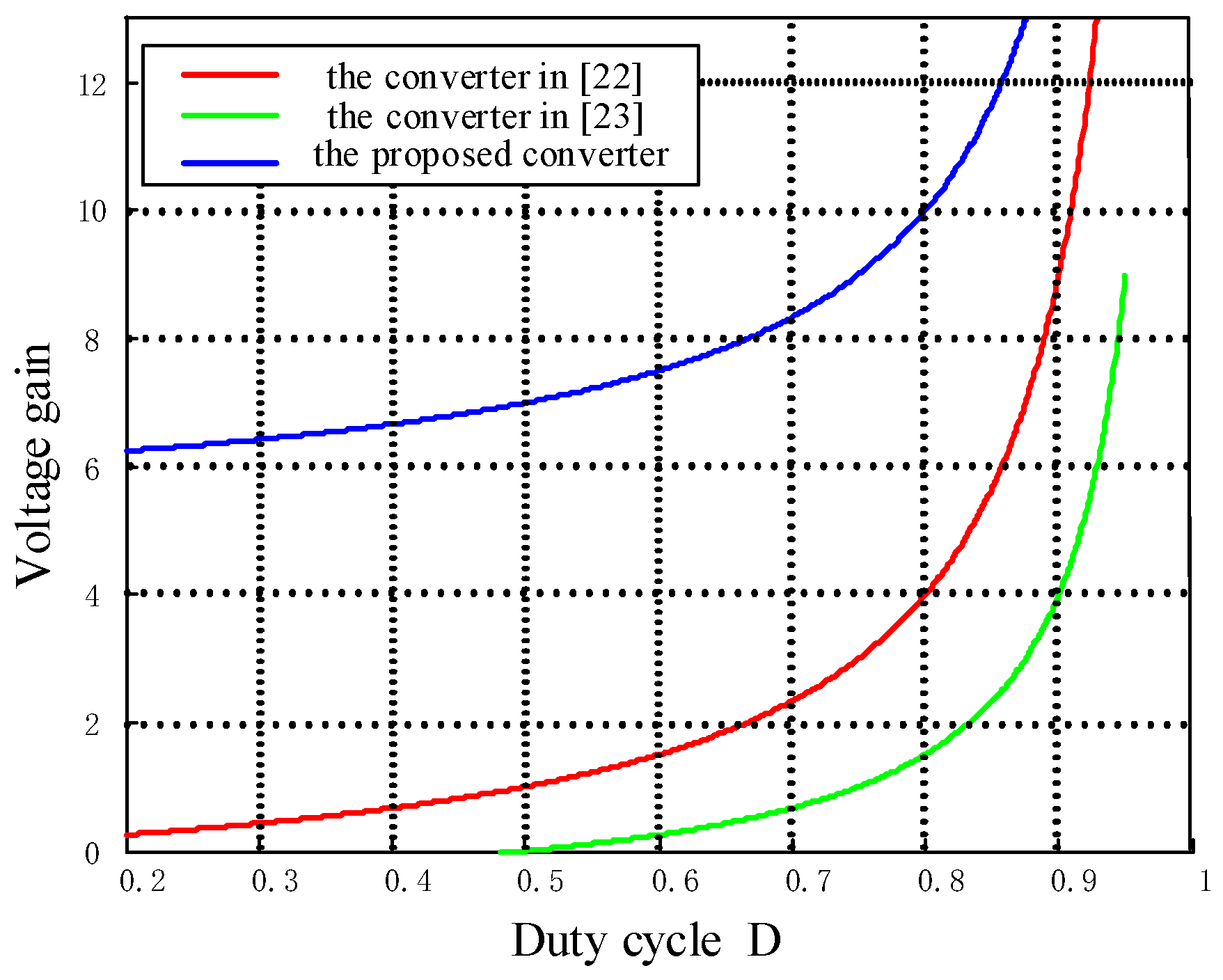
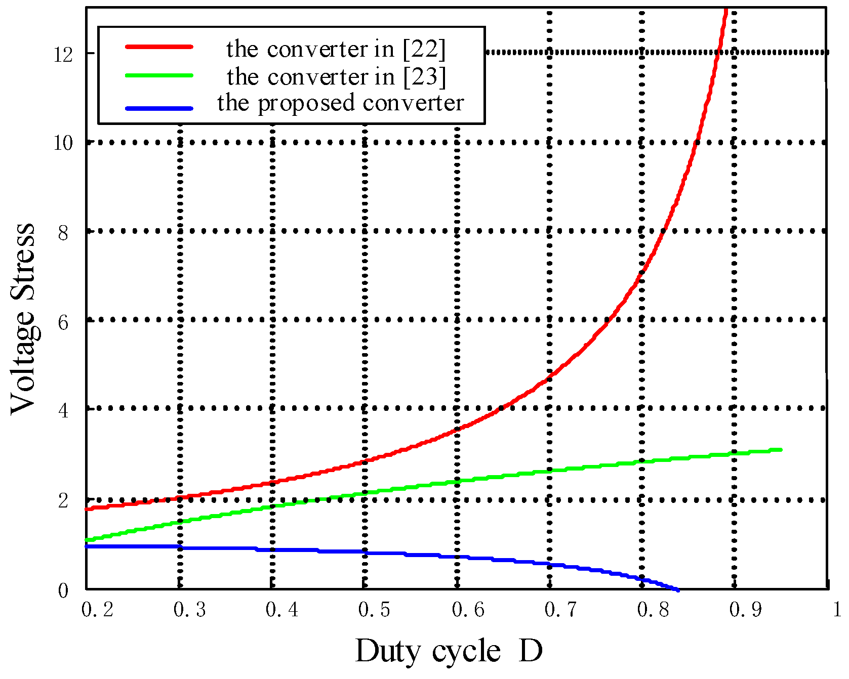
2.4. Proposed Converter Versus Other

Besides the proposed converters based on reversal Γ-shape coupled inductor, there are many converters that have been proposed in previous papers. Detailed related introductions can be found in the respective references.
From Table 1, it could be known clearly that the voltage stresses of switches in the proposed converter are far lower than output voltages, therefore low-voltage-rated power switches can be used in the proposed converter. Apart from this, as we can see from Table 1, in the proposed Γ-shape coupled inductor converters, when the turns ratio comes close to 1, the gain become larger.
When the coupled inductor turns ratio is 1.5, the graphs of Figure 10 and Figure 11 are obtained. Figure 10 and Figure 11 show the output voltage gains and voltage stress of MOSFETs. Figure 10 and Figure 11 show that the voltage gain of proposed reversal Γ-shape coupled inductor converter is higher than that of previous topologies in [22,23] while the voltage stresses are lower. Figure 10 shows that the proposed reversal Γ-shape coupled inductor converter has a higher voltage gain than the converters in [22,23] under the same circumstances. Figure 11 shows that the proposed reversal Γ-shape coupled inductor converter has lower voltage stress than the converters in [22,23] under the same circumstances.

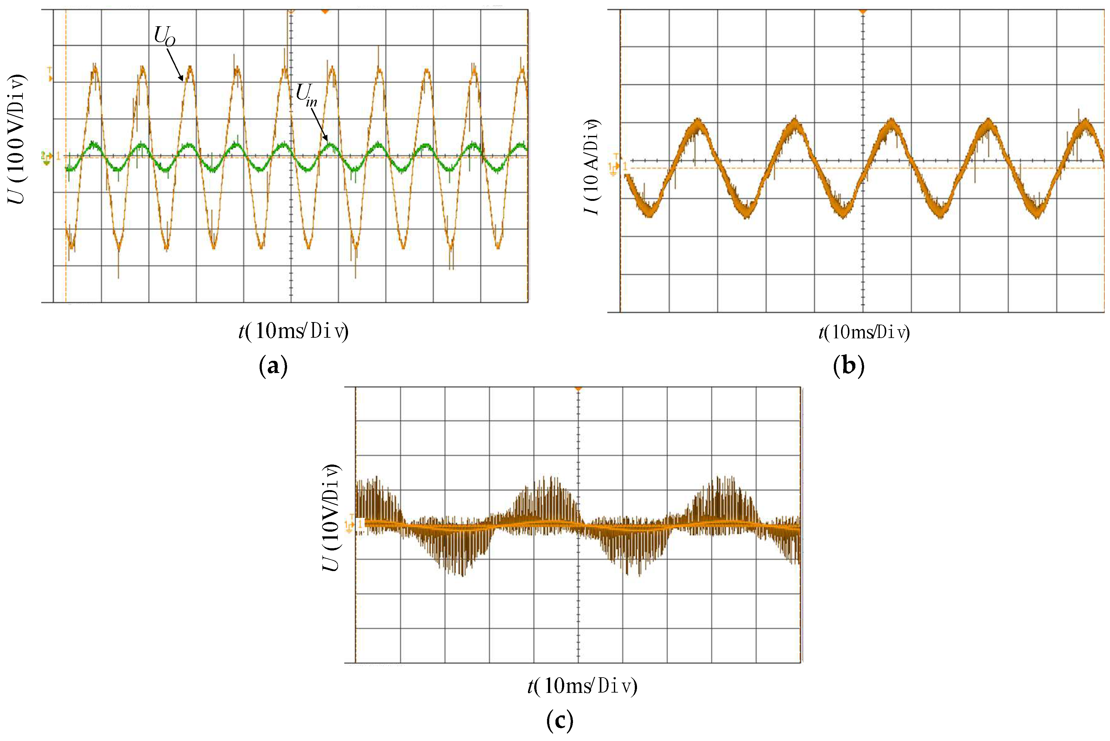
3. Experimental Verifications

To verify the performances of the proposed reversal Γ-shape coupled inductor converter, experiments were carried out according to the experimental parameters given in Table 2. Experimental verification of the proposed novel topology is achieved and controlled using a digital signal processor (TMS320F28335). Switching frequency is set at 20 kHz. The duty cycle is 0.72. The tested condition and experimental parameters are shown in Table 2.
The experimental results of the novel reversal Γ-shape coupled inductor converter have been illustrated in Figure 12. Figure 12a shows the input and output voltages of the proposed reversal Γ-shape coupled inductor converter. In Figure 12a, the green waveform is the input voltage waveform and the yellow waveform is the output voltage waveform.
As we can see from the result, the input voltage amplitude of the proposed converter is 30 V and the output voltage amplitude of the proposed converter is about 250 V. Both the input and output voltages are sinusoidal. The voltage gain of the proposed converter was verified. The input current has been shown in Figure 12b which is also a sinusoidal waveform. Figure 12c shows the voltage stress of the switch S1. As can be seen from Figure 12c, the maximum voltage stress on switch S1 is about 13 V. The experimental results agree with the calculation, which verifies the validity of our theoretical analysis.

4. Conclusions

In this article, a novel reversal Γ-shape coupled inductor high-step AC-AC converter is presented. The proposed converter utilizes a safe commutation strategy to avoid voltage and current spikes. The modulation strategy, analysis of operation states and parameter design are introduced. The input voltage and output voltage share the same ground, which is beneficial for reducing the input current harmonics. As the coupling inductance ratio is closer to 1 or the duty ratio is larger, the voltage gain of this converter is enhanced. This exclusive feature is beneficial to reduce the structural cost of the converter while achieving high voltage gain. The gain of the proposed high-step AC-AC converter is determined by more variables. Thus, when designing the converter there are more options to meet different requirements. Finally, the experimental results prove the correctness of the theoretical analysis. The proposed converter has better performance that other proposed devices.

Author Contributions

Writing—original draft, X.Z.; Writing—review & editing, H.L.

Funding

This research was funded by the National Natural Science Foundation of China (51777043), State Key Laboratory of Electrical Insulation and Power Equipment (EIPE18208), and the Postdoctoral Science-Research Developmental Foundation of Heilongjiang Province (LHB-Q12086).

Conflicts of Interest

The authors declare no conflict of interest.

References

  1. He, L.Z.; Nai, J.X.; Zhang, J.H. Single-phase safe-commutation trans-z-source AC-AC converter with continuous input current. IEEE Trans. Ind. Electron. 2018, 65, 5135–5145. [Google Scholar] [CrossRef]
  2. Zhao, Z.Y.; Yang, J.; Zhu, Q.; Wang, C.S.; Jian, F. A direct AC-AC converter for electronic power transformer based on energy injection control. In Proceedings of the 2016 2nd International Conference on Control Science and Systems Engineering (ICCSSE), Singapore, 27–29 July 2016; pp. 212–216. [Google Scholar] [CrossRef]
  3. Albreem, M.A.M.; Naser, H.T.A.; Abofares, M.E.A. Design of indirect AC-AC converter based on linear controller for power systems. In Proceedings of the 2016 International Conference on Advances in Electrical, Electronic and Systems Engineering (ICAEES), Putrajaya, Malaysia, 14–16 November 2016; pp. 500–505. [Google Scholar] [CrossRef]
  4. Fedyczak, Z.; Szczesniak, P. Matrix-reactance frequency converters using an low frequency transfer matrix modulation method. Electr. Power Syst. Res. 2012, 83, 91–103. [Google Scholar] [CrossRef]
  5. Liu, Y.S.; Abu-Rub, H.; Ge, B.; Blaabjerg, F.; Ellabban, O.; Loh, P.C. Impedance Source Power Electronic Converters; Wiley: Hoboken, NJ, USA, 2016. [Google Scholar]
  6. Siwakoti, Y.P.; Peng, F.Z.; Blaabjerg, F.; Loh, P.C.; Town, G.E. Impedance-source networks for electric power conversion part I: A topological review. IEEE Trans. Power Electron. 2015, 30, 699–716. [Google Scholar] [CrossRef]
  7. Fedyczak, Z.; Strzelecki, R.M.; Sozanski, K. Review of three-phase AC/AC semiconductor transformer topologies and applications. In Proceedings of the Symposium on Power Electronics, Electrical Drives, Automation & Motion, SPEEDAM’02, Ravello, Italy, 11–14 June 2002. [Google Scholar]
  8. Fang, X.P.; Qian, Z.M.; Peng, F.Z. Single-phase Z-source PWM ACAC converters. IEEE Power Electron. Lett. 2005, 3, 121–124. [Google Scholar] [CrossRef]
  9. Tang, Y.; Xie, S.J.; Zhang, C.H. Z-source AC-AC converters solving commutation problem. IEEE Trans. Power Electron. 2007, 22, 2146–2154. [Google Scholar] [CrossRef]
  10. Subramanian, S.; Mishra, M.K. Interphase AC-AC topology for voltage sag supporter. IEEE Trans. Power Electron. 2009, 25, 514–518. [Google Scholar] [CrossRef]
  11. Divan, D.M.; Sastry, J. Voltage synthesis using dual virtual quadrature sources—A new concept in ac power conversion. IEEE Trans. Power Electron. 2008, 23, 3004–3013. [Google Scholar] [CrossRef]
  12. Nguyen, M.K.; Jung, Y.G.; Lim, Y.C.; Kim, Y.M. A single-phase Z-source buck-boost matrix converter. IEEE Trans. Power Electron. 2010, 25, 453–462. [Google Scholar] [CrossRef]
  13. Nguyen, M.-K.; Jung, Y.-G.; Lim, Y.-C. Single-phase quasi-Z-source AC-AC converter with safe-commutation strategy. In Proceedings of the 2010 International Power Electronics Conference—ECCE ASIA, Sapporo, Japan, 21–24 June 2010; pp. 562–566. [Google Scholar] [CrossRef]
  14. Peng, F.Z.; Chen, L.; Zhang, F. Simple topologies of PWM AC-AC converters. IEEE Power Electron. Lett. 2003, 1, 10–13. [Google Scholar] [CrossRef]
  15. Stala, R.; Pirog, S.; Mondzik, A.; Baszynski, M.; Penczek, A.; Czekonski, J.; Gasiorek, S. Results of investigation of multicell converters with balancing circuit. Part II. IEEE Trans. Ind. Electron. 2009, 56, 2620–2628. [Google Scholar] [CrossRef]
  16. Wilkinson, R.H.; Meynard, T.A.; Mouton, H.T. Natural balance of multicell converters: The general case. IEEE Trans. Power Electron. 2006, 21, 1658–1666. [Google Scholar] [CrossRef]
  17. Nguyen, M.K.; Jung, Y.G.; Lim, Y.C. Single-phase AC-AC converter based on quasi-Z-source topology. IEEE Trans. Power Electron. 2010, 25, 2200–2210. [Google Scholar] [CrossRef]
  18. Strzelecki, R.; Adamowicz, M.; Strzelecka, N.; Bury, W. New type T-source inverter. In Proceedings of the 2009 Compatibility and Power Electronics, Badajoz, Spain, 20–22 May 2009; pp. 191–195. [Google Scholar]
  19. Qian, W.; Peng, F.Z.; Cha, H. Trans-Z-source inverters. IEEE Trans. Power Electron. 2011, 26, 3453–3463. [Google Scholar] [CrossRef]
  20. Anderson, J.; Peng, F.Z. Four quasi-Z-source inverters. In Proceedings of the 2008 IEEE Power Electronics Specialists Conference, Rhodes, Greece, 15–19 June 2008; pp. 2743–2749. [Google Scholar]
  21. Chen, D.L. The Uni-polarity phase-shifted controlled buck mode AC/AC converters with high frequency link. In Proceedings of the 2007 IEEE Power Electronics Specialists Conference, Orlando, FL, USA, 17–21 June 2007; pp. 471–476. [Google Scholar] [CrossRef]
  22. Khan, A.A.; Cha, H.; Ahmed, H.F. An improved single-phase direct pwm inverting buck–boost AC-AC converter. IEEE Trans. Ind. Electron. 2016, 63, 5384–5393. [Google Scholar] [CrossRef]
  23. Sharifi, S.; Jahani, F.; Monfared, M. Direct single phase AC-AC converters based on novel series impedance networks. IEEE Trans. Power Electron. 2018, 33, 10380–10389. [Google Scholar] [CrossRef]
Figure 1. Proposed reversal Γ-shape coupled inductor AC-AC converter.
Energies 11 02733 g001
Figure 2. Equivalent circuit of the proposed converter.
Energies 11 02733 g002
Figure 3. Two steady-states of the proposed converter: (a) shoot-through state; (b) non-shoot through state.
Energies 11 02733 g003
Figure 4. Effect of K on the voltage gain when N = 2.
Energies 11 02733 g004
Figure 5. Effect of N on voltage gain.
Energies 11 02733 g005
Figure 6. Operation states of the converter when V i n > 0: (a) Non-shoot through state; (b) Shoot through state.
Energies 11 02733 g006
Figure 7. Operation states of the converter when V i n < 0: (a) Non-shoot through state; (b) Shoot through state.
Energies 11 02733 g007
Figure 8. Switching strategy of the proposed converter.
Energies 11 02733 g008
Figure 9. Equivalent circuit used to calculate LM.
Energies 11 02733 g009
Figure 10. Comparison of voltage gain of converters.
Energies 11 02733 g010
Figure 11. Comparison of the maximum switches voltage stresses of converters.
Energies 11 02733 g011
Figure 12. Experimental results based on an R load (D = 0.72, N = 1.5): (a) Input and output voltage; (b) Input current; (c) Voltage of the S1.
Energies 11 02733 g012
Table 1. Governing equations of the existing converters and the proposed converter.
TopologyVoltage GainMaximum Voltage Stress of Switches
Converter in [22] D 1 D 2 V i n 1 D
Converter in [23] 1 N + D ( 1 D ) 2 ( 9 D 2 + 1 ) V i n 2 D ( 1 + D )
The proposed converter N D 2 N + D ( 1 D ) ( 1 N ) V S 1 , 2 = ( 2 N D N 1 ) N D + D N 1 V i n
V S 3 , 4 = ( N 1 ) ( N + 1 ) ( 1 D ) V i n
V S 5 , 6 = ( 2 D ) N D + D N 1 V i n
Table 2. Experimental parameters.
ComponentsParametersComponentsParameters
Maximum output power P250 WInductor L220 μ H
Input voltage Vin30 VInductor L1 mH
Output voltage Vo250 VC1 (Capacitor)4.7 μ F
Switching frequency fs20 kHzCc (Capacitor)4.7 μ F
Turns ratio n2/n1 of coupled inductor N1.5Co (Capacitor)20 μ F
Inductor L145 μ H Power MOSFET QIRFP 250 N

