Abstract
The application of constant power control and inclusion of energy storage in grid-connected photovoltaic (PV) energy systems may increase the use of two-stage system structures composed of DC–DC-converter-interfaced PV generator and grid-connected inverter connected in cascade. A typical PV-generator-interfacing DC–DC converter is a boost-power-stage converter. The renewable energy system may operate in three different operation modes—grid-forming, grid-feeding, and grid-supporting modes. In the last two operation modes, the outmost feedback loops are taken from the input terminal of the associated power electronic converters, which usually does not pose stability problems in terms of their input sources. In the grid-forming operation mode, the outmost feedback loops have to be connected to the output terminal of the associated power electronic converters, and hence the input terminal will behave as a negative incremental resistor at low frequencies. This property will limit the operation of the PV interfacing converter in either the constant voltage or constant current region of the PV generator for ensuring stable operation. The boost-power-stage converter can be applied as a voltage or current-fed converter limiting the stable operation region accordingly. The investigations of this paper show explicitly that only the voltage-fed mode would provide feasible dynamic and stability properties as a viable interfacing converter.
1. Introduction
Renewable energy systems are able to operate in three different operation modes—grid-feeding (Figure 1a), grid-supporting (Figure 1a), and grid-forming (Figure 1b) modes [1,2]—as well as transitioning between the modes smoothly [3]. The utility-scale photovoltaic (PV) energy systems are usually comprised of a single-stage system, where the inverter will take care of both the PV generator and grid integration duties. The requirement of coordinated constant power or power curtailment operation mode [4,5,6], as well as the power fluctuation control by means of energy storage facilities [7], may eventually change the PV system topology into a two-stage system, where a DC–DC converter takes care of the PV-generator interfacing duties, and the inverter takes care of the grid-interfacing duties, respectively. The PV-generator-interfacing DC–DC converter is typically a boost-power-stage converter [4], which is implemented by adding a capacitor at the input terminal of the conventional (i.e., voltage-fed) boost converter for satisfying the terminal constraints stipulated by the PV generator [8].
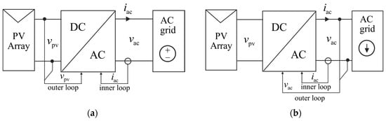
Figure 1.
Operation modes of a single-stage grid-connected PV energy system: (a) grid-feeding/supporting mode; (b) grid-forming mode.
It is well known that the PV generator is a highly nonlinear current source [8,9,10,11] containing basically two distinct operation regions based on the behavior of its I–V curve (Figure 2): a constant current region (CCR) at voltages less than the maximum power point (MPP) voltage, and a constant voltage region (CVR) at voltages higher than the MPP voltage. If considering the PV generator from its P–V curve point of view, an additional region appears in the vicinity of the MPP, which can be named the constant power region (CPR), as is also clearly visible in Figure 2. The regions are categorized based on the variable, which stays practically constant within the named region. It is also well known that the PV generator significantly affects the dynamics of the PV-interfacing converter through its low-frequency dynamic resistance (), which has similar resistance behavior to the named I–V-curve-based electrical sources [8]. As a summary of the above region definitions, it can be stated that in CCR, is rather high and stays rather constant; in CVR, is rather small and stays constant; and in CPR, , and stays constant, as shown in more detail in Section 3.
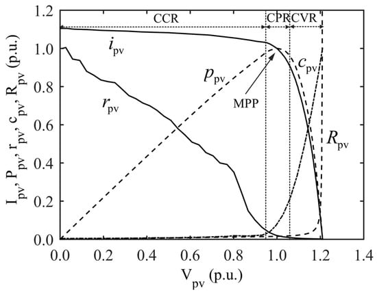
Figure 2.
Normalized behavior of the Ipv, Ppv, rpv, Rpv, and cpv with respect to Vpv when the operating point is varied. The normalization is carried out in such a manner that Ipv and Ppv are divided by their MPP values, rpv by its maximum value of , Rpv by , and cpv by its maximum value of .
The dynamic changes in the interfacing converter are induced by the behavior of the ratio of the dynamic and static () resistances of the PV generator [8]. At the MPP, the ratio equals unity [10], in CCR, , and in CVR, , respectively. The environmental conditions over the surface of the PV generator, such as clouds passing over or shadows caused by building structures as well as nearby trees and flagpoles, may cause shading of part of the PV-generator surface. The shading will cause multiple MPPs and thus multiple operational regions (i.e., CCRs and CVRs) to appear as demonstrated in [11], where the dynamic resistance () and capacitance () behave similarly in each region, as discussed above and shown in Figure 2 in the case of a single MPP. At every MPP, the corresponding dynamic and static resistances are equal [10].
When the PV energy system operates in grid-feeding or grid-supporting modes (Figure 1a), the outmost feedback loops have to be taken from the input terminals of the corresponding power electronic converters [2]. The input dynamics of the converter very seldom contains such control-related anomalies such as e.g., low-frequency right-half-plane (RHP) zeros, which may prevent obtaining satisfactory transient dynamics of the power electronic converters, as demonstrated in [12,13,14]. When the PV energy system operates in grid-forming mode (Figure 1b), the outmost feedback loops have to be taken from the output terminal of the corresponding converters [2]. When high-gain feedback loops are utilized, the input impedance of the converter starts resembling negative-incremental-resistor behavior at the frequencies, where the feedback-loop gain is high [12,13,14]. The low-frequency closed-loop input impedance equals approximately (i.e., ) [12]. Thus, the PV interface becomes unstable (i.e., the corresponding impedance-based minor-loop gain ( or ) does not anymore satisfy Nyquist stability criterion), when the operating point enters into any of the MPPs [12]. The physical sign of instability is the collapse of PV voltage [12,13,14,15,16,17,18]. In practice, this means that the grid-forming mode operating system may become unstable even if the available PV power is higher than the grid-load-power demand, because the highest MPP of the PV generator cannot be reached.
The instability does not cause shutdown of the energy system if the operating point is automatically moved into the proper operational region, as demonstrated in [12,13,14], which would increase the system reliability [19,20]. The proper operational region usually depends on the switch-control scheme of the power stage: If the power stage is adopted directly from the corresponding voltage-domain converter, then the proper operational region is usually CVR. If the converter is designed to operate as a current-fed (CF) converter as in [14] or the switch-control scheme or the feedback and reference signals of the control system are inverted compared to the scheme used in voltage domain as in [13], then the proper operational region is CCR. The output dynamics of the converter may contain low-frequency RHP zeros as in [13,21], which would limit the output-side feedback control bandwidth to be lower than the frequency of the RHP zeros. Thus, the converter transient dynamics may be unacceptable, and therefore, the converter cannot be used for the intended application. The boost-power-stage converter in CF mode is actually such a converter, which cannot be used as the PV interfacing converter in grid-forming operation mode without application of adaptive controller tuning. The boost-power-stage converter in VF mode provides acceptable dynamic properties also in grid-forming-mode operation for being an acceptable interfacing converter in both of the required operational modes. This paper will explicitly explain the theoretical reasons and provides also experimental evidence supporting the theory behind the converter behavior.
The main contributions of this paper are as follows: (i) Explicit demonstrations of two different approaches (i.e., assuming the PV generator either as a voltage or current input source) to analyze the stability of a certain interface; (ii) Pointing out that a valid interface is such that the upstream and downstream terminal sources have to be the duals of each other for the system to be proper ([22] for an improper interface specification); (iii) Explicit and consistent definition of the stable operation region of PV generator, when the outmost feedback is taken from the converter output terminals; (iv) Presenting first time the real small-signal model of the VF boost-power-stage converter in PV-generator interfacing application in voltage-output mode; (v) Stating explicitly that the CF boost-power-stage converter cannot be used in grid-forming mode as an interfacing converter.
The rest of the paper is organized as follows. Section 2 introduces the dynamics associated to the boost converter in PV applications. Section 3 introduces the design of the boost-power-stage converter with experimental design validations. Section 4 provides experimental information on the instability behavior. The conclusions are finally drawn in Section 5.
2. Dynamics of Boost-Power-Stage Converter in PV Applications
Figure 3 shows the power stage of the boost converter in PV-generator-interfacing application, where an extra capacitor is added at the input terminal of the conventional boost converter to satisfy the terminal constraints stipulated by the current-type input source. Comprehensive dynamic analysis of the current-fed (CF) boost-power-stage converter operating at current-output (CO) mode (Figure 3a) in PV applications is given in [21]. This mode of operation is applied in the grid-feeding and grid-supporting modes of system operation. In grid-forming mode due to the output-voltage feedback arrangement, the dynamic analysis has to be performed by assuming that the output variable of the converter is the output voltage (i.e., the converter operates at voltage-output (VO) mode) (Figure 3b). In addition, the low-side MOSFET-gate-drive scheme (i.e., the MOSFET conducts during the on-time or off-time) determines, whether the input source has to be considered to be either a voltage source (i.e., the low-side MOSFET conducts during the on-time (Figure 4a: Gate drive 1)) or current source (i.e., the low-side MOSFET conducts during the off-time (Figure 4a: Gate drive 2)) for analyzing the dynamic behavior of the power stage. The same phenomena can be obtained by proper arrangement of the feedback and reference signals in the control system (Figure 4a: Gate drive 1 vs. Figure 4b: Gate drive 1) as discussed explicitly in [17,18]. The same information can be also crystalized in the case of the boost-power-stage converter as follows: If the conduction time of the low-side MOSFET is increased for increasing the corresponding output variables, then the stable operational region is CVR and the input source has to be considered as a voltage source. If the conduction time of the low-side MOSFET is decreased for increasing the corresponding output variables, then the stable operational region is CCR and the input source has to be considered as a current source.
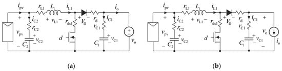
Figure 3.
PV boost-power-stage converter (a) at CO mode and (b) at VO mode.
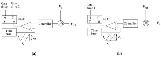
Figure 4.
Two different control-system arrangements: (a) conventional negative feedback arrangement; (b) inverted feedback arrangement.
The capacitor () of the PV generator (Figure 2) can be considered to be in parallel with the input capacitor of the converter, but it is not explicitly shown in the subsequent models. As Figure 2 shows, the value of the PV capacitance is very low at the CCR operating points of the generator, where it would not have effect on the converter behavior due to the input capacitor of the converter. It starts increasing in CVR, when all or a part of photocurrent flows through the internal diodes of the PV cells (i.e., its highest value takes palace in open-circuit condition), but the increase in the input terminal capacitance will have only insignificant effect on the converter behavior.
The dynamic analysis of the power stage will be performed assuming that the input source is a voltage source, when the MOSFET is controlled as in the conventional boost converter (i.e., the MOSFET conducts during the on-time), which is also the most common way of utilizing the boost-power-stage converter in PV applications [16]. In this case, the output-voltage-feedback-controlled converter is stable only in CVR. The dynamic analysis is also performed by inverting the MOSFET gate drive compared to the VF mode, and consequently, the input source is assumed to be a current source and the stable operation region CCR, respectively. Although the dynamic analysis may be performed without considering the input source specifically as voltage or current source as in [16,17,18], it is highly recommended to follow the procedures given in this paper for avoiding problems in control design and stability analysis. The dynamics of the conventional boost converter is well known [23,24], and therefore, it is covered only briefly. Comprehensive dynamic analysis of the current-fed boost-power-stage converter at current-output mode (Figure 3a) is presented in [21]. The corresponding voltage-output-mode (Figure 3b) transfer functions can be computed by means of the current-output-mode transfer functions by interchanging the input and output variables at the output terminal [25].
2.1. Small Signal Model of VF–VO Boost Converter
The set of transfer functions representing the dynamics of the boost-power-stage converter in Figure 3b, when the input source is considered to be an ideal voltage source (), can be given according to [24] as follows:
where and denote steady-state duty ratio and its complement, and the determinant (), , and are defined by
The corresponding operating point is given in Equation (3):
The RHP zero of the control-to-output-voltage transfer function () in Equation (1) (i.e., element (2,3)) can be given by
where . According to the behavior of the PV generator, the minimum value of within the CVR equals (i.e., ), if the input source is assumed to be an ideal voltage source. The input source is, however, not an ideal voltage source, but its internal impedance is considerable as discussed earlier. The effect of non-ideal source on the converter dynamics is treated in Section 2.3. As Equation (1) indicates, the input capacitor () affects only the input impedance of the converter due to the short-circuiting nature of the ideal voltage source. The contribution of the input capacitor including the PV-generator capacitor will be discussed in more detail when the source effect is treated in Section 2.3.
2.2. Small Signal Model of CF–VO Boost Converter
The set of transfer functions governing the dynamic behavior of the CF–VO boost converter in Figure 3b is given in Equation (5). The MOSFET gate-drive scheme is assumed to be such that the MOSFET is turned on during the off time (Figure 4a, Gate Drive 2). The set is derived from the set of transfer functions given in [21] by interchanging the input (i.e., ) and output (i.e., ) variables at the output terminal. The input source is assumed to be an ideal current source ().
where the determinant (), , , and are given in Equation (6), and and in Equation (7), respectively. The operating point of the converter is given in Equation (8), where the output voltage () is assumed to be constant, regulated by the output-voltage-feedback controller.
The numerator of the control-to-output-voltage transfer function (, the element (2,3)) in Equation (5)) indicates that the output-control dynamics contain two RHP zeros at approximately
where the first RHP zero resembles the zero, which is characteristic of CF converters [12], and the second RHP zero resembles the zero, which is characteristic of the VF boost converter, as given in Equation (4) [23]. The first zero is usually located at low frequencies, correspondingly limiting the crossover frequency of the feedback loop for ensuring stable operation. The PV generator as an input source is a highly nonlinear source, which would profoundly affect the dynamics of the PV-interfacing converter [8]. The PV-source effect on the CF converter dynamics is introduced in Section 2.3. In the case of a CF boost converter, the input capacitor affects the converter dynamics as a state variable (i.e., it will increase the system order by one), which is also visible in the denominator of the transfer functions in Equation (6). Equation (6) shows that the input-terminal capacitance (i.e., ) will affect the location of the resonance of the power stage.
2.3. Effect of PV Generator
It is well known that the PV generator is, in principle, a nonlinear current source [8]. Therefore, its equivalent circuit can be given as shown in Figure 5a, which is valid for all the operating points of the PV generator. However, if the interfacing converter is forced to operate as a voltage-fed converter (i.e., the MOSFET control scheme is as it is in the conventional VF converter, and the output-voltage feedback is activated) then the proper input source is a voltage-type source as shown in Figure 5b, because the input of the output-side feedback-controlled converter has the property of a current sink. A proper system also requires that the upstream and downstream sources within a certain interface have to be the duals of each other [24]. The output impedance of the PV generator (Figure 6) can be approximated by means of its dynamic resistance () and dynamic capacitance () [13] in the frequency range of interest (i.e., <10 kHz) in the interaction analyses as
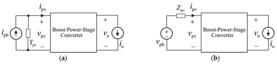
Figure 5.
PV-generator as an input source for (a) a CF converter and (b) a VF converter.
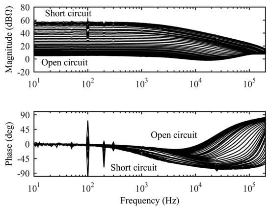
Figure 6.
Measured PV-generator output impedance of Raloss SR-30 PV panel, when the operating point is varied from open circuit to short circuit [12].
The sets of internal transfer functions of the VF and CF converters can in general be given as shown in Equation (11) (Equation (1)) and in Equation (12) (Equation (5)), where the superscript ‘VF’ denotes the voltage-fed transfer functions and the superscript ‘CF’ denotes the current-fed transfer functions, respectively. The physical meaning of the transfer functions of the matrices in Equations (11) and (12) can be easily concluded based on the corresponding input-variable (i.e., the right-most column vector) and output-variable (i.e., the left-most column vector) vectors. The names of the transfer functions may vary from author to author. The set of PV-generator-affected transfer functions for the VF converter can be found by replacing in Equation (11) with (Figure 5b), and for the CF converter can be found by replacing in Equation (12) with (Figure 5a):
where the sets of transfer functions (i.e., Equations (11) and (12)) correspond to the internal or unterminated transfer functions in Equations (1) and (5), respectively.
Following the above described procedures, the PV-generator-affected sets of transfer functions can be given by
where the transfer functions (i.e., the elements (1,1) and (2,1)), which are related to the input variables (Equation (13)) and (Equation (14)) cannot be measured in practice, because the input variables are not accessible.
For computing the PV-generator-affected control-to-output transfer functions () in Equations (13) and (14) (i.e., elements (2,3)), the ideal or infinite-bandwidth input admittance () and input impedance () are needed and they can be given by ([23,24] for more detailed explanations for the ideal admittances/impedances):
which indicate that when taking into account the inverting of the MOSFET gate signal in the CF converter compared to the VF converter. This outcome is quite expected, because the power stage and the output-terminal source are the same.
It is well known that the low-frequency output impedance () (Figure 6 and Equation (10)) will be responsible for the dynamic changes taken place in the converter as well as the stability of the PV-generator–converter interface [13]. Therefore, the PV-generator-affected control-to-output-voltage transfer functions can be computed according to Equations (13)–(15) (i.e., the elements (2,3) in Equations (13) and (14)) and the corresponding internal transfer functions in Equations (1) and (5) by replacing with and with , respectively. Following the described procedures, the PV-generator-affected control-to-output-voltage transfer function of the VF converter can be given by
and neglecting the parasitic elements by
Following the described procedures, the PV-generator-affected control-to-output-voltage transfer function of the CF converter can be given by
and neglecting the parasitic elements by
According to Equations (17) and (19), the PV-generator-affected control-to-output-voltage transfer functions are essentially the same except for the negative sign of the VF-converter in Equation (17). The analysis reveals that the low-frequency phase of Equation (17) starts at zero, when the converter is operated in CVR, because (Figure 1). The low-frequency phase will change by 180 degrees, when the converter enters into CCR. The analysis also reveals that the low-frequency phase of Equation (19) starts at zero, when the converter is operated in CCR, because (Figure 2). The low-frequency phase will change by 180 degrees, when the converter enters into CVR, respectively. This means that the conventional negative feedback arrangement (Figure 4a) can be applied for both of the converters in their proper operational regions, which will make the control design deterministic with no need for additional interpretations in terms of phase behavior.
The zeros in Equations (17) and (19) (i.e., the roots of ) can be approximated by
and
The simplified presentation of the zeros in Equations (20) and (21) as well as their locations in a complex plane can be justified as follows: It is known according to [21] that the zeros of Equations (17) and (19) are well separated. It is also known that the sum of the roots forms the coefficient of the first-order term and the product of the roots forms the zeroth-order term in a quadratic equation. If the zeroth-order term has a positive sign then the roots of the polynomial have the same sign. The negative sign of the first-order term then indicates that both of the roots lie in RHP. Such a condition takes place in CCR because . If both the zeroth-order and first-order terms have a negative sign then the roots have different signs and one of them is located in LHP and the other in RHP. Such a condition takes place in CVR because . Therefore, the zero in Equation (20) is located in RHP in CCR (i.e., ) and in LHP in CVR (i.e., ); the zero in Equation (21) is located in RHP all the time (i.e., ). At MPP (i.e., ), the zero in Equation (20) is located at the origin. The simplified locations of the zeros in Equations (20) and (21) would make the feedback-controller design convenient because the static resistance can always be computed by means of and . The controller design issues and the validity of the given simplified RHP-zero frequencies are discussed more in detail in Section 3.
The denominators of Equations (17) and (19) can be approximated as
when assuming that . in Equation (22) denotes either duty ratio (Equation (17)) or its complement (Equation (19)), but it naturally has the same numerical value because of denoting, in practice, the same operating point. The corresponding poles can be easily solved from Equation (22). The single zero in Equation (22) is located in CCR at a very low frequency and will actually prevent us from using a very simple integral (I) controller in the CF converter as well [12]. The undamped natural frequency () will be determined solely by the input capacitance () and the inductance (). In CVR (Figure 2), is small and so the damping factor () will not be small; therefore, the resonant behavior will be only moderate. The significant increase in the PV-generator capacitance () (Figure 1), when the operating point approaches the open-circuit condition, will decrease the damping factor and the undamped natural frequency only slightly.
2.4. Small-Signal Stability of PV-Generator–Converter Interface
In case of output-voltage-feedback control, the closed-loop input admittance (i.e., VF converter) and impedance (i.e., CF converter) of the interfacing converters can be given by
In the frequency range, where , (Note:), where the ideal impedances are given in Equation (15). According to Equation (15), can be given at the low frequencies by (Note: denotes ). When the feedback-system arrangement and the MOSFET control scheme are similar to the conventional VF boost converter (Figure 4a) [21] then the impedance-based stability analysis has to be performed similarly as instructed in [26] (i.e., the relevant minor-loop gain equals ). At the low frequencies, the impedance ratio becomes (Figure 5 and the above discussions on and ), and therefore the Nyquist stability criterion can be satisfied only when the converter operates in CVR (i.e., ) (Figure 2). If the converter enters into CCR (i.e., at MPP), the instability would take place by causing a collapse of the PV voltage and forcing a move into CCR, where the converter will be permanently unstable. The permanent instability is the consequence of the feedback system arrangement (Figure 4a), which tends to increase the duty ratio for increasing the corresponding output variables (i.e., output voltage), but in CCR the duty ratio shall be decreased [27] for increasing the output variables. Due to this conflict, the instability is permanent even if the overload condition has disappeared.
In the case of the CF converter, the relevant minor-loop gain is [12], and the converter would be stable only in CCR, where (Figure 2). The converter becomes unstable when entering into the CPR (i.e., at MPP). The instability will cause the PV voltage to collapse, and consequently the converter is forced back into the stable operational region (i.e., CCR). It should be noted that the on-time and off-time in a CF converter are interchanged compared to the VF converter, and therefore the voltage collapse automatically moves the CF converter into its stable region. If the cause of the instability is the permanent overload, then the converter naturally stays unstable. If the cause of instability is a transient-like overload, as discussed in [15], then the converter automatically recovers from instability when the overload condition has disappeared.
2.5. Discussion
The dynamic analyses presented in the previous subsections explicitly reveal that the analysis can be performed by substituting the PV generator with either its Norton (Section 2.2) or Thevenin (Section 2.1) equivalent circuit, as discussed in [28]. The choice of equivalent circuit cannot be done arbitrarily, however, because the feedback arrangement used and the active-switch control schemes would determine the equivalent circuit. If an improper equivalent circuit is used, for example, the stability assessment based on the impedance ratio of the PV-generator–converter interface will be incorrect, as clearly demonstrated in Section 2.4. In addition, the selection of equivalent circuit determines in which of the PV-generator regions the developed model is valid. The investigations also explicitly show (Equation (17) vs. Equation (1), element (2,3)) that the dynamic models of the conventional VF boost converter cannot be directly adopted for use in PV applications.
3. Boost-Power-Stage Converter Design
The experimental boost-power-stage converter is given in Figure 7 with the used power-stage components. Their selection is described more in detail in Section 3.1. The control system is built around Texas Instruments’ digital signal processor TMSF28335 (Texas Instruments Inc., Dallas, TX, USA). As discussed earlier, the future PV-interfacing converters are expected to be operated in grid-feeding (i.e., under input-voltage feedback control) and grid-forming (i.e., under output-voltage feedback control) modes. In Figure 7, the grid-feeding-mode circuit arrangement is denoted by red lines and the grid-forming mode by black lines. The input source of the converter has been the Raloss SR30-36 (Shanghai Raloss Energy Technology, Co., Ltd, Shanghai, China) PV module, which is composed of 36 series connected monocrystalline cells. The module is lighted by an artificial light source (Figure 8), which can produce irradiation of 500 W/m2, yielding a short-circuit current of 1.0 A, open-circuit voltage of 19.2 V, and MPP of 0.91 A @ 16 A at the module temperature of 45°. More information on the module can be found in [12].
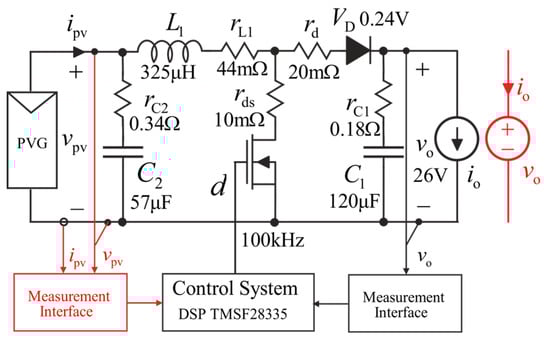
Figure 7.
Boost-power-stage converter with relevant component definitions.
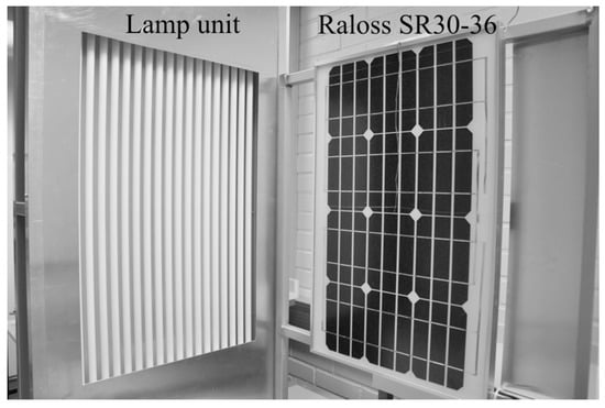
Figure 8.
Raloss SR30-36 PV panel and artificial light source.
Figure 9 shows the measured characteristics of the Raloss PV module in the environmental conditions of the experiments (Figure 9a: IV curve, Figure 9b: PV curve, and Figure 9c: and vs. ). Figure 10 shows expanded views of the behaviors of PV-module power (Figure 10a) as well as its dynamic and static resistances (Figure 10b) in the vicinity of the MPP (16 V). Figure 10a explicitly shows that the narrow region around the MPP exhibits constant power characteristics and hence it can be named as constant power region. Figure 10b also explicitly shows that the dynamic and static resistances are equal at the MPP but the dynamic resistance changes significantly when moving away from the MPP. The static resistance stays constant within CPR. Therefore, the changes in the converter dynamics will take place instantly when the operating point travels through the MPP. Figure 9 also shows that the CPR does not contribute any special features to the converter dynamics because does not stay constant and the equality between and is valid only at one specific point (i.e., at MPP), as the theory predicts [10]. The CPR only affects the MPP-tracking process due to the minimized PV power ripple [29,30]: The resolution and limited accuracy of the PV voltage and current measurements will prevent identifying the exact MPP within the CPR [29], which is also explicitly visible in Figure 10 (i.e., the PV power only changes by 0.3 W within the CPR).
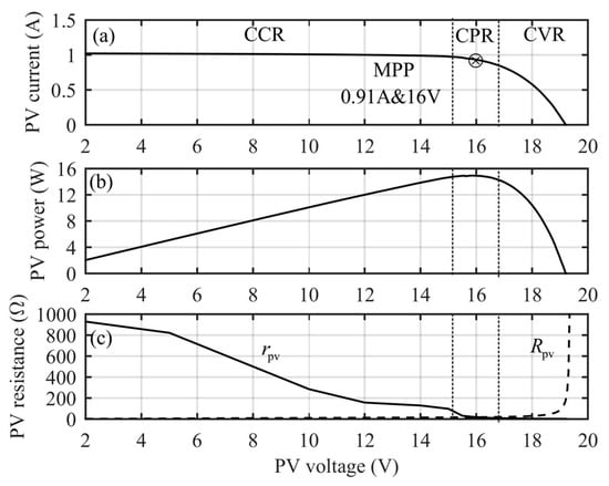
Figure 9.
Characteristics of Raloss SR30-36 PV module: (a) VI curve, (b) PV curve, and (c) and vs. .
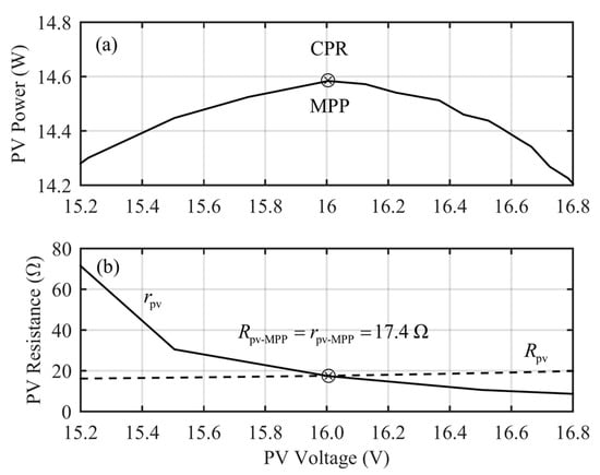
Figure 10.
Extended view of (a) and (b) and in the vicinity of MPP (i.e., in CPR).
3.1. Power Stage Component Selection
The value of the inductor was chosen in such a manner that its peak-to-peak current ripple equals 20% of the average inductor current. This procedure yields . The output capacitor was selected in such a manner that the undamped natural frequency () of the VF converter is less than (Equation (21)). The lowest frequency of the RHP zero in CVR equals approximately (i.e., ). In the case of lower irradiation conditions, the static resistance will increase due to the direct relation of irradiation and the short-circuit current of the PV generator [9], and thus the RHP zero will move to higher frequencies as well. In the given conditions, the RHP zero equals , and therefore . The value of was finally selected to be . The behavior of the CVR RHP zero is presented in Figure 11. The solid lines denote the frequency of the zero when it is computed based on according to Equation (21). The dashed lines denote the case where the zero is computed based on the first term in Equation (21). The dashed lines show that the simple and convenient estimate of the RHP-zero location would yield sufficiently accurate predictions without considering the effect of the dynamic resistance.
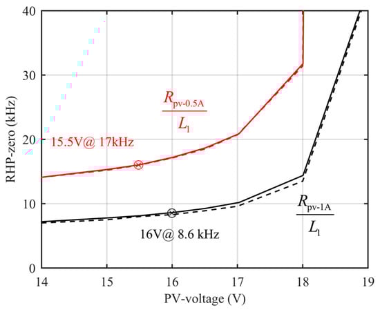
Figure 11.
The behavior of the CVR RHP zero when the operating point and the level of irradiation change. The solid lines denote the case where the location of the zero is computed based on , and the dashed lines, when the location is computed based on (Equation (21)). The black lines denote the short-circuit current of 1 A, and the red lines denote the short-circuit current of 0.5 A.
Selecting the value of the input-terminal capacitor () is quite complicated, because it affects both the location of the RHP zero in CCR (Equation (20)) as well as the location of the power-stage resonance in CVR, as shown in Equation (22). In CVR, the target for the output-voltage-feedback-loop crossover frequency is 2 kHz and in CCR it is as high as possible. The CVR target dictates that the resonant frequency should be half the crossover frequency or less. This places the lower limit for the input capacitance at .
Figure 12 shows the behavior of the CCR RHP zero (Equation (20)), when the operating point and the short-circuit current are varied and the input capacitance is assumed to be . The solid lines in Figure 12 denote the case where the CCR RHP zero is computed based on the more accurate term in Equation (20). The dashed lines denote the case where the CCR RHP zero is computed based on its simplified estimate as . The black lines denote the case where the short-circuit current is 1 A, and the red lines denote the case where the short-circuit current is 0.5 A, respectively. The analytical expression in Equation (20) indicates, and the solid lines in Figure 12 confirm, that the zero moves towards the origin when the operating point approaches the MPP. If assuming that the operating range has to be close to MPP (e.g., 15.5 V) and the input capacitance equals , then the corresponding zero locations are 350 Hz (at 1 A) and 110 Hz (at 0.5 A), respectively. In this specific case, the input capacitance was selected to be for ensuring proper operation in the vicinity of the MPP at the short-circuit current of 1 A. The corresponding RHP frequency is 480 Hz at 15.5 V. The selected input capacitance value yields the undamped natural frequency of the power stage as 1.2 kHz. If the frequency of the RHP zero is computed based on the simplified estimates (i.e., the dashed lines in Figure 12), then the RHP zero locations would be approximately three times higher than the realistic values.
Figure 12.
Behavior of RHP zero in CCR with respect to PV voltage and current.
3.2. Control Design in CVR
The measured (solid lines) and predicted (dots) PV-generator-affected control-to-output-voltage transfer functions are shown in Figure 13, where the blue curve lies already in CCR. The change of phase by 180 degrees clearly implies that instability would take place when the operating point travels through the MPP (16V) into CCR. The black and blue responses indicate that there exists only one RHP zero, as discussed in Section 2 (i.e., the slope of the magnitude changes from –40 dB to –20 dB at approximately 8 kHz). The target for the feedback-loop crossover frequency is 2 kHz.
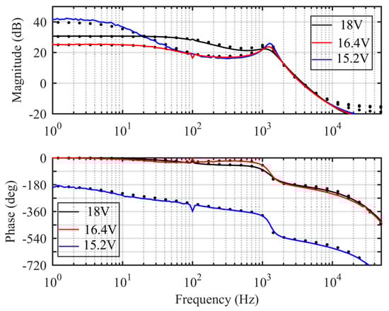
Figure 13.
The measured (solid lines) and predicted (dots) control-to-output-voltage transfer functions at PV voltages of 18V (black line), 16.4 V (red line), and 15.2 V (blue line).
According to the frequency responses of Figure 13 in CVR, the controller has to be a PID-type controller. The measurement interface in Figure 7 contains a low-pass filter, where the cut-off frequency is placed at half the switching frequency. As a consequence, the applicable controller is of the form
where , , and , respectively. The sampling and processing delay is approximated to be , where denotes the switching frequency. A second-order Padé approximation is used for approximating the effect of the delay on the feedback-loop behavior. The measured (solid lines) and predicted (dots) feedback loops are given in Figure 14 at PV voltages of 16.4 V and 18 V, respectively.
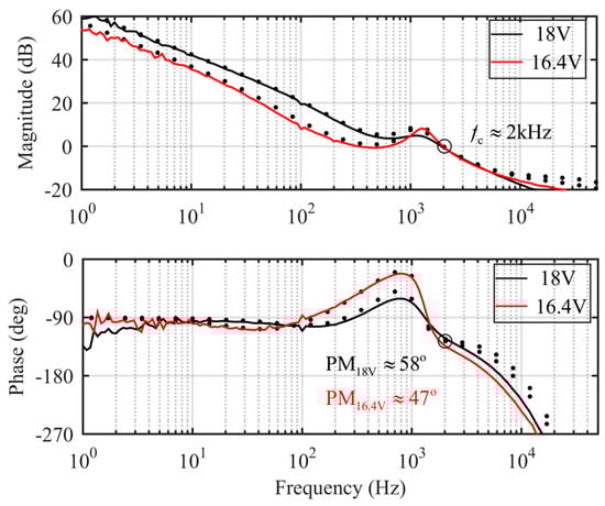
Figure 14.
The measured (solid lines) and predicted (dots) output-voltage feedback-loop gains at PV voltages of 18 V (black lines) and 16.4 V (red lines).
Figure 14 shows that the effect of the delay is very significant, and actually prevents us from obtaining a higher crossover frequency than 2 kHz with a sufficient phase margin. When the operating point approaches the MPP, the loop magnitude decreases down to unity in the frequency range from 300 Hz to 800 Hz, which naturally affects the behavior of the closed-loop output impedance, as shown in Figure 15 (red line). It is also well known [24] that the closed-loop output impedance would determine the load-transient behavior as well.
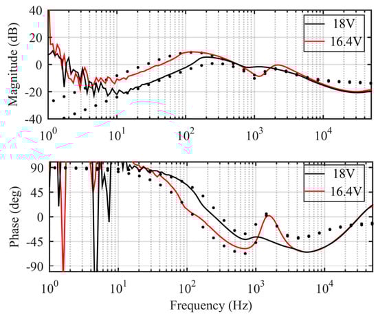
Figure 15.
The measured (solid lines) and predicted (dots) closed-loop output impedances at PV voltages of 18 V (black line) and 16.4 V (red line).
3.3. Control Design in CCR
The measured (solid lines) and predicted (dots) PV-generator-affected control-to-output-voltage transfer functions are shown in Figure 16, where the blue curve already lies in CVR. The change of phase by 180 degrees clearly implies that instability would result when the operating point travels through the MPP (16V) into CVR. The black and blue responses indicate that there are two RHP zeroes, as discussed in Section 2 (i.e., one at approximately 400 Hz and the other at 8 kHz (the red line)). The RHP zero locations can be identified by looking at the change of the slope of the loop magnitude (i.e., 400 Hz; from –20 dB/decade to 0 dB/decade, and 8 kHz, from –40 dB/decade to –20 dB/decade).
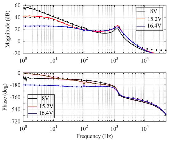
Figure 16.
The measured (solid lines) and predicted (dots) control-to-output-voltage transfer functions at PV voltages of 8V (black line), 15.2 V (red line), and 16.4 V (blue line).
The phase behavior (i.e., black and red lines) indicates that a PID controller has to be used, similarly to the case of the VF converter (Equation (24)), but the crossover frequency would be very low for robust stability to exist. The control design was carried out in such a manner that the crossover frequency was placed at 40 Hz, with the controller parameters as follows: , , and . In this case, the sampling and processing delay does not have any effect on the phase behavior. The measured (solid lines) and predicted (dots) output-voltage-feedback-loop responses are given in Figure 17. Similar to the case of the VF boost converter, the magnitude of the loop gain decreases when the operating point approaches the MPP, yielding a reduction in the crossover frequency to 15 Hz and an increase of the phase margin to 80 degrees. The low crossover frequency and rather high phase margin mean that the load transient response would be very sluggish, as discussed in [30].
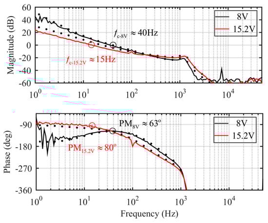
Figure 17.
The measured (solid lines) and predicted (dots) output-voltage loop gains at PV voltages of 8 V (black line) and 15.2 V (red line).
The measured (solid lines) and predicted (dots) closed-loop output impedance are given in Figure 18 at PV voltages of 8 V (black line) and 15.2 V (red line). As the figure shows, the output impedance is much higher than the closed-loop output impedance of the VF converter (Figure 15), implying an extremely poor transient response.
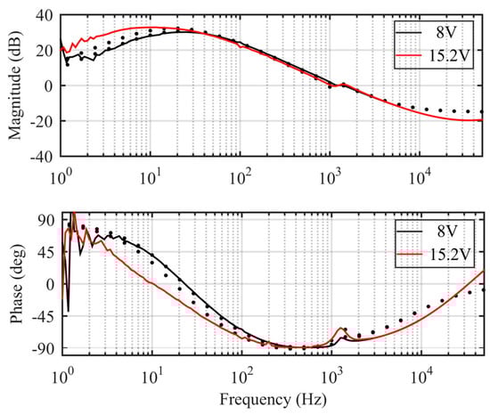
Figure 18.
The measured (solid lines) and predicted (dots) closed-loop output impedances at PV voltages of 8 V (black line) and 15.2 V (red line).
3.4. Discussion
In PV applications, the converter power stage and control designs are usually treated as if the input source were a rigid voltage source [31,32,33]. Viinamäki in [34] clearly show that the special features of the PV generator shall be considered carefully when selecting the power stage components and performing power loss analyses. The material provided in this paper also clearly shows that the PV-generator-fed VF-converter dynamic behavior differs significantly from the dynamic behavior of the conventional boost converter in terms of the number of RHP zeros, the order of the system as well as the resonance (the denominator in Equation (2) vs. the denominator in Equation (22)).
The control design issues presented in Section 3.2 and Section 3.3 clearly indicate that it is impossible, in practice, to design s control system for a CF converter providing robust stability without applying adaptive controller tuning [35,36] because of the knowledge on the behavior of PV-generator dynamic resistance that is required. In addition, its load-transient behavior would be inferior compared to the load-transient behavior of the VF boost converter. Hence, the application of the CF boost converter as a PV-generator-interfacing converter in grid-forming mode is not feasible.
It is commonly assumed that the size of the input capacitor of the DC–DC-interfacing converter shall be large enough to attenuate the grid-frequency-induced voltage ripple of the DC-link voltage to an acceptable level at the terminals of the PV generator, especially, in single-phase cascaded PV systems. Viinamäki in [37] show, however, that the voltage-ripple problem can be solved by applying proper output-voltage feedforward in a boost-power-stage converter. It was also clearly shown in this paper that the increase in the PV-generator capacitance does not pose real problems for the behavior of the interfacing converter.
4. Experimental Stability Assessment
As discussed earlier, the VF converter is bound to operate in a stable manner in CVR and the CF converter in CCR. Both of the converters will become unstable if the operating point travels through the MPP into the unstable region. Such a condition may take place, for example, as a consequence of the startup of AC loads or other transient phenomena in the AC grid, as discussed in [15]. It is also well known that the moving clouds would cause significant fluctuation in the power output of the PV generator, as shown in Figure 19, which would easily drive the operating point of the PV generator to an overload condition without additional energy storage that is properly controlled. The behavior of the VF and CF converters in such situations is treated in Section 4.1 and Section 4.2.
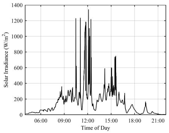
Figure 19.
Irradiation behavior due to clouds moving over the PV generator.
4.1. Voltage-Fed Boost Converter
Figure 20 shows the Nyquist plot of the measured impedance-based minor-loop gains (Section 2.4), when the operating point approaches the MPP. In vicinity of the MPP, the Nyquist plot will travel through the critical point (–1,0), indicating that the converter will be unstable in CCR, as discussed earlier. Figure 21 shows the time-domain behavior of the converter, when a step change of 0.4 A in the output current is applied at the time instant of and the converter enters into CCR. Figure 21 shows that the low-side MOSFET of the converter will stay permanently on due to the instability. Even if the load current is zero, the converter will not automatically recover from the instability. The converter can be recovered only by switching it off and performing a new startup in the open-circuit condition. Figure 20 also shows that the step of 0.4 A in the output current will only induce a dip of 0.3 V in the output voltage (Figure 21, in the vicinity of ), as the magnitude of the closed-loop output impedance would predict (Figure 15).
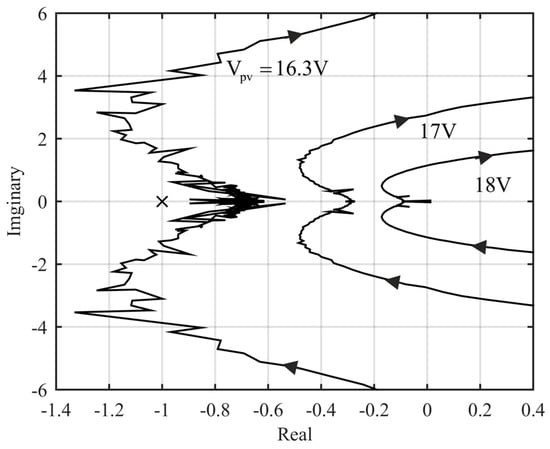
Figure 20.
The Nyquist plot of the impedance-based minor-loop gain, when the operating point moves towards the MPP.
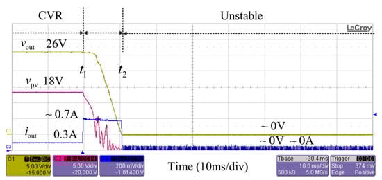
Figure 21.
The time-domain behavior of the converter when a step change in the output current is applied, shifting the operation point to the MPP and into CCR.
4.2. Current-Fed Boost Converter
Figure 22 shows the Nyquist plot of the measured impedance-based minor-loop gains (Section 2.4) at the PV-generator–converter interface, when the operating point approaches the MPP. In the vicinity of the MPP, the Nyquist plot will travel through the critical point (–1,0) indicating that the converter will be unstable in CVR. Figure 23 shows the time-domain behavior of the converter, when a step change in the output current is applied at and the converter enters into CVR. Figure 23 shows that the low-side MOSFET of the converter will stay permanently off due to the instability. When the load current is stepped back up to the original value at the time instant of , the converter starts up automatically. Figure 23 also shows that the step change of 0.18 A in the output current will induce a dip of 5 V in the output voltage (Figure 23, in vicinity of ), as the magnitude of the closed-loop output impedance would predict (Figure 18).
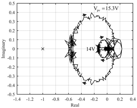
Figure 22.
The Nyquist plot of the impedance-based minor-loop gain when the operating point moves towards the MPP.
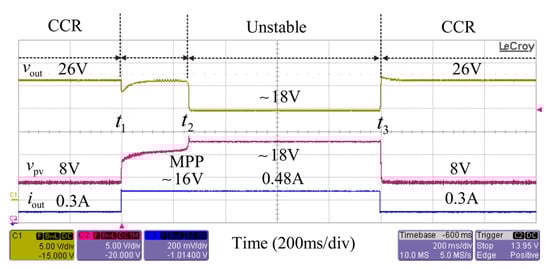
Figure 23.
The time-domain behavior of the converter when a step change in the output current is applied, shifting the operation point to the MPP and into CVR.
5. Conclusions
The main goal of this paper is to evaluate the dynamic behavior of the conventional boost-power-stage converter in future applications of the PV power systems, in which the interfacing converters have to be able to operate both in the grid-feeding and grid-forming modes. The grid-feeding-mode operation does not possess any such problems that would prevent the successful use of the conventional boost-power-stage converter in the named application. The investigations of this paper clearly show that the conventional boost-power-stage converter operates in a stable manner only in CVR, when the output-voltage feedback loop is closed as the grid-forming-mode operation requires. The dynamic behavior of the converter differs, however, from the dynamic behavior of the conventional boost converter, as explicitly shown in this paper. Its load-transient dynamics would also be acceptable due to the possibility of designing sufficiently high crossover frequency of the output-voltage feedback loop. The main limiting factor in the crossover frequency would be the sampling and processing delay due to digital control. When the operating point reaches the MPP, the converter becomes permanently unstable (i.e., the low-side MOSFET will stay permanently on). The only way to recover the converter into stable operation is to remove the feedback loop and start up the operation in open-loop mode.
The investigations of this paper clearly show that the CF mode of the boost-power-stage converter is not a feasible alternative to a PV-generator-interfacing converter in grid-forming-mode operation, because it cannot be designed to provide robust stability at all the desired operating points without the application of adaptive controller tuning techniques. In addition, its load transient dynamics would be inferior compared to the load transient dynamics of the VF boost converter, which may not be even acceptable for such an application.
The investigations presented in this paper also explicitly show that the stability analysis in the converter–generator interface can be performed assuming the PV generator either as a current or voltage source, when the duality between the upstream and downstream terminal sources within the interface is valid and the small-signal model of the converter corresponds to the chosen input terminal source. If these requirements are not valid, then the obtained stability information may not be valid either.
Acknowledgments
The work is funded by the Finnish Funding Agency for Innovation, TEKES, through the Finnish Solar Revolution research project.
Author Contributions
Jukka Viinamäki has been responsible for performing all the experimental parts related to the described research as well as writing the paper. Alon Kuperman and Teuvo Suntio have been involved in outlining the basic theories behind the research work as well as helping to write and evaluate the paper.
Conflicts of Interest
The authors declare no conflict of interest.
References
- Rocabert, J.; Luna, A.; Blaabjerg, F.; Rodríguez, P. Control of power converters in AC microgrids. IEEE Trans. Power Electron. 2012, 27, 4734–4749. [Google Scholar] [CrossRef]
- Diaz, N.L.; Coelho, E.A.; Vasquez, J.C.; Guerrero, J.M. Stability analysis for isolated AC microgrids based PV-active generators. In Proceedings of the IEEE Energy Convers. Congress & Expo (IEEE ECCE), Montreal, QC, Canada, 20–24 September 2015; pp. 4214–4221. [Google Scholar]
- Wang, J.; Chang, N.C.P.; Feng, X.; Monti, A. Design of a generalized control algorithm for parallel inverters for smooth microgrid transition operation. IEEE Trans. Ind. Electron. 2015, 62, 4900–4914. [Google Scholar] [CrossRef]
- Sangwongwanich, A.; Yang, Y.; Blaabjerg, F. High-performance constant power generation in grid-connected PV systems. IEEE Trans. Power Electron. 2016, 31, 1822–1825. [Google Scholar] [CrossRef]
- Yang, Y.; Wang, H.; Blaabjerg, F.; Kerekes, T. Hybrid power control concept for PV inverters with reduced thermal loading. IEEE Trans. Power Electron. 2014, 29, 6271–6275. [Google Scholar] [CrossRef]
- Tonkoski, R.; Lopes, L.; El-Fouly, T. Coordinated active power curtailment of grid connected PV inverters for overvoltage prevention. IEEE Trans. Sustain. Energy 2011, 2, 139–147. [Google Scholar] [CrossRef]
- Grainer, B.M.; Reed, G.F.; Sparacino, A.R.; Lewis, P.T. Power electronics for grid-scale energy storage. Proc. IEEE 2014, 102, 1000–1013. [Google Scholar] [CrossRef]
- Nousiainen, L.; Puukko, J.; Mäki, A.; Messo, T.; Huusari, J.; Jokipii, J.; Viinamäki, J.; Lobera, D.T.; Valkealahti, S.; Suntio, T. Photovoltaic generator as an input source for power electronic converters. IEEE Trans. Power Electron. 2013, 28, 3028–3038. [Google Scholar] [CrossRef]
- Liu, S.; Dougal, R.A. Dynamic multiphysics model for solar array. IEEE Trans. Energy Convers. 2002, 17, 285–294. [Google Scholar]
- Wyatt, J.L.; Chua, L.O. Nonlinear resistive maximum power theorem with solar cell application. IEEE Trans. Circuits. Syst. 1983, 30, 824–828. [Google Scholar] [CrossRef]
- Mäki, A.; Valkealahti, S.; Suntio, T. Dynamic terminal characteristics of a photovoltaic generator. In Proceedings of the 14th International Power Electronics and Motion Control Conference (EPE-PEMC), Ohric, Republic of Macedonia, 6–8 Septenber 2010. [Google Scholar]
- Suntio, T.; Leppäaho, J.; Huusari, J.; Nousiainen, L. Issues on solar-generator-interfacing with current-fed MPP-tracking converters. IEEE Trans. Power Electron. 2010, 25, 2409–2419. [Google Scholar] [CrossRef]
- Sitbon, M.; Leppäaho, J.; Suntio, T.; Kuperman, A. Dynamics of photovoltaic-generator-interfacing voltage-controlled buck power stage. IEEE J. Photovolt. 2015, 5, 633–640. [Google Scholar] [CrossRef]
- Leppäaho, J.; Suntio, T. Dynamic characteristics of current-fed superbuck converter. IEEE Trans. Power Electron. 2011, 26, 2409–2419. [Google Scholar] [CrossRef]
- Du, W.; Jiang, Q.; Erickson, M.J.; Lasseter, R.H. Voltage-source control of PV inverter in a CERTS microgrid. IEEE Trans. Power Del. 2014, 29, 1726–1734. [Google Scholar] [CrossRef]
- Konstantopoulos, G.C.; Alexandridis, T. Non-linear voltage regulator design for DC/DC boost converters used in photovoltaic applications: Analysis and experimental results. IET Renew. Power Gener. 2013, 7, 296–308. [Google Scholar] [CrossRef]
- Qin, L.; Xie, S.; Hu, M.; Yang, C. Stable operating area of photovoltaic cells feeding DC-DC converter in output voltage regulation mode. IET Renew. Power Gener. 2015, 9, 970–981. [Google Scholar] [CrossRef]
- Luo, S.; Qin, L.; Hu, M.; Hou, X.X.; Xie, S.J. Stable operating area of photovoltaic cells feeding the interface converter in output current regulation mode. In Proceedings of the IEEE 8th International Power Electron. Motion Control Conf. (IPEMC-ECCE Asia), Hefei, China, 22–26 May 2016; pp. 185–192. [Google Scholar]
- Golnas, A. PV system reliability: An operator’s perspective. IEEE J. Photovolt. 2013, 3, 416–421. [Google Scholar] [CrossRef]
- Petrone, G.; Spagnuolo, G.; Teodorescu, R.; Veerachary, M.; Vitelli, M. Reliability issues in photovoltaic power processing systems. IEEE Trans. Ind. Electron. 2008, 55, 2569–2580. [Google Scholar] [CrossRef]
- Viinamäki, J.; Jokipii, J.; Messo, T.; Suntio, T.; Sitbon, M.; Kuperman, A. Comprehensive dynamic analysis of PV-generator-interfacing DC-DC boost-power-stage converter. IET Renew. Power Gener. 2015, 9, 306–314. [Google Scholar] [CrossRef]
- Wen, B.; Boroyevich, D.; Burgos, R.; Mattavelli, P.; Shen, Z. Inverse Nyquist stability criterion for grid-tied inverters. IEEE Trans. Power Electron. 2017, 32, 1548–1556. [Google Scholar] [CrossRef]
- Erickson, R.W.; Maksimović, D. Fundamentals of Power Electronics, 2nd ed.; Kluwer Academic Publishers: Norwell, MA, USA, 2001. [Google Scholar]
- Suntio, T. Dynamic Profile of Switched-Mode Converter—Modeling, Analysis and Control; Wiley-VCH: Weinheim, Germany, 2009. [Google Scholar]
- Suntio, T.; Huusari, J.; Leppäaho, J. Issues on solar-generator interfacing with voltage-fed MPP-tracking converters. Eur. Power Electron. Drives. J. 2010, 20, 40–47. [Google Scholar] [CrossRef]
- Middlebrook, R.D. Design techniques for preventing input-filter oscillations in switched-mode regulators. In Proceedings of the 5th National Solid State Power Conversion Conference (POWERCON 5), San Francisco, CA, USA, 4–6 May 1978; pp. A3.1–A3.16. [Google Scholar]
- Xiao, W.; Dunford, W.G.; Palmer, P.R.; Capel, A. Regulation of photovoltaic voltage. IEEE Trans. Ind. Electron. 2007, 54, 1365–1374. [Google Scholar] [CrossRef]
- Chen, Y.-M.; Huang, A.Q.; Yu, X. A high step-up three-port DC-DC converter for standalone PV/battery power systems. IEEE Trans. Power Electron. 2013, 28, 5049–5062. [Google Scholar] [CrossRef]
- Kivimäki, J.; Sitbon, M.; Kolesnik, S.; Kuperman, A.; Suntio, T. Sampling frequency design to optimize MPP tracking performance for open-loop operated converters. In Proceedings of the 42nd Annual Conference of the IEEE Industrial Electronics Society, Florence, Italy, 23–26 October 2016; pp. 3093–3098. [Google Scholar]
- Kivimäki, J.; Kolesnik, S.; Sitbon, M.; Suntio, T.; Kuperman, A. Design guidelines for multi-loop perturbative maximum power point tracking algorithms. IEEE Trans. Power Electron. 2017, in press. [Google Scholar]
- Ho, C.N.M.; Breuninger, H.; Pettersson, S.; Escobar, G.; Serpa, L.A.; Coccia, A. Practical design and implementation procedure of an interleaved boost converter using SiC diodes for PV applications. IEEE Trans. Power Electron. 2012, 27, 2835–2845. [Google Scholar] [CrossRef]
- Adinolfi, G.; Graditi, G.; Siano, P.; Piccolo, A. Multiobjective optimal design of photovoltaic synchronous boost converters assessing efficiency, reliability, and cost savings. IEEE Trans. Ind. Inform. 2015, 11, 1038–1048. [Google Scholar] [CrossRef]
- Fard, M.; Aldeen, M. Robust control design for a boost converter in a photovoltaic system. In Proceedings of the 7th International Symposium Power Electronics for Distributed Generation Systems (IEEE PEDG), Vancouver, BC, Canada, 27–30 June 2016; pp. 1–9. [Google Scholar]
- Viinamäki, J.; Kivimäki, J.; Suntio, T.; Hietalahti, L. Design of boost-power-stage converter for PV generator interfacing. In Proceedings of the 16th European Conference on Power Electronics and Applications (EPE ECCE Europe), Lappeenranta, Finland, 26–28 August 2014; pp. 1–10. [Google Scholar]
- Sitbon, M.; Schacham, S.; Suntio, T.; Kuperman, A. Improved adaptive input voltage control of a solar array interfacing current mode controlled boost power stage. Energy Convers. Manag. 2015, 98, 369–375. [Google Scholar] [CrossRef]
- Urtasun, A.; Sanchis, P.; Marroyo, L. Adaptive voltage control of the DC/DC boost stage in PV converters with small input capacitor. IEEE Trans. Power Electron. 2013, 28, 5038–5048. [Google Scholar] [CrossRef]
- Viinamäki, J.; Jokipii, J.; Suntio, T. Improving double-line-frequency ripple rejection capability of DC/DC converter in grid connected two stage PV inverter using DC-link voltage feedforward. In Proceedings of the 18th European Conference on Power Electronics and Applications (EPE-ECCE Europe), Karlsruhe, Germany, 5–9 September 2016; pp. 1–10. [Google Scholar]
© 2017 by the authors. Licensee MDPI, Basel, Switzerland. This article is an open access article distributed under the terms and conditions of the Creative Commons Attribution (CC BY) license (http://creativecommons.org/licenses/by/4.0/).