Extremely Efficient Design of Organic Thin Film Solar Cells via Learning-Based Optimization


Abstract
:1. Introduction
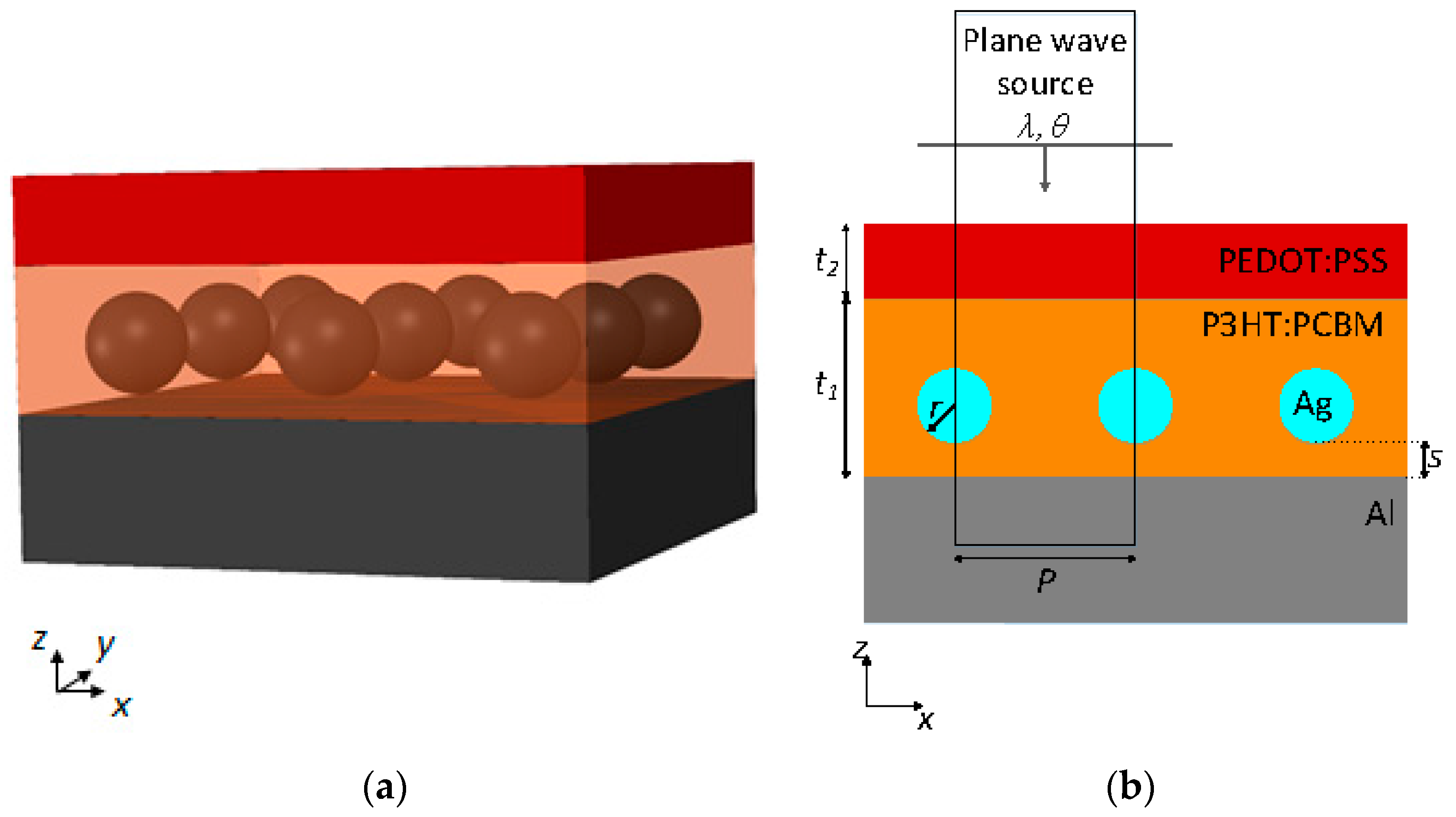
2. Description of the Physical Model
3. Surrogate-Based Modeling and Optimization
3.1. Neural Network Model of Absorptivity
3.2. Objective Function
3.3. Optimization Algorithms
4. Results and Discussion
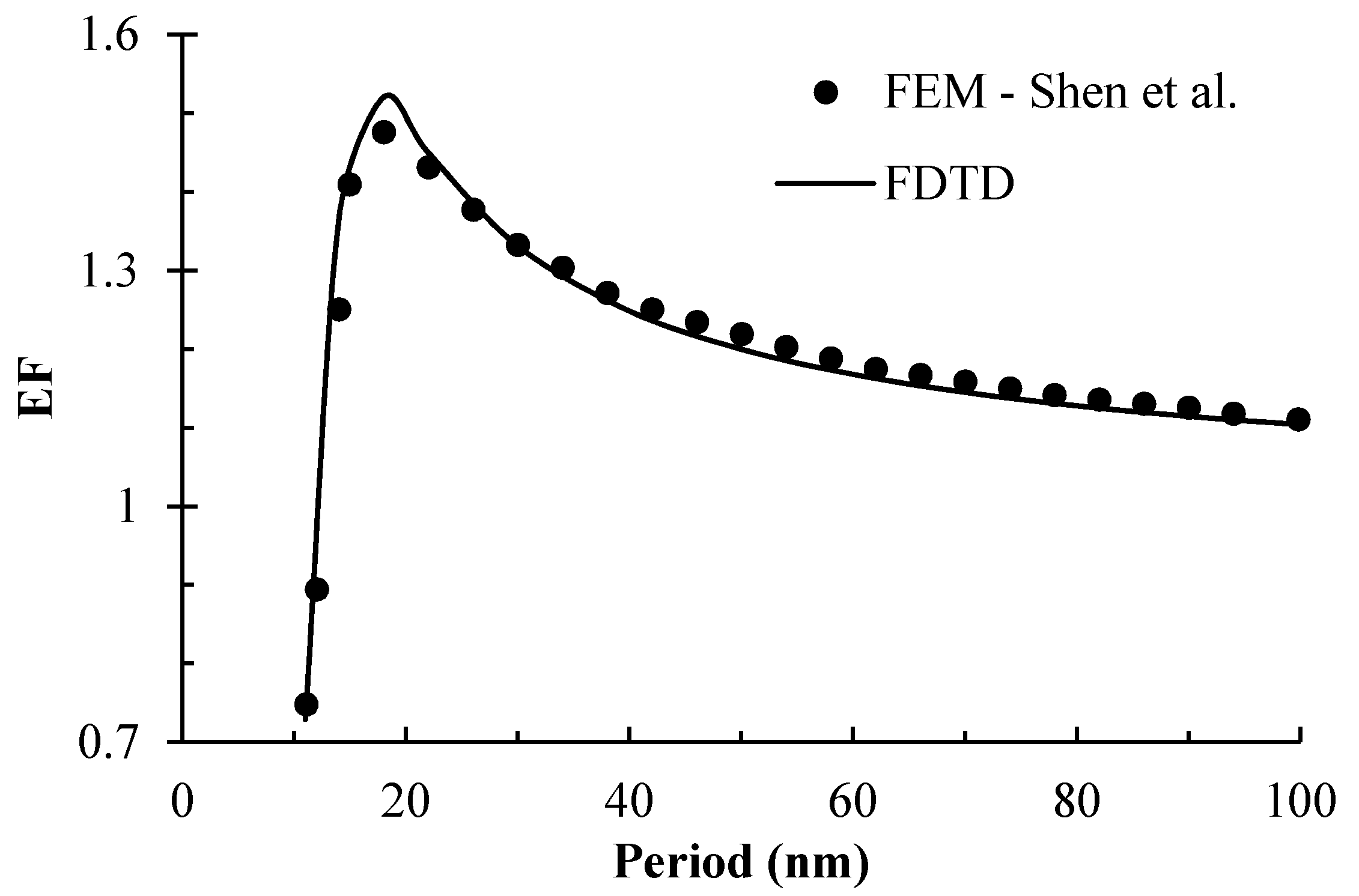
4.1. Data Generation
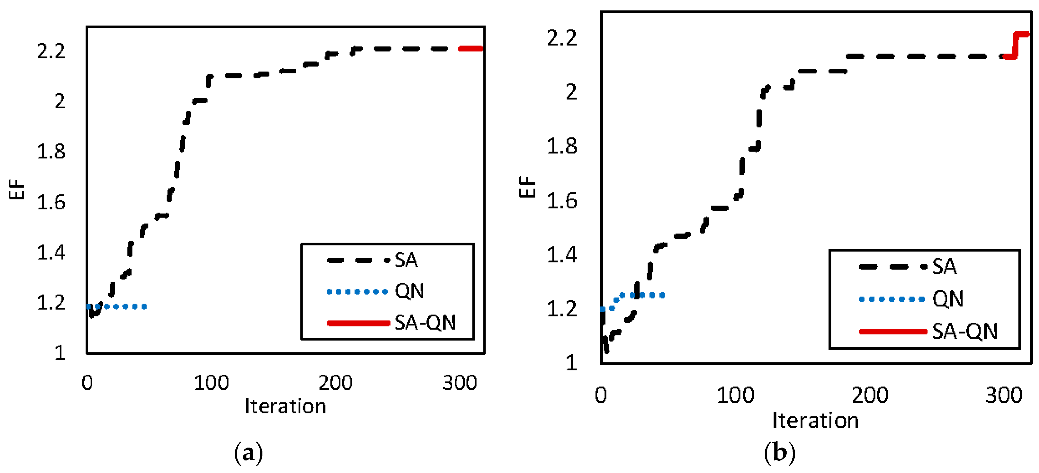
4.2. Results of Optimization
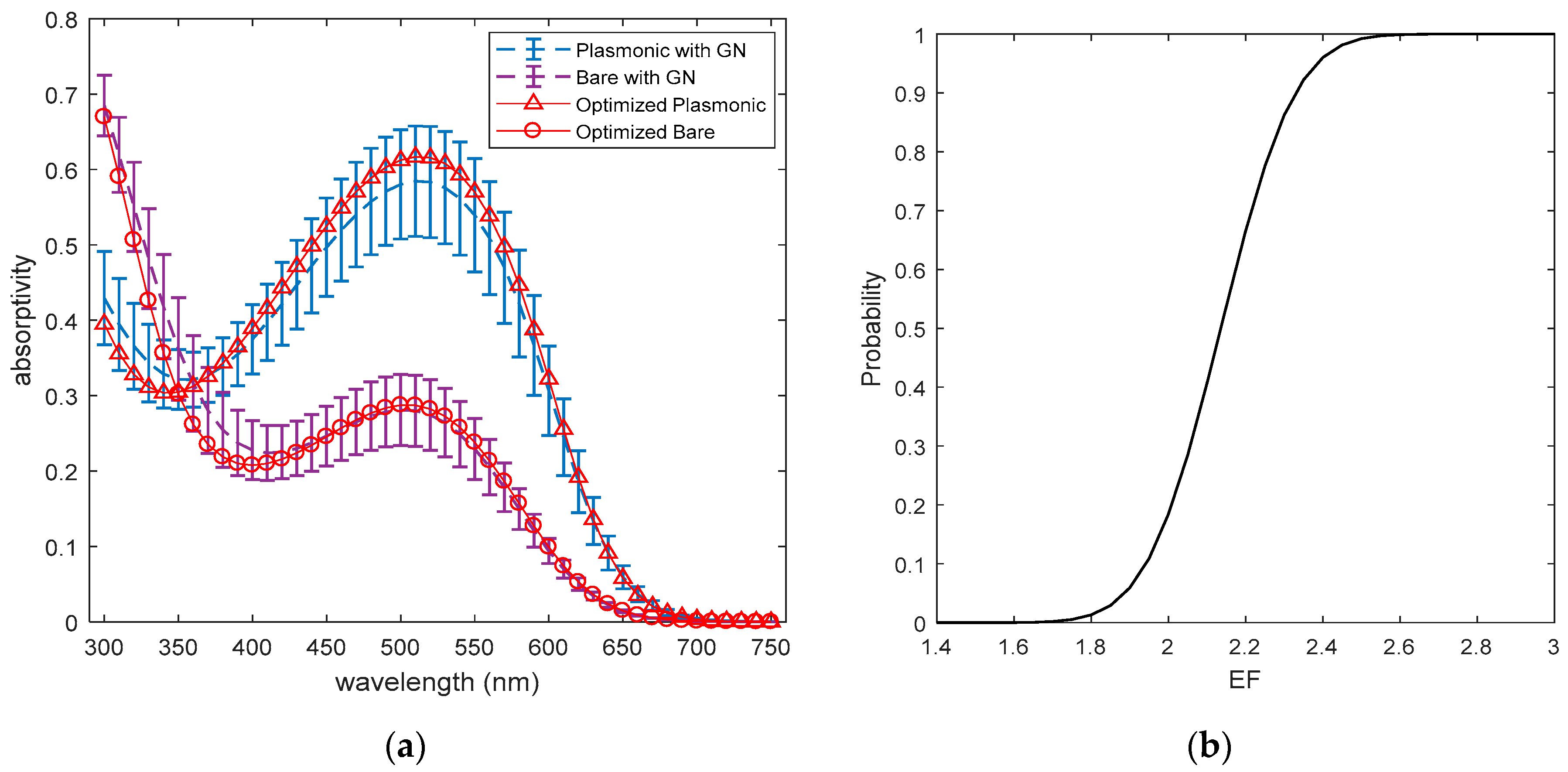
4.3. Uncertainty Analysis
5. Conclusions
Author Contributions
Conflicts of Interest
Nomenclature
| cost function | |
| Error vector | |
| Enhancement factor | |
| solar spectrum | |
| number of layers | |
| Ag radius | |
| vertical distance of Ag from bottom | |
| Marquardt sensitivity | |
| P3HT:PCBM thickness | |
| PEDOT:PSS thickness | |
| coefficient matrix | |
| geometry vector | |
| Coefficient vector | |
| normalized NN input and outputs |
Greek Letters
| regularization parameter | |
| Wavelength | |
| Lagrange multipliers | |
| incidence angle |
Subscripts
| Bare | |
| Plasmonic |
Superscripts
| Iteration | |
| Lower/upper limit |
Appendix A. Explicit Computation of Gradient in Neural Networks for QN Optimization
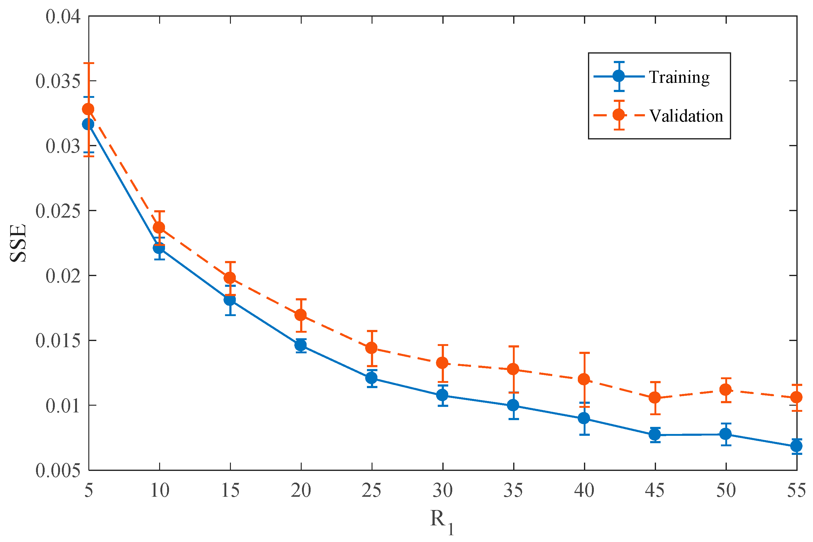
Appendix B. Neural Network Training and Validation

References
- National Renewable Energy Laboratory Renewable Electricity Generation and Storage Technologies Futures Study. Available online: https://www.nrel.gov/docs/fy12osti/52409-2.pdf (accessed on 25 October 2017).
- Fu, R.; Chung, D.; Lowder, T.; Feldman, D.; Ardani, K.; Fu, R.; Chung, D.; Lowder, T.; Feldman, D.; Ardani, K. U.S. Solar Photovoltaic System Cost Benchmark: Q1 2016. Available online: https://www.nrel.gov/docs/fy16osti/66532.pdf (accessed on 20 October 2017).
- Sai, H.; Kanamori, Y.; Arafune, K.; Ohshita, Y.; Yamaguchi, M. Light Trapping Effect of Submicron Surface Textures in Crystalline Si Solar Cells. Prog. Photovolt. Res. Appl. 2007, 15, 415–423. [Google Scholar] [CrossRef]
- Ferry, V.E.; Verschuuren, M.A.; Li, H.B.; Verhagen, E.; Walters, R.J.; Schropp, R.E.; Atwater, H.A.; Polman, A. Light trapping in ultrathin plasmonic solar cells. Opt. Express 2010, 18, A237–A245. [Google Scholar] [CrossRef] [PubMed]
- Catchpole, K.R.; Polman, A. Plasmonic solar cells. Opt. Express 2008, 16, 21793–21800. [Google Scholar] [CrossRef] [PubMed]
- Atwater, H.A.; Polman, A. Plasmonics for improved photovoltaic devices. Nat. Mater. 2010, 9, 205–213. [Google Scholar] [CrossRef]
- Hajimirza, S.; El Hitti, G.; Heltzel, A.; Howell, J. Using inverse analysis to find optimum nano-scale radiative surface patterns to enhance solar cell performance. Int. J. Therm. Sci. 2012, 62, 93–102. [Google Scholar] [CrossRef]
- Hajimirza, S. Expedited Quasi-Updated Gradient Based Optimization Techniques for Energy Conversion Nano-Materials. J. Nanoelectron. Optoelectron. 2015, 10, 140–146. [Google Scholar] [CrossRef]
- Hajimirza, S.; Howell, J.R. Flexible Nanotexture Structures for Thin Film PV Cells Using Wavelet Functions. IEEE Trans. Nanotechnol. 2015, 14, 904–910. [Google Scholar] [CrossRef]
- Hajimirza, S. A novel machine-learning aided optimization technique for material design: Application in thin film solar cells. In Proceedings of the ASME 2016 HT/FEDSM/ICNMM Summer Heat Transfer Conference, Washington, DC, USA, 10–14 July 2016. [Google Scholar]
- Hajimirza, S.; Howell, J.R. Design and analysis of spectrally selective patterned thin-film cells. Int. J. Thermophys. 2013, 34, 1930–1952. [Google Scholar] [CrossRef]
- Hajimirza, S.; Howell, J.R. Statistical Analysis of Surface Nanopatterned Thin Film Solar Cells Obtained by Inverse Optimization. J. Heat Transf. 2013, 135, 91501. [Google Scholar] [CrossRef]
- Das, N.; Islam, S. Design and analysis of nano-structured gratings for conversion efficiency improvement in GaAs solar cells. Energies 2016, 9, 690. [Google Scholar] [CrossRef]
- Nguyen, A.T.; Reiter, S.; Rigo, P. A review on simulation-based optimization methods applied to building performance analysis. Appl. Energy 2014, 113, 1043–1058. [Google Scholar] [CrossRef]
- Yan, S.; Minsker, B. Optimal groundwater remediation design using an Adaptive Neural Network Genetic Algorithm. Water Resour. Res. 2006, 42, 1–14. [Google Scholar] [CrossRef]
- Salah, C.B.; Ouali, M. Comparison of fuzzy logic and neural network in maximum power point tracker for PV systems. Electr. Power Syst. Res. 2011, 81, 43–50. [Google Scholar] [CrossRef]
- Heidari, E.; Sobati, M.A.; Movahedirad, S. Accurate prediction of nanofluid viscosity using a multilayer perceptron artificial neural network (MLP-ANN). Chemom. Intell. Lab. Syst. 2016, 155, 73–85. [Google Scholar] [CrossRef]
- Krebs, F.C. Fabrication and processing of polymer solar cells: A review of printing and coating techniques. Sol. Energy Mater. Sol. Cells 2009, 93, 394–412. [Google Scholar] [CrossRef]
- Ameri, T.; Dennler, G.; Lungenschmied, C.; Brabec, C.J. Organic tandem solar cells: A review. Energy Environ. Sci. 2009, 2, 347–363. [Google Scholar] [CrossRef]
- Gunes, S.; Neugebauer, H.; Sariciftci, N.S. Conjugated Polymer-Based Organic Solar Cells. Chem. Rev. 2007, 107, 1324–1338. [Google Scholar] [CrossRef] [PubMed]
- Scharber, M.C. On the Efficiency Limit of Conjugated Polymer: Fullerene-Based Bulk Heterojunction Solar Cells. Adv. Mater. 2016, 28, 1994–2001. [Google Scholar] [CrossRef] [PubMed]
- Min, J.; Bronnbauer, C.; Zhang, Z.G.; Cui, C.; Luponosov, Y.N.; Ata, I.; Schweizer, P.; Przybilla, T.; Guo, F.; Ameri, T.; et al. Fully Solution-Processed Small Molecule Semitransparent Solar Cells: Optimization of Transparent Cathode Architecture and Four Absorbing Layers. Adv. Funct. Mater. 2016, 26, 4543–4550. [Google Scholar] [CrossRef]
- Zhao, W.; Li, S.; Yao, H.; Zhang, S.; Zhang, Y.; Yang, B.; Hou, J. Molecular Optimization Enables over 13% Efficiency in Organic Solar Cells. J. Am. Chem. Soc. 2017, 139, 7148–7151. [Google Scholar] [CrossRef] [PubMed]
- Sciuto, G.L.; Capizzi, G.; Salvatore, C.O.C.O.; Shikler, R. Geometric shape optimization of organic solar cells for efficiency enhancement by neural networks. In Advances on Mechanics, Design Engineering and Manufacturing; Springer: Berlin, Germany, 2017; pp. 789–796. [Google Scholar]
- Zhao, D.W.; Tan, S.T.; Ke, L.; Liu, P.; Kyaw, A.K.K.; Sun, X.W.; Lo, G.Q.; Kwong, D.L. Optimization of an inverted organic solar cell. Sol. Energy Mater. Sol. Cells 2010, 94, 984–991. [Google Scholar] [CrossRef]
- Zayats, A.V.; Smolyaninov, I.I.; Maradudin, A.A. Nano-optics of surface plasmon polaritons. Phys. Rep. 2005, 408, 131–314. [Google Scholar] [CrossRef]
- Moreno, F.; García-Cámara, B.; Saiz, J.M.; González, F. Interaction of nanoparticles with substrates: Effects on the dipolar behaviour of the particles. Opt. Express 2008, 16, 12487–12504. [Google Scholar] [CrossRef] [PubMed]
- Palik, E.D. Handbook of Optical Constants of Solids; Academic press: New York, NY, USA, 1998; Volume 3. [Google Scholar]
- Rand, B.P.; Peumans, P.; Forrest, S.R. Long-range absorption enhancement in organic tandem thin-film solar cells containing silver nanoclusters. J. Appl. Phys. 2004, 96, 7519–7526. [Google Scholar] [CrossRef]
- Shen, H.; Bienstman, P.; Maes, B. Plasmonic absorption enhancement in organic solar cells with thin active layers. J. Appl. Phys. 2009, 106, 073109. [Google Scholar] [CrossRef]
- American Society for Testing and Materials. ASTM Standard Tables for Reference Solar Spectral Irradiances. 2003. Available online: http:www.astm.org (accessed on 20 September 2017).
- Lumerical Inc. Available online: https://www.lumerical.com/ (accessed on 15 June 2017).
- Queipo, N.V.; Haftka, R.T.; Shyy, W.; Goel, T.; Vaidyanathan, R.; Tucker, P.K. Surrogate-based analysis and optimization. Prog. Aerosp. Sci. 2005, 41, 1–28. [Google Scholar] [CrossRef]
- Hagan, M. T.; Demuth, H. B.; Beale, M. H.; De Jesus, O. Neural Network Design; PWS Publishing Company: Boston, MA, USA, 2014; ISBN 9780971732117. [Google Scholar]
- Foresee, F.D.; Hagan, M.T. Gauss-Newton approximation to Bayesian regularization. In Proceedings of the 1997 International Joint Conference on Neural Networks, Houston, TX, USA, 9–12 June 1997; pp. 1930–1935. [Google Scholar]
- Fletcher, R. Practical Methods of Optimization, 2nd ed.; John Wiley and Sons: New York, NY, USA, 2000. [Google Scholar]
- Cavazzuti, M. Optimization Methods: From Theory to Design; Springer Science & Business Media: Berlin, Germany, 2013. [Google Scholar]
- Karaboga, D.; Basturk, B. A powerful and efficient algorithm for numerical function optimization: Artificial bee colony (ABC) algorithm. J. Glob. Optim. 2007, 39, 459–471. [Google Scholar] [CrossRef]
- Deb, K.; Pratap, A.; Agarwal, S.; Meyarivan, T. A fast and elitist multiobjective genetic algorithm: NSGA-II. IEEE Trans. Evol. Comput. 2002, 6, 182–197. [Google Scholar] [CrossRef]
- Glover, F. Tabu search—Part I. ORSA J. Comput. 1989, 1, 190–206. [Google Scholar] [CrossRef]
- Kirkpatrick, S.; Gelatt, C.D.; Vecchi, M.P. Optimization by Simulated Annealing. Science 1983, 220, 671–680. [Google Scholar] [CrossRef] [PubMed]
- Ingber, L. Very fast simulated re-annealing. Math. Comput. Model. 1989, 12, 967–973. [Google Scholar] [CrossRef]


| Input Name | |||||||
|---|---|---|---|---|---|---|---|
| Lower Bound | 10 | 5 | 0 | 2 | 5 | 0 | 300 |
| Upper Bound | 100 | 200 | 100 | 89 | 900 |
| Method | EF | ||
|---|---|---|---|
| NN–QN | 1.26 | ||
| NN–SA | 2.21 | ||
| NN–SA–QN | 2.21 | ||
| NN–QN | 1.25 | ||
| NN–SA | 2.14 | ||
| NN–SA–QN | 2.22 |
© 2017 by the authors. Licensee MDPI, Basel, Switzerland. This article is an open access article distributed under the terms and conditions of the Creative Commons Attribution (CC BY) license (http://creativecommons.org/licenses/by/4.0/).
Share and Cite
Kaya, M.; Hajimirza, S. Extremely Efficient Design of Organic Thin Film Solar Cells via Learning-Based Optimization. Energies 2017, 10, 1981. https://doi.org/10.3390/en10121981
Kaya M, Hajimirza S. Extremely Efficient Design of Organic Thin Film Solar Cells via Learning-Based Optimization. Energies. 2017; 10(12):1981. https://doi.org/10.3390/en10121981
Chicago/Turabian StyleKaya, Mine, and Shima Hajimirza. 2017. "Extremely Efficient Design of Organic Thin Film Solar Cells via Learning-Based Optimization" Energies 10, no. 12: 1981. https://doi.org/10.3390/en10121981
APA StyleKaya, M., & Hajimirza, S. (2017). Extremely Efficient Design of Organic Thin Film Solar Cells via Learning-Based Optimization. Energies, 10(12), 1981. https://doi.org/10.3390/en10121981