1. Introduction
Due to their ability to automatically produce clear images of an object plane that has extremely varying illumination levels, wide dynamic range image sensors are required for many applications such as cameras for security systems, automobiles and industry. There have been various approaches to enhance the dynamic range of CMOS image sensors [
1-
6]. However, the non-linear response type wide dynamic range CMOS image sensor are not preferable for color images [
1,
2], while the linear response type such as CMOS image sensor with in-pixel lateral overflow integration capacitor is not appropriate for small pixels due to their complex pixel structure [
3]. The multiple exposures technique is one of the solutions for dynamic range enhancement. However the conventional technique of multiple exposures has a problem with the motion artifact due to signal loss during integration [
4-
6]. One of the most recent techniques to enhance the dynamic range of CMOS image sensors is the partial charge transfer technique [
7,
8]. It provides a signal at short accumulation in addition to a signal at long accumulation by continuing charge accumulation. In this technique, there is no degradation of the sensitivity in the wide dynamic range operation [
7]. The difference of two charge accumulation time in one frame period expands the dynamic range of the sensor. This technique uses a normal four transistors active pixel sensor (4T-APS) with an adjustable midpoint drive for the transfer gate. By using two types of accumulation time and two different drives to control the transfer gate during accumulation and readout, two set of output signals can be obtained from a single photodiode. The wide dynamic range signal can be synthesized from the two types of signals mentioned. Although it enhances the dynamic range of the sensor, the partial charge transfer technique also contributes to less sensitivity loss as compared to the conventional dynamic range expansion technique because it makes efficient use of full exposure by continuation of charge integration and maximize the fill factor. However, the short accumulation signal obtained from partial transfer operation is non-linear with respect to the incident light [
9]. In this paper, an analysis of the nonlinearity due to the partial charge transfer in the synthesized signals has been carried, and the relationship between the dynamic range and the non-linearity is deliberated by discussing out the pixel structure, the dynamic range expansion by partial charge transfer, the principle of charge transfer, the non-linearity due to current diffusion and the non-linearity due to initial condition of photodiode.
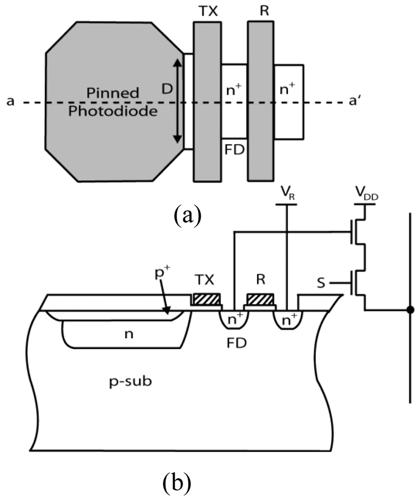
2. Pixel Structure
The simplified layout of the pixel and its cross-section at line aa' are shown in
Figures 1a,b, respectively. The pixel is a normal 4T-APS. However, the supply voltage for the transfer gate driver is designed to be adjustable for partial and whole charge transfer. To achieve high performance, the photodiode in the pixel has to be optimized. The shape of photodiode layout, the structure of photodiode, and the layout have significant influences on the performance of the whole imager [
10,
11]. In the pixel, the photodiode (PD) is designed with an octagonal shape with a small width,
D that is placed on the PD side for the purpose of improving the imager's performance. The use of buried PD is aimed to reduce the dark current of the pixel. However, the n layer near the transfer gate is not totally covered by p
+ layer and still contributes to the dark current. Therefore, by using a small
D, the dark current can be reduced because the area of uncovered n layer is decreased.
The use of octagonal shape for PD can increase the speed of charge flow during charge transfer operation, preventing image lag [
12]. In rectangular PD, the accumulated charge remains at the corners of PD during charge transfer operation resulting in a slower charge transfer. Moreover, the octagonal shape of photodiode dedicated to 12% lower interconnection surface and has a better spectral response compared to the rectangular photodiode [
13]. Besides, using the normal 4T-APS can be an advantage for this technique because high field factor can easily be obtained.
Table 1 shows the characteristics of the simulated pixel.
3. Dynamic Range Expansion by Partial Charge Transfer
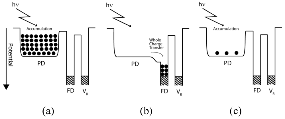
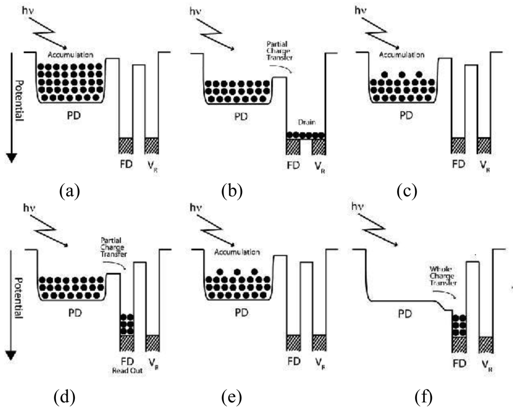
The principle of the dynamic range expansion by the partial charge transfer technique is discussed in this section. In this sensor, one frame of accumulation time is divided into two sub-frames.
The next steps explain the operation of the wide dynamic range image sensor with partial transfer:
When a strong light is irradiated on the pixel, the accumulated charge in the PD reaches the saturation level (Qmax) in short time. Since the signal is saturated, it cannot be read out at this time, therefore, the accumulated charge is partially drained and charge accumulation is repeated. The newly accumulated charge is partially transferred and read out. As a result, a short accumulation time signal is obtained.
In the final sub-frame, the accumulated charge is partially drained and charge accumulation is repeated.
Finally, a whole charge transfer operation is done and the transferred signal to the floating diffusion (FD) is read out.
From the operation, two set of output signals is obtained from a single photodiode, the long and short accumulation time signals. A Wide dynamic range image can be synthesized from the two setS of acquired signals because the difference of charge accumulation time can sufficiently expand the dynamic range of the sensor.
The signal from wholly transferred charge in the final sub-frame determines which signals have to be used, whether the long accumulation or the partially transferred short accumulation time signals. A method to judge which signals to be used is proposed. If the quantity of accumulated charge reaches a threshold value, QT at the end of final sub-frame and it is read out, the short accumulation signal is selected, if it is less than QT, the long accumulation time signal is used. The most important task in operating this sensor is identifying the value of QT.
In the case of a weak light irradiated on the pixel, the same operation (1)∼(3) is performed. However, the read data at the end of first sub-frame is 0 because the accumulated charge in photodiode does not exceed threshold level, QT. In the final sub-frame, the accumulated charge also does not exceed QT. Therefore, only the long accumulation signal is used in synthesized wide dynamic range image prior to the output signal in final sub-frame does not exceed the s threshold value, QT.
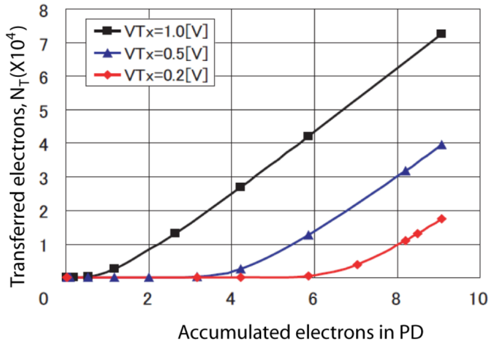
5. Non-Linearity due to Current Diffusion
A simulation to check the characteristics of partially transferred electrons,
NT with respect to the accumulated electrons in PD and
VTX has been done using the SPECTRA, a simulator built especially for simulating CMOS image sensor's pixel and CCD. The first step for simulation starts with drawing the layout in cadence and the file are transferred to the SPECTRA input file. Then, the parameters are specified and followed by running the SPECTRA in transient mode. In the simulation, the transfer time is set to 0.5 μs. The simulation results are shown in
Figure 4. From the figure, it can be said that if the accumulated electrons in PD is greater than threshold value,
QT, the transferred electrons has a linear response. However, in the region near to the
QT, it has a non-linear response due to carrier diffusion. The non-linear relation between transferred charge and potential barrier under transfer gate can be calculated by the principle of current diffusion.
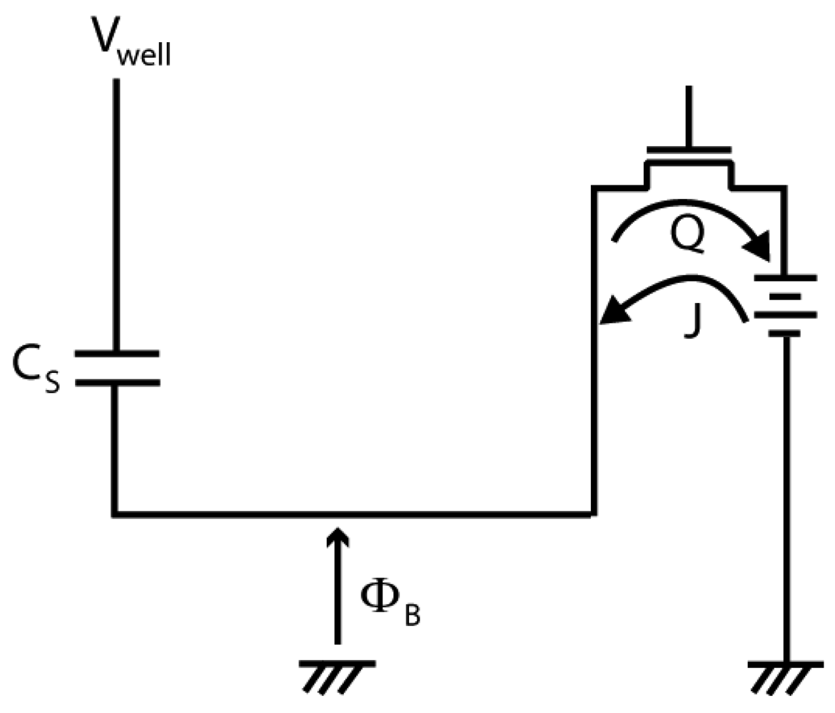
Figure 5 shows the pixels cross section and potential profile of a photodiode. The diffusion current or sub-threshold current in a semiconductor is given by:
where:
In the equation,
Dn, np, x, A and
d are the diffusion coefficient, minority carrier density, variable of diffusion length at x axis, area and depth of the channel for current flow, respectively. The
Dn is given by Einstein's relation:
δn
p/δ
x in
Equation (1) is calculated as:
where, L is the diffusion length and:
and:
Note that
ΦS is the surface potential of silicon at transfer gate and can be calculated as:
By substituting the
Equation (8) into
(7), the diffusion current can be rewritten as:
and
equation (9) can thus be simplified to:
where:
Next, the equivalent circuit shown in
Figure 6 is considered. From the figure, the current flow is given by:
Calculate the
Equation (15):
where:
and
J(0) is current at t = 0.
From
Equation (9), by assuming that
J(0) =
J(
Φbi-
ΦB = 0),
J(0) is given by:
Within the readout time, the transferred charge is given by:
If t
R = 0.5 [μs], the number of transferred electrons are:
At this time, J[0] is renamed as J1:
From the above calculations, it is clear that the charge is transferred continuously until the ΦB reach 0.455 V, then the charge transfer process stops. It also significant that the diffusion current has an exponential relationship with ΦB which suggests a non-linear relationship between transferred charge and potential barrier under the transfer gate.
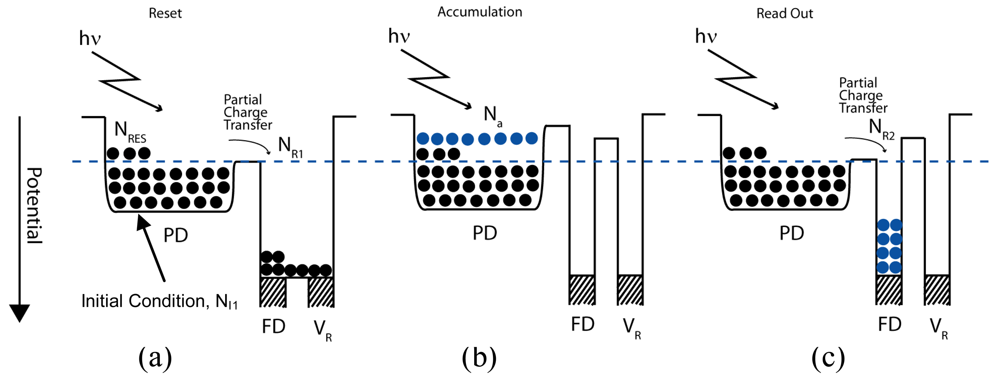
6. Non-Linearity Due to Initial Condition of a Photodiode and Its Influences on the Dynamic Range Expansion
The initial condition of the photodiode can influence the partially transferred charge for the short accumulation time signal. The Initial condition is indicated by the number of initially accumulated electrons in PD,
NI1.
Figure 7 illustrates the partial charge transfer with different initial condition of photodiode. From the figure, when a photodiode with initial condition of 17,000 electrons is partially reset, and the number of drained electron,
NR1 is 2,200, some electrons above threshold value
QT, NRES still remains in photodiode. Then, the re-accumulation operation takes place again and if the number of re-accumulated electron
Na is 2,200, the read out short accumulation time signal,
NR2 in
Figure 7 (c) should be the same as
Na. Therefore, the relation between
NR1, Na and
NR2 can be conclude as:
and:
The relationship between
NR1, Na and
NR2 of
Equation (30) can contribute to the readout error in the short accumulation signal of the sensor.
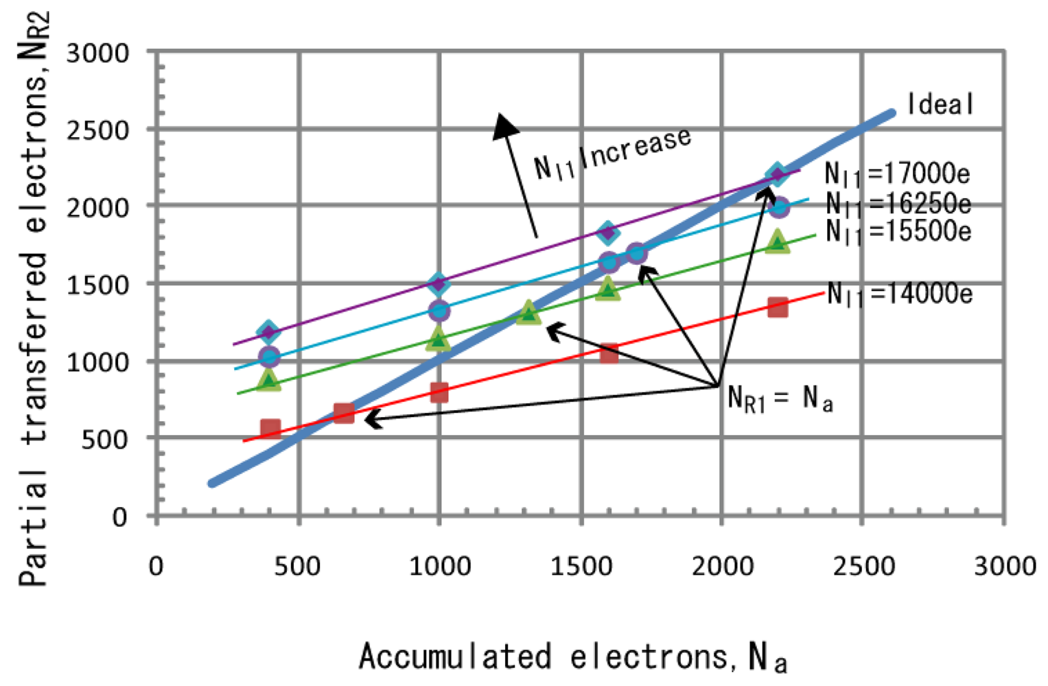
An analysis of the non-linearity due to the partial charge transfer has been conceded. A simulation is carried to check the relations of re-accumulated electrons and partially transferred electrons with respect to the initial conditions of the photodiode. In the simulation, the transfer gate drive voltage and charge transfer time is set to 0.5 V and 1.0 μs, respectively. The simulation results are shown in
Figure 8, which shows the relationship between
NR2 and
Na, deviates from the ideal curve. As the number of initially accumulated electrons in PD,
NI1 is increased, the
NR2 -
Na curve moves upward which means the error for low number of accumulated electron is increased.
The simulated relationship between
NR2 and
Na which deviates from the ideal curve can contribute to the non-linearity in the synthesized wide dynamic range signal.
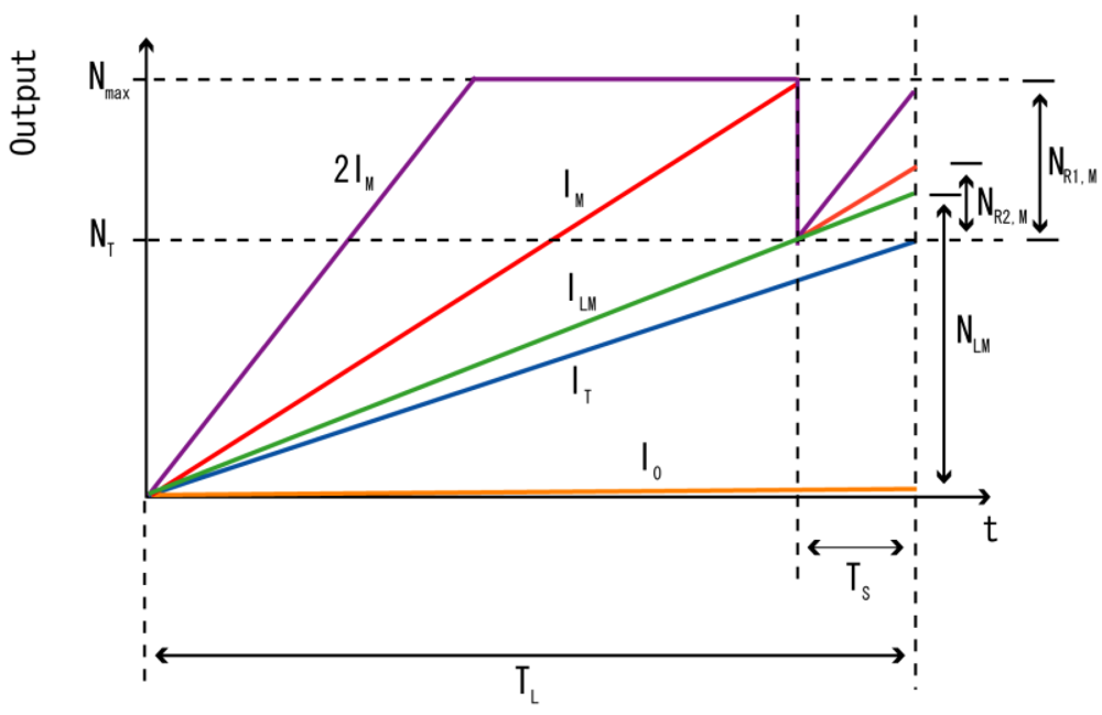
Figure 9 shows some conditions of incident light,
I0, IT, ILM, IM and
2IM during the accumulation of one frame. From the figure, some equations can be derived as:
where,
TL and
TS are the long and short accumulation time, respectively. Then, the short accumulated signal,
qNa, and the saturation level of accumulated signal,
Nmax for incident light of
IM can be written as:
For example, if
Nmax is set to 17,000 electrons and the ratio of
TL and
TS is set to 21:1, the
Na is equal to 850 electrons and by referring to the simulation results in
Figure 9, the read out electron,
NR2, at
Na equals 850 electrons, is simulated to be 1,400 electrons, different from the ideal value of 850 electrons by almost 65%. A calculation has been done from the simulation data of
Figure 8 to study the effects of changing the ratio of
TL to
TS, and the saturation level of the photodiode,
Nmax to the linearity in short accumulation signal region of wide dynamic range signals. Since, the wide dynamic range signal is synthesized from the two sets of long and short accumulation time signals using the equations:
and:
the non-linearity only affects the short accumulation signal obtained from partial transferred read out.
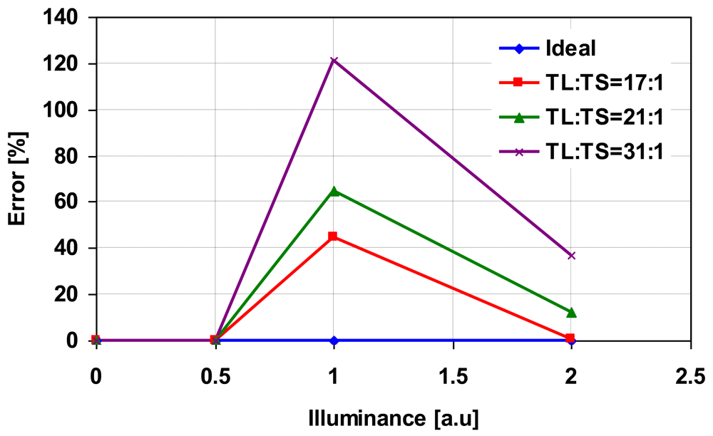
Figure 10 shows the photo-electric conversion characteristics of the synthesized wide dynamic range signals with the parameter of the ratio of
TL to
TS is set to 17:1, 21:1 and 31:1. In the calculation,
Nmax is set to 17,000 electrons. As the ratio of
TL to
TS is greater, non-linearity at high illumination region becomes worst. The error explained in percentages is shown in
Figure 11. The error is increased as the ratio of
TL to
TS is increased because
Na is decreased due to shorter accumulation period and from the simulated results in
Figure 8, the error at lower numbers of
Na is higher than the error at high numbers of
Na.
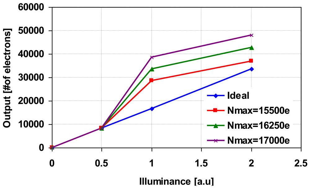
Figure 12 shows the photo-electric conversion characteristics of the synthesized wide dynamic range signals with the parameter of
Nmax set to 15,500 electrons, 16,250 electrons and 17,000 electrons. In the calculation, the ratio of
TL to
TS is set to 31:1. When
Nmax is large, non-linearity at high illumination region becomes worst. The error explained in percentages is shown in
Figure 13. As
Nmax increases, the line in
Figure 8 moves upwards, therefore despite the same
Na, the error is larger for
Na with higher
Nmax. From this analysis, it is concluded that the error increases as
Nmax increases. The dynamic range expansion ratio,
RDE, in this technique is given by:
Therefore, the dynamic range in this technique can be expanded either by using a photodiode with higher
Nmax or by increasing the ratio of
TL to
TS. However, as discussed, the higher
Nmax and ratio of
TL to
TS contributes to higher error in high illumination region, result in non-linearity in the synthesized wide dynamic range signals. Thus, the optimized
Nmax and the ratio of
TL to
TS must be considered to reduce this error for obtaining a linear response in the synthesized wide dynamic range signals. Furthermore, solutions such as double mid-point shutter technique [
7] may be applicable for reducing this error.


