Article

A Microsystem Based on Porous Silicon-Glass Anodic Bonding for Gas and Liquid Optical Sensing

by
Luca De Stefano
1,*,
Krzysztof Malecki
1,
Francesco G. Della Corte
2,
Luigi Moretti
2,
Ilaria Rea
1,
Lucia Rotiroti
1 and
Ivo Rendina
1
1
Institute for Microelectronics and Microsystems, National Council of Research, Via P. Castellino 111, 80131 Naples, Italy
2
DIMET “Mediterranea” University of Reggio Calabria, Località Feo di Vito, 89060 Reggio Calabria, Italy
*
Author to whom correspondence should be addressed.
Sensors 2006, 6(6), 680-687; https://doi.org/10.3390/s6060680
Submission received: 15 March 2006 / Accepted: 22 June 2006 / Published: 23 June 2006

Abstract

:
We have recently presented an integrated silicon-glass opto-chemical sensor for lab-on-chip applications, based on porous silicon and anodic bonding technologies. In this work, we have optically characterized the sensor response on exposure to vapors of several organic compounds by means of reflectivity measurements. The interaction between the porous silicon, which acts as transducer layer, and the organic vapors fluxed into the glass sealed microchamber, is preserved by the fabrication process, resulting in optical path increase, due to the capillary condensation of the vapors into the pores. Using the Bruggemann theory, we have calculated the filled pores volume for each substance. The sensor dynamic has been described by time-resolved measurements: due to the analysis chamber miniaturization, the response time is only of 2 s. All these results have been compared with data acquired on the same PSi structure before the anodic bonding process.

Introduction

The physical and structural properties of porous silicon (PSi), first of all its high surface area matrix, have led many scientific researchers to investigate this material, using it as a transducer in sensing systems. In particular, high sensitivity results have been obtained by monitoring changes in optical properties, such as photoluminescence [1], reflectivity [2-3] and ellipsometry [4]. Both monolayers, which act as Fabry-Perot interferometers, and multilayer devices, like Bragg filters and optical microcavities, can be easily fabricated and exploited in optical sensing experiments. The integration of sensitive elements into complex microsystems, i.e. lab on chip or micro-total-analysis systems, is of straightforward interest, especially for the miniaturisation of each component. This step is never a trivial one: the fabrication process often requires high temperatures and mechanical stresses which can damage or even destroy the bio- or chemo- sensitive transducer structures.
The anodic bonding (AB) is a standard IC fabrication technique which is widely used in microfluidic due to a wide spectrum of advantages among which the hermetic sealing [5-6]. Due to the good bonding quality, glass transparency, technological cleanness and high passivity to most of chemicals and biological substances, AB is also commonly exploited in the fabrication of lab-on-chip devices. The compatibility of this primary integration technique with highly demanding sensing micro-components plays a basic role in view of the realization of lab-on-chip devices. We have recently reported on the optimisation of the standard silicon-glass AB parameters, searching for low temperature, low voltage and short time, taking into account the electrode type and thickness of glass wafers [7].
In the present work, the above mentioned results have been exploited and combined with new bonding findings, to ensure AB compatibility with the features of porous silicon (PSi) transducer. We have studied the static and dynamic sensor response on exposure to vapours of several organic compounds. The results have been compared with those obtained for the same PSi layer before the integration process.

Theory

Even if we have already realised μ-chambers with porous silicon multilayer optical structures, such as Bragg filters and optical microcavities which are more performing in terms of sensitivity and resolution, in this first optical characterisation, we have followed the approach of Sailor et al. [2] choosing the simple case of a single layer of porous silicon as our transducer device. Figure 1 shows a typical reflectivity spectrum from a PSi layer under white light illumination.
From the optical point of view, this structure is an optical Fabry-Perot interferometer, so that the maxima in the reflectivity spectrum appear at wavelengths λm which satisfy:
m = 2 n d / λ m
where m is an integer, d is the film thickness and n is the average refractive index of the layer [8-9]. If we assume that the refractive index is independent on the wavelength over the considered range, the maxima are equally spaced in the wavenumber (1/λm). When the maximum order m is plotted as a function of the wavenumber, each point lies on a straight line which slope is the optical path, as it is shown in the inset of Fig. 1. When the PSi layer is exposed to vapors, or dip in the liquid phase of the same substance, the substitution of air in the pores by its molecules causes a fringes shift in wavelength, which corresponds to a change in the optical path nd. Since the thickness d is fixed by the physical dimension of the PSi matrix, the variation is clearly due to changes in the average refractive index. In the case of vapors and gases, the filling liquid phase is due to the capillary condensation phenomenon, which is regulated from the Kelvin equation:
K B T ρ l ln ( p sat / p ) = 2 γ lg cos θ / R
where ρl is the density of the liquid phase, γlg is the liquid-gas surface tension coefficient at room temperature T, R is the radius of the pores, p/psat is the relative vapor pressure into the pores, and θ is the contact angle [10].
A quantitative model taking into account the optical path increase can be realized by applying the Bruggemann effective medium approximation theory. The relation between the volume fraction of each medium and its dielectric constant can be written as:
( 1 p ) ( ɛ S i ɛ p ɛ S i + 2 ɛ p ) + ( p V ) ( ɛ air ɛ p ɛ air + 2 ɛ p ) + V ( ɛ c h ɛ p ɛ c h + 2 ɛ p ) = 0
where p, V, εsi, εair, εch and εp are the layer porosity, the layer liquid fraction (LLF), the dielectric constants of silicon, air, chemical substance and porous silicon, respectively [11].

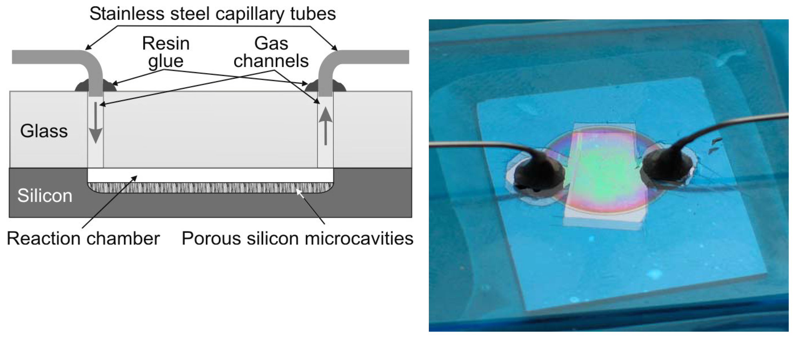
Experimental Section

We have designed and fabricated a sensor device which can be considered the basic element of a lab-on-chip, just integrating PSi, as the transducer material, and a glass slide, which ensures sealing and the interconnections for fluids inlet and outlet. The silicon wafer used in this work is a p+ type, <100> crystal orientation, with a resistivity of 8-12 mΩcm. The glass is a Borofloat 33 type, 1 mm thick. The reaction microchamber has been realized by a two-step electrochemical etching. The first step is a high current density (800 mA/cm2 for about 300 s) electrochemical etch in hydrofluoric acid and ethanol (HF:EtOH/50:50) solution which creates a μ-well (100 μm deep) in the bulk silicon. The second step is a consecutive electrochemical etch which is used to fabricate the PSi layer at the bottom of the μ-chamber. The process parameters for this last step were: current density of 400 mA/cm2 and etching time of 3.2 s. More details on μ-chamber fabrication can be found elsewhere [12]. The thickness and porosity of the PSi layer was measured by variable angle spectroscopic ellipsometry using a Horiba-Jobin-Yvon UVISEL ellipsometer. After the mechanical drilling of the flow channels, the glass slide has been cleaned and activated for the AB process following standard RCA and H2O2 procedures. Because of the highly reactive PSi nature, the standard cleaning procedures had to be changed with a soft cleaning procedure based on trichloroethylene, acetone and ethanol. The silicon chip has also been carefully rinsed in deionized water for several minutes. Silicon etched wafer and glass top prefabricated components have been anodically bonded together with mutual alignment: a successful bonding, in terms of mechanical strength and bond quality, has been obtained at a temperature of 200°C, voltage of 2.5 kV, with a process time of 1.5 minutes. The cross section of the chip structure and the general-view of the real device are shown in Figure 2. The reflectivity spectra in the VIS-IR wavelength region have been recorded with a very simple experimental set-up: a white source illuminates, through an optical fiber and a collimator, the porous silicon at nearly normal incidence. The reflected light is collected by an objective and coupled into a multimode fiber. The signal is directed in an optical spectrum analyzer (Ando, Mod. AQ-6315B) and measured with a 0.2 nm resolution. We have also performed time-resolved measurement in order to characterize the sensor dynamic: using the laser beam from an IR source, we have measured, as a function of time, the signal of a receiving photodetector before, during and after the exposure to acetone.

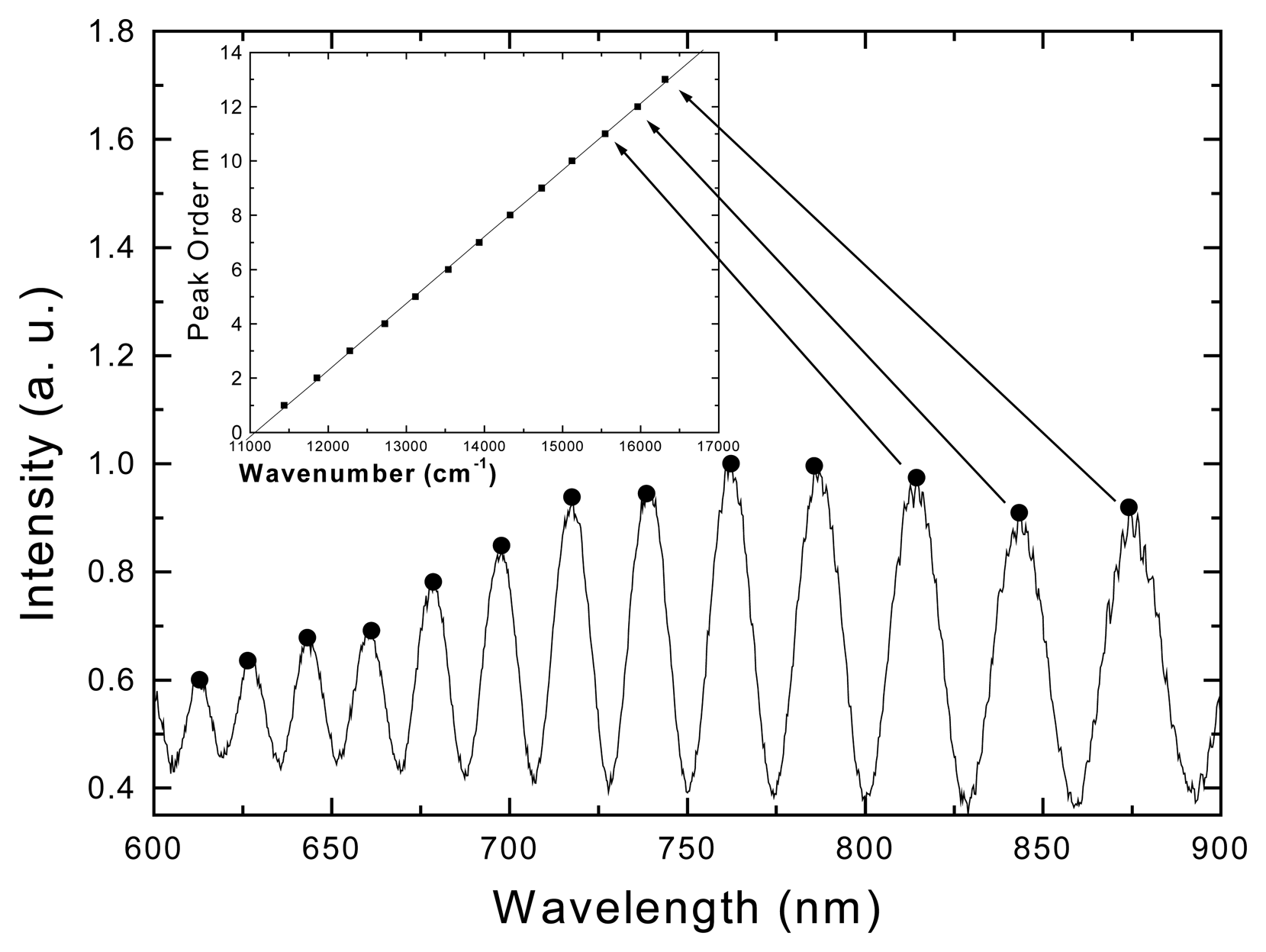
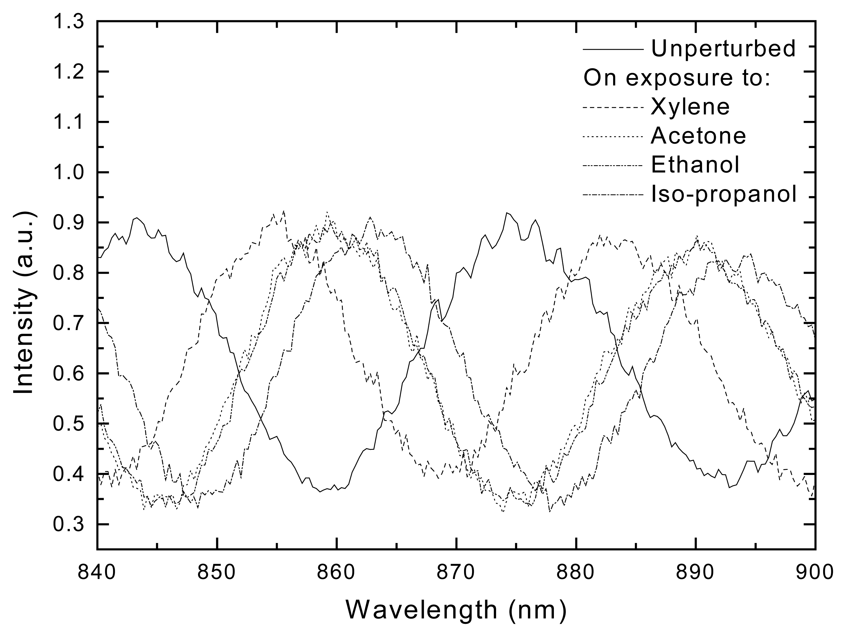
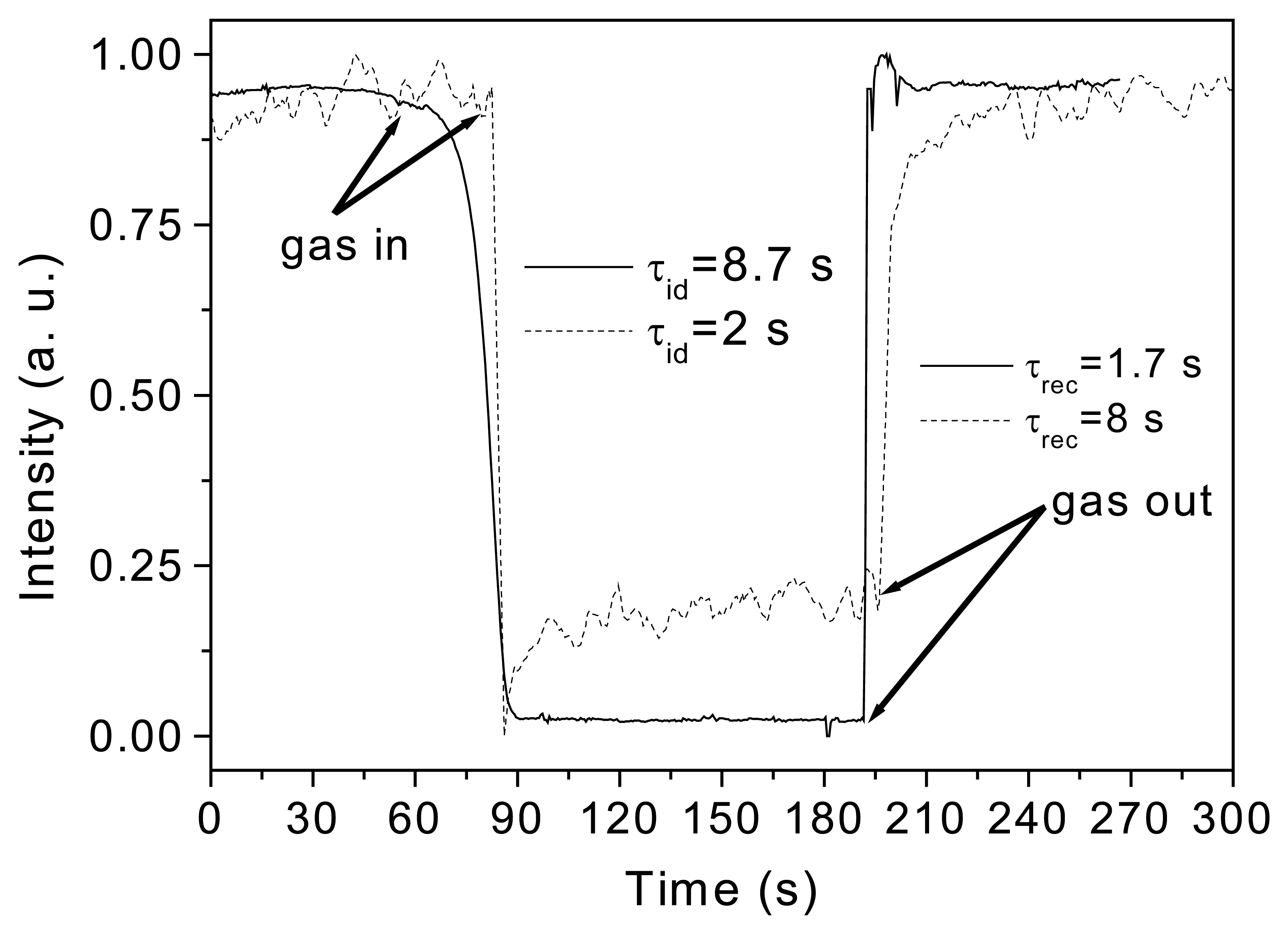
Results and Discussion

From the ellipsometric measurements we have estimated the thickness and the porosity of the porous silicon sensitive layer, resulting in about 9.1 μm and 79 %, respectively.
Using the Bruggemann relation in Eq. (2), the refractive index is calculated as 1.34. As it can be noted in the reflectivity spectra reported in Figure 3, on exposure to several volatile substances in non-saturated atmosphere, due to the phenomenon of capillary condensation, the average refractive index of the layer increases, and, as a consequence the optical thickness of the porous silicon layer also increases.
In Figure 4 the maxima of order m as function of wavenumber are shown; the slopes of the lines give the optical thickness of the layer for each substance. In the wavelength range considered, the assumption of a refractive index independent on the wavelength is satisfied since the PSi refractive index changes less then 2 % in this interval. Using the Eq. (3), the LLF, which is the filled volume by the condensed liquid, has been calculated for each substance obtaining the values reported in Table 1. The LLF values are about 30 % lower than ones obtained in the case of the PSi transducer before of the AB process [13]. These differences can be ascribed to a slight oxidation of the porous silicon layer due to the AB temperature process.
The silicon oxide can fill or obstruct the very small pores of the sponge-like structure, preventing the liquid to condense into them. Moreover, due to the air present during the AB process, there probably exists an extra pressure into the μ-chamber because some air has been entrapped in the PSi matrix. As a consequence, according to the Kelvin Equation (2), the capillary condensation of the liquid phase decreases.
The result of time-resolved measurement is compared in Figure 5 to the data acquired on the same PSi layer before the AB integration process: it is well evident that, due to chamber miniaturization, the identification time (τid=2 s) is significantly shorter.
The values of response time depends not only on the physical phenomena involved (i.e., equilibrium between adsorption and desorption in the PSi layer) but also on the geometry of the test chamber and on the measurement procedure, i.e. static or continuous flow mode. In static condition, the identification time is mainly determined by the diffusion of the gas into the chamber volume: in fact, when vapor is in contact with the porous silicon surface, the capillary condensation takes place instantaneously [14-15]. For the same reason, the recovery time is longer (τrec=8 s): as soon as Nitrogen is introduced into the μ-chamber, the conditions for capillary condensation are not still valid so that the liquid phase disappears, depending on atmosphere rate exchange. As it is shown in this graphic, the sensor response is completely reversible.

Conclusions

In this work, we have optically characterized an original hybrid silicon-glass sensor system, based on PSi and AB technologies, which can be thought as the reaction chamber of a more complex lab-on-chip. Reflectivity spectrum of the device has been studied on exposure to vapors of organic volatile solvents. An increase of the optical path, due to capillary condensation of the vapor into the pores, has been observed. Using the Bruggemann effective medium approximation we have calculated the liquid volume fraction adsorbed into the layer for each substance, obtaining values between 0.22 and 0.23. We have characterized the sensor dynamic by time-resolved measurement during exposure to acetone. The data assure fast analysis time and the complete reversibility of the sensing mechanism. The comparison with data obtained from the same PSi transducer before the AB, shows that the integration process did not degrade the sensor features.

Acknowledgments

This work has been supported by Marie Currie Fellowship of the European Community programme “Technologies for micro-opto-mechanical systems” under contract number CO-IMM-NA-01-2002.

References

  1. Mulloni, V.; Pavesi, L. Porous silicon microcavities as optical chemical sensors. Appl. Phys. Lett. 2000, 76, 2523–2525. [Google Scholar]
  2. Gao, J.; Gao, T.; Sailor, M.J. Porous-silicon vapor sensor based on laser interferometry. Appl. Phys. Lett. 2000, 77, 901–903. [Google Scholar]
  3. Benson, T. M.; Arrand, H. F.; Sewell, P.; Niemeyer, D.; Loni, A.; Bozeat, R. J.; Kruger, M.; Arens-Fischer, R.; Thoenissen, M.; Luth, H. Progress towards achieving integrated circuit functionality using porous silicon optoelectronic components. Mat. Sci. Eng. B. 1999, 69-70, 92–95. [Google Scholar]
  4. Wongmanerod, C.; Zangooie, S.; Arwin, H. Determination of pore size distribution and surface area of thin porous silicon layers by spectroscopic ellipsometry. Applied Surface Science 2001, 172, 117–125. [Google Scholar]
  5. Puers, B.; Peeters, E.; Van Den Bossche, A.; Sansen, W. A capacitive pressure sensor with low impedance output and active suppression of parasitic effects. Sens. Actuat. A. 1990, 21-23, 108–114. [Google Scholar]
  6. Obermeier, E. Proc. Semiconductor Wafer Bonding. Science, Technology and Applications. Electrochem. Soc. 1995, 212–220. [Google Scholar]
  7. Malecki, K.; Della Corte, F.G. Silicon-glass anodic bonding at low temperature. Proc. of Micromachining and Microfabrication Process Technology X, SPIE 2005, Vol. 5715, 180–189. [Google Scholar]
  8. Lin, V.S.-Y.; Motesharei, K.; Dancil, K.-P. S.; Sailor, M. J.; Ghadiri, M. R. A porous silicon-based optical interferometric biosensor. Science 1997, 278, 840–843. [Google Scholar]
  9. Anderson, M.A.; Tinsley-Brown, A.; Allcock, P.; Perkins, E. A.; Snow, P.; Hollings, M.; Smith, R. G.; Reeves, C.; Squirrell, D. J.; Nicklin, S.; Cox, T. I. Sensitivity of the optical properties of porous silicon layers to the refractive index of liquid in the pores. Phys. Stat. Sol. A. 2003, 197, 528–533. [Google Scholar]
  10. Neimark, V.; Ravikovitch, P. I. Capillary condensation in MMS and pore structure characterization. Microporous Mesoporous Mater. 2001, 44-45, 697–707. [Google Scholar]
  11. Spanier, J.E.; Herman, I. P. Use of hybrid phenomenological and statistical effective-medium theories of dielectric functions to model the infrared reflectance of porous SiC films. Phys. Rev. B. 2000, 61, 10437–10450. [Google Scholar]
  12. De Stefano, L.; Malecki, K.; Moretti, L.; Rendina, I. Anodically bonded silicon-glass optical chip for biochemical sensing applications. Proc. SPIE. Int. Soc. Opt. Eng. 2005. [Google Scholar]
  13. De Stefano, L.; Rendina, I.; Moretti, L.; Rossi, A.M.; Tundo, S. Smart optical sensors for chemical substances based on porous silicon technology. Applied Optics 2004, 43/1, 167–172. [Google Scholar]
  14. Allcock, P.; Snow, P.A. Time-resolved sensing of organic vapors in low modulating porous silicon dielectric mirrors. J. Appl. Phys. 2001, 90, 50525057. [Google Scholar]
  15. De Stefano, L.; Moretti, L.; Rendina, I.; Rossi, A.M. Time-resolved sensing of chemical species in porous silicon optical microcavity. Sensor and Actuators B. 2004, 100, 168–172. [Google Scholar]
Figure 1. Reflectivity spectrum of PSi layer. In the inset the m-order peak are plotted as function of the wavenumber.
Sensors 06 00680f1
Figure 2. Schematic and real view of the μ-chamber for lab-on-chip applications.
Sensors 06 00680f2
Figure 3. Reflectivity spectra of the unperturbed sensor and on exposure to vapours of organic compounds.
Sensors 06 00680f3
Figure 4. Maximum m-order as function of wavenumber (1/λm). The slopes of the straight lines are the optical thicknesses of the unperturbed layer and on exposure to the vapours.
Sensors 06 00680f4
Figure 5. Time-resolved measurements of porous silicon layer during the monitoring of acetone in 0.4 l test chamber (solid line) and in the integrated 14 μl μ-chamber (dashed line).
Sensors 06 00680f5
Table 1. Chemical organics substances used in sensing experiments and some relevant physical-chemical properties a.
Chemical compoundsnρ(g/cm3)STC (mN/m)VP (kPa)BP (°C)Δ<nd> (nm)LLF
Iso-propanol1.3770.78520.936.882.410000.22
Ethanol1.3600.78522.85.8789500.23
Xylene1.5011.45438.80.04621414000.22
Acetone1.3590.79123.4630.8569980.23
an is the liquid refractive index; ρ is the density (@ 25 °C); STC is the surface tension coefficient (@ 25 °C); VP is the vapor pressure; BP is the boiling point; Δ<nd> is the average optical path increase and LLF the layer liquid fraction.

