
Enhancement of Spurious Signal Suppression in Microstrip Mixers by Load Resistor Termination
 ,
,  , , and
Abstract
1. Introduction
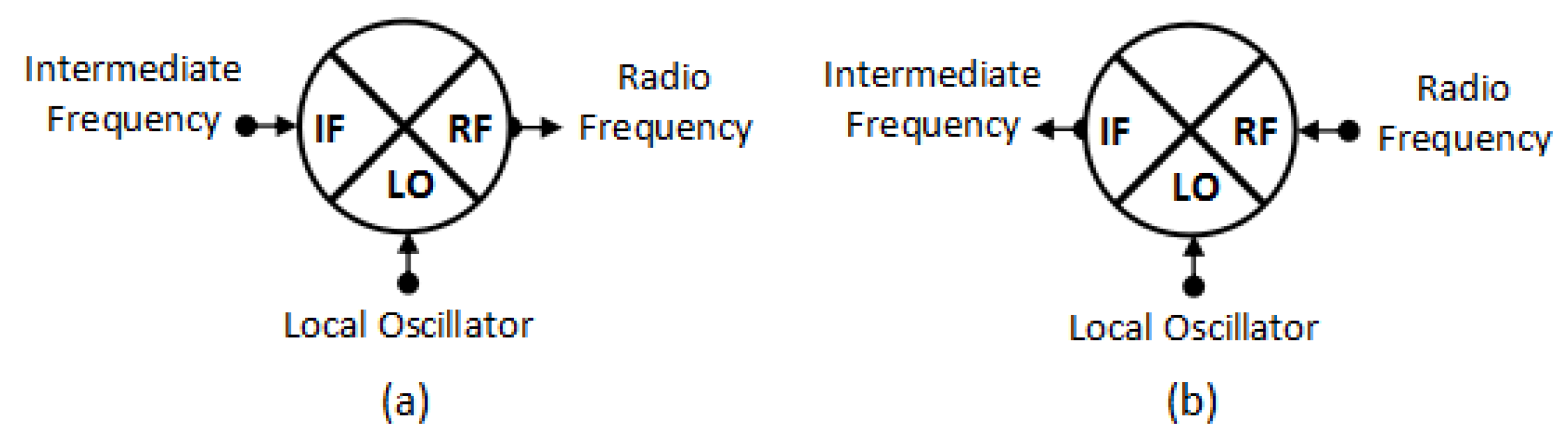
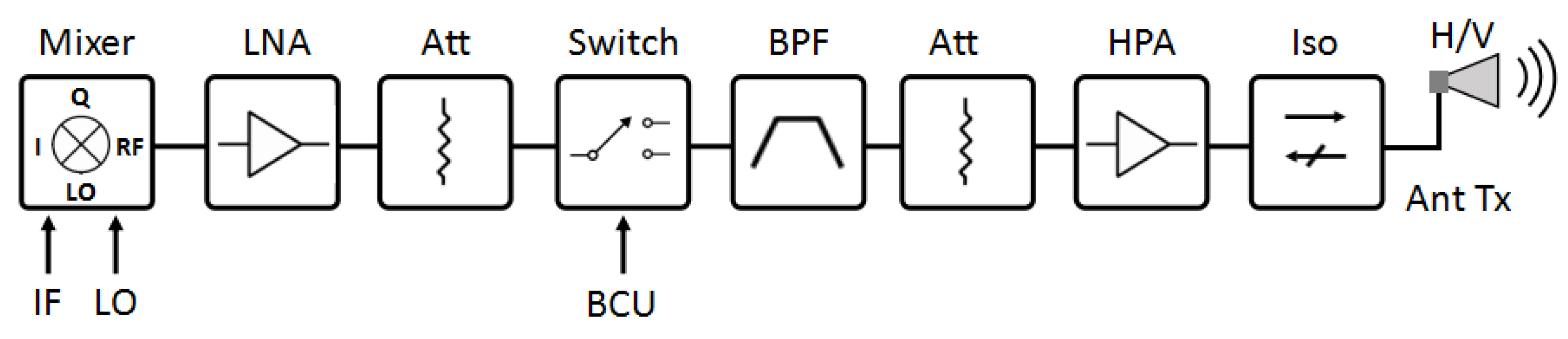
2. Basic Design
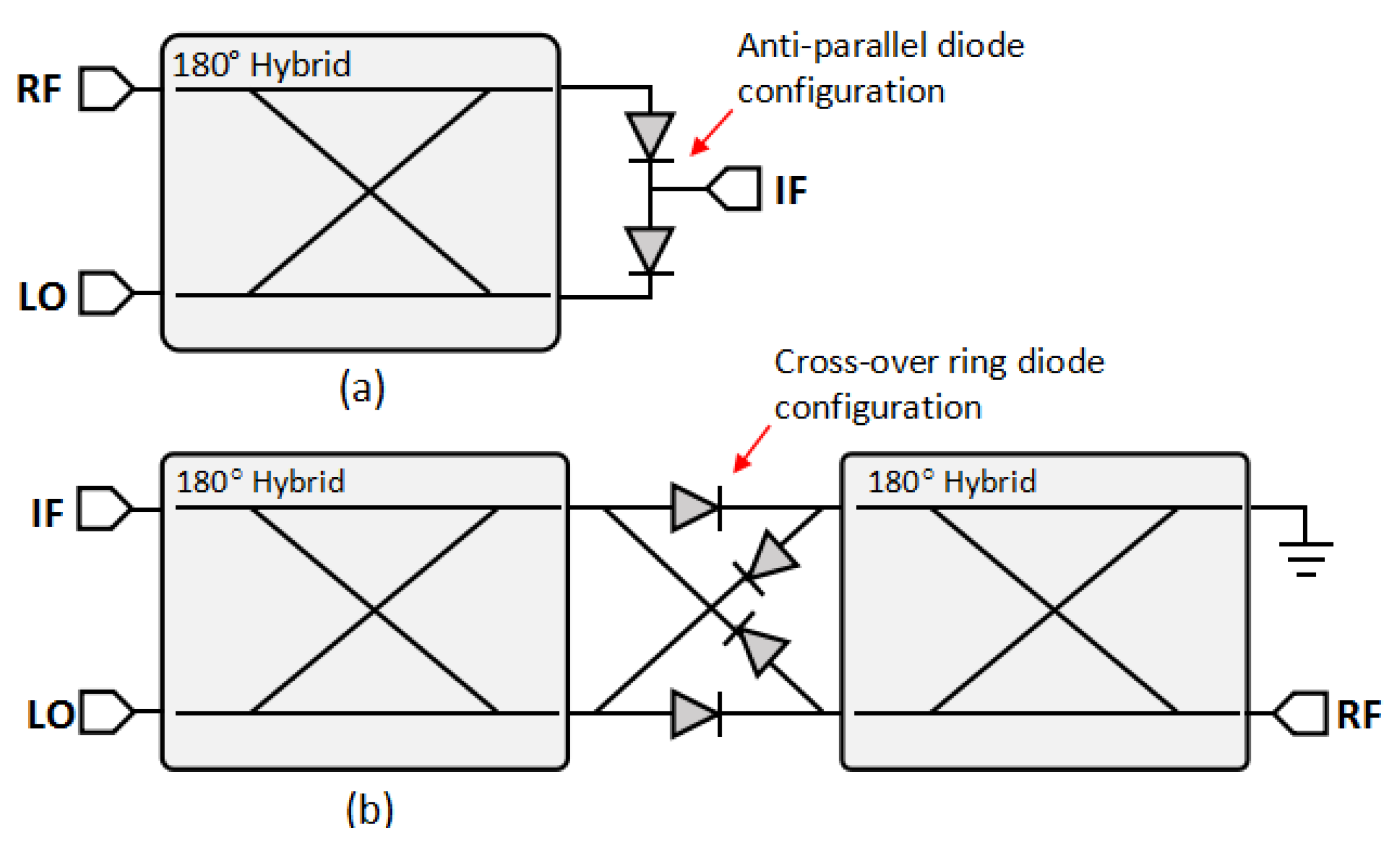
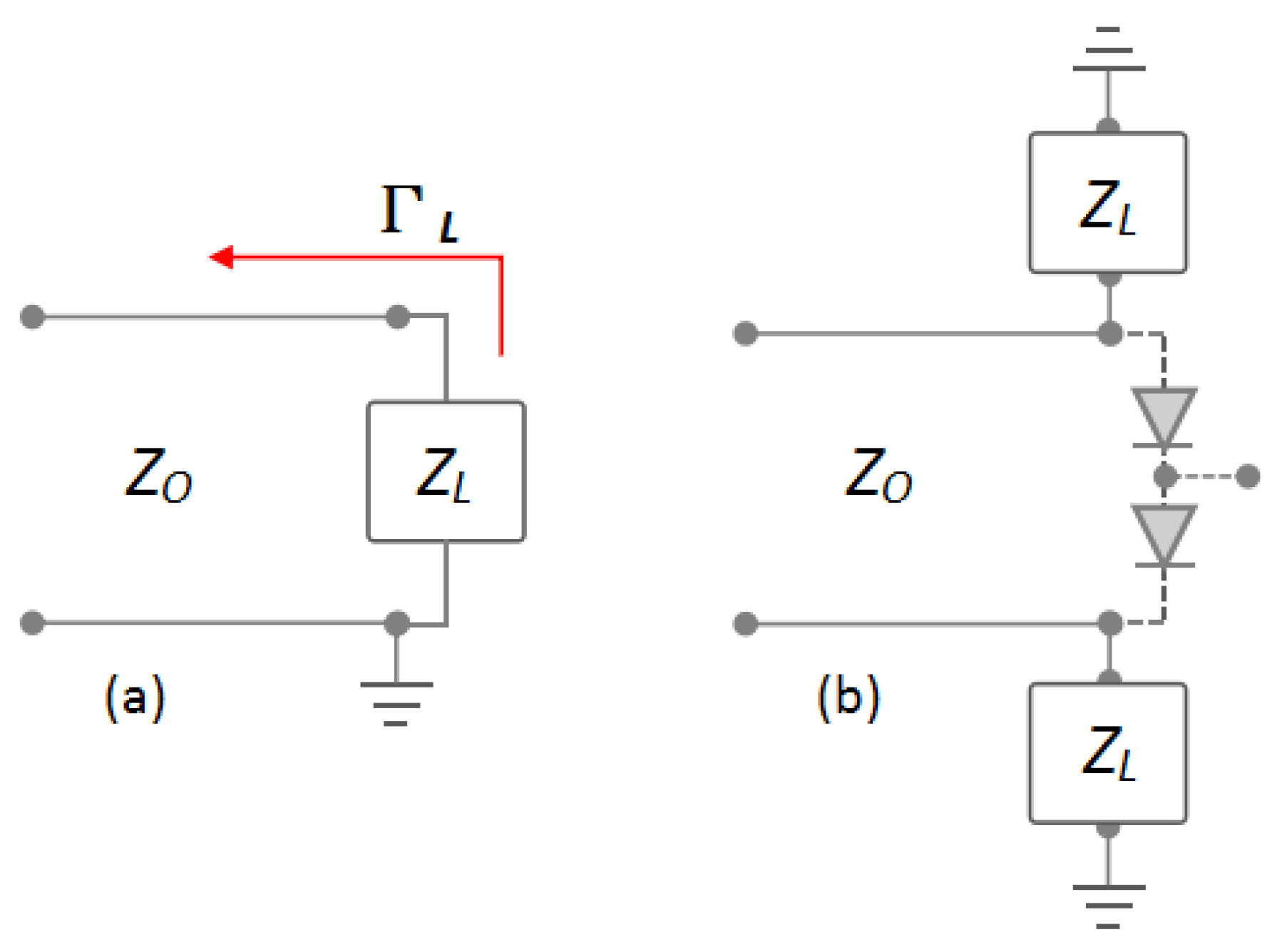
2.1. Conventional Mixer
2.2. Modified Mixer
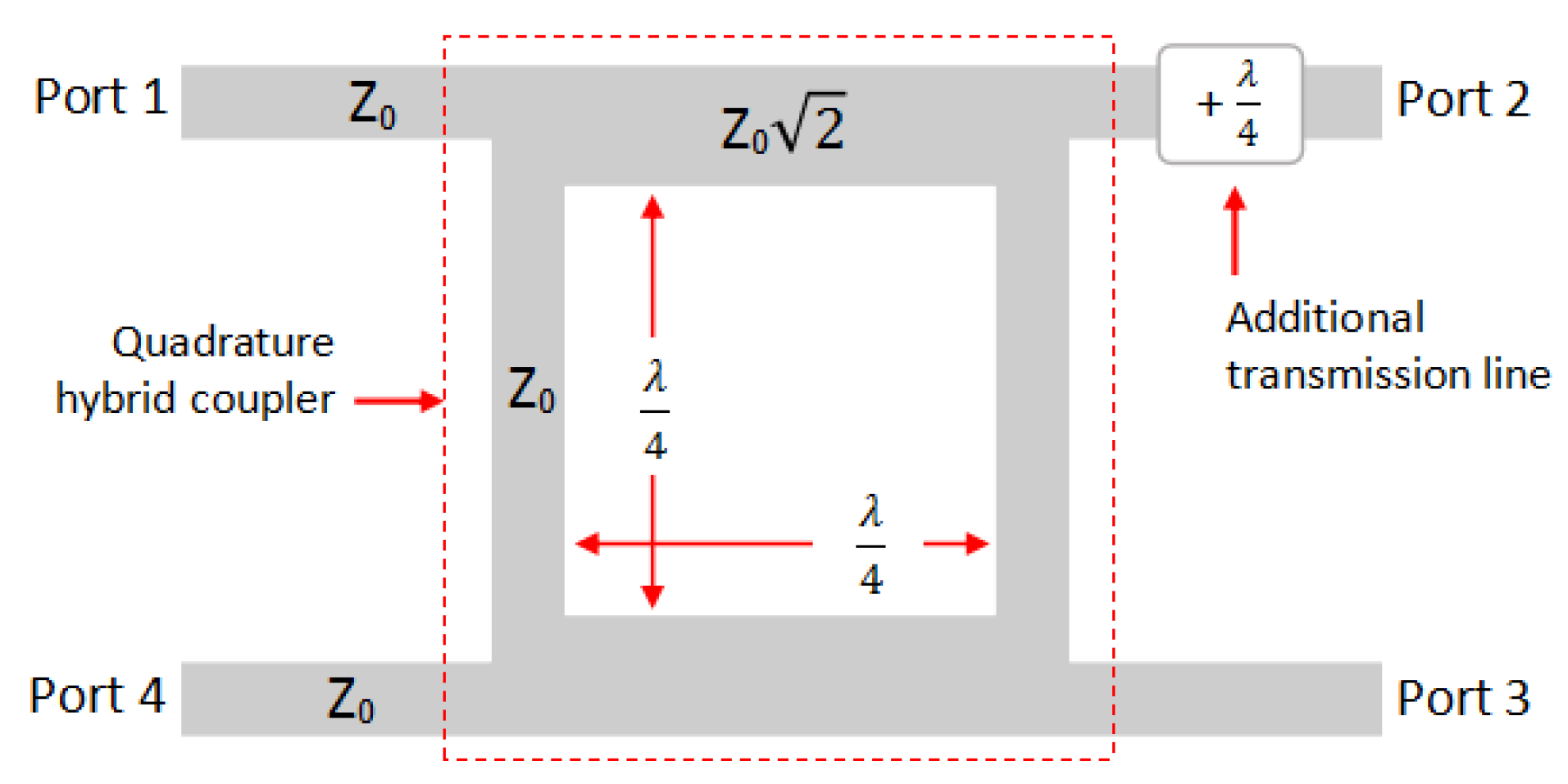
2.3. Dimension and Material
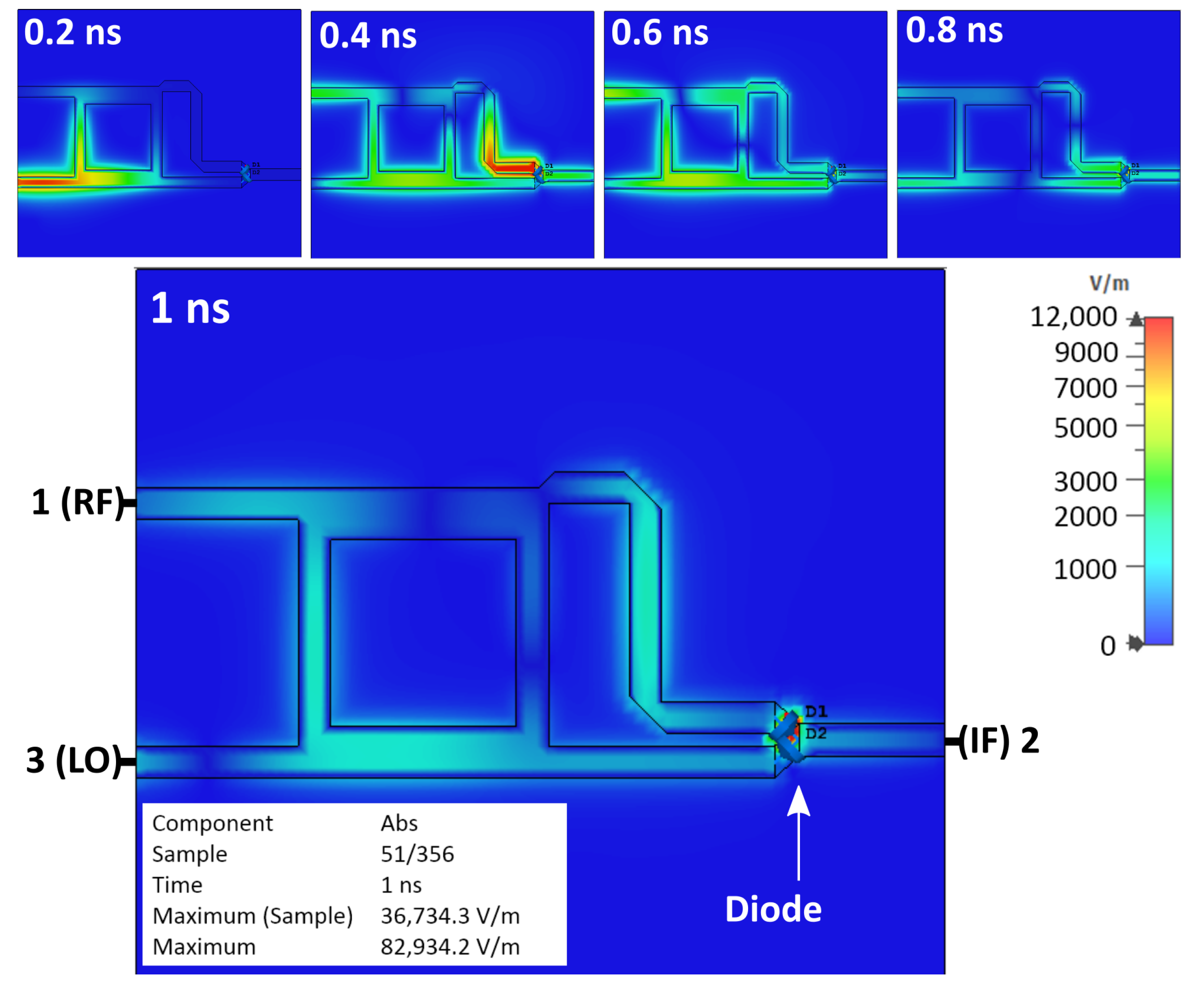
3. Simulation and Measurement
3.1. Conventional Mixer
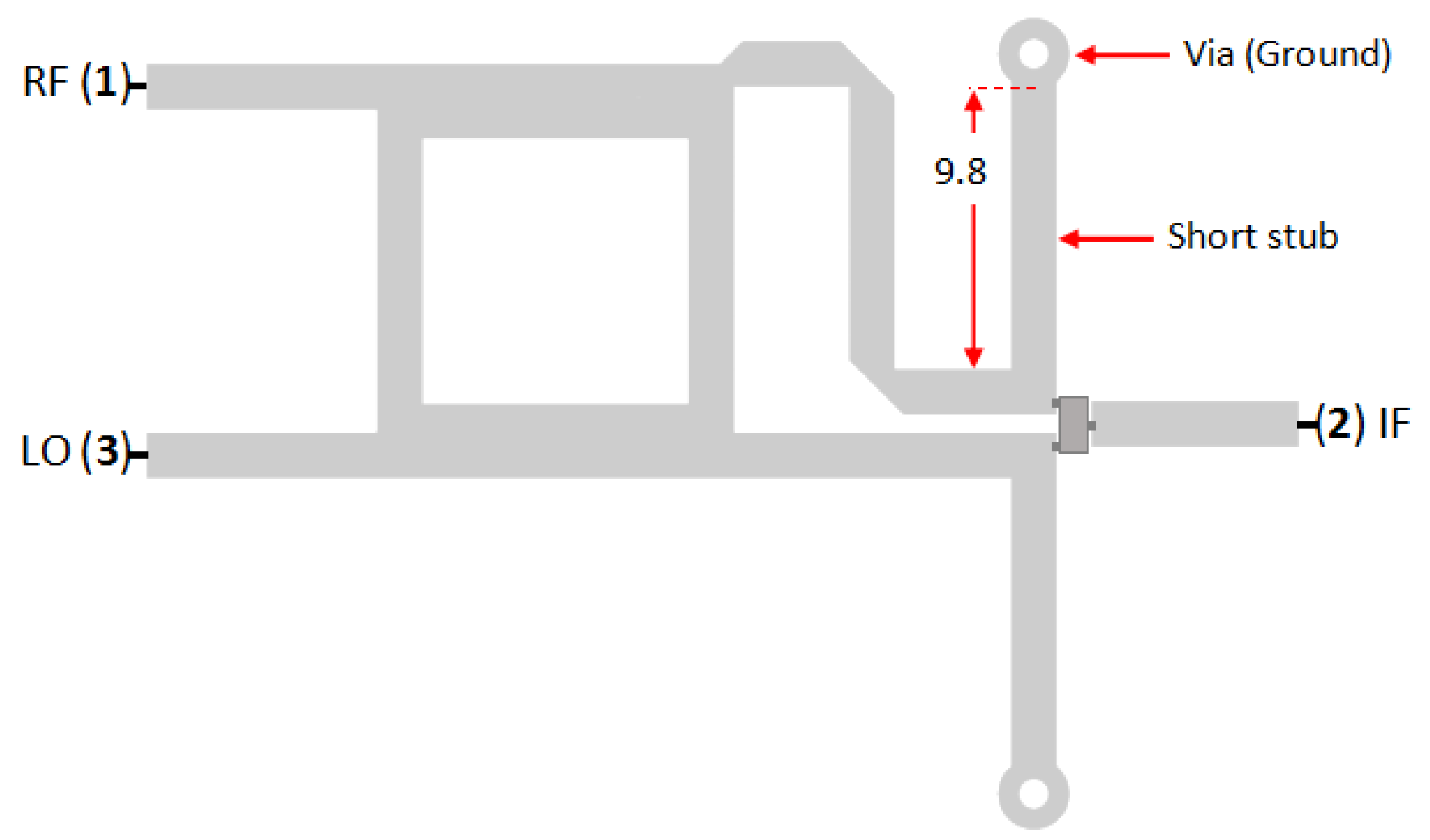
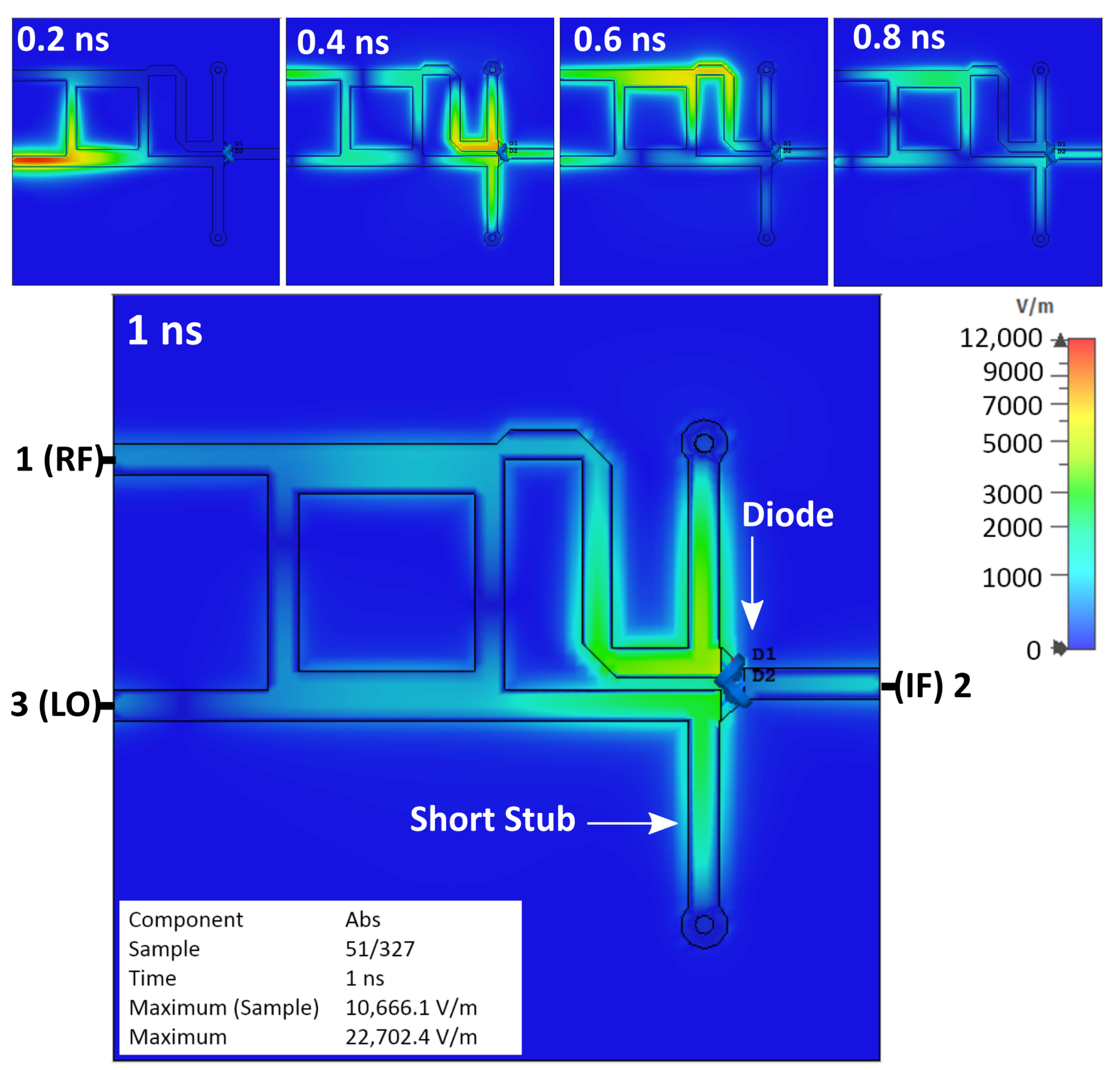
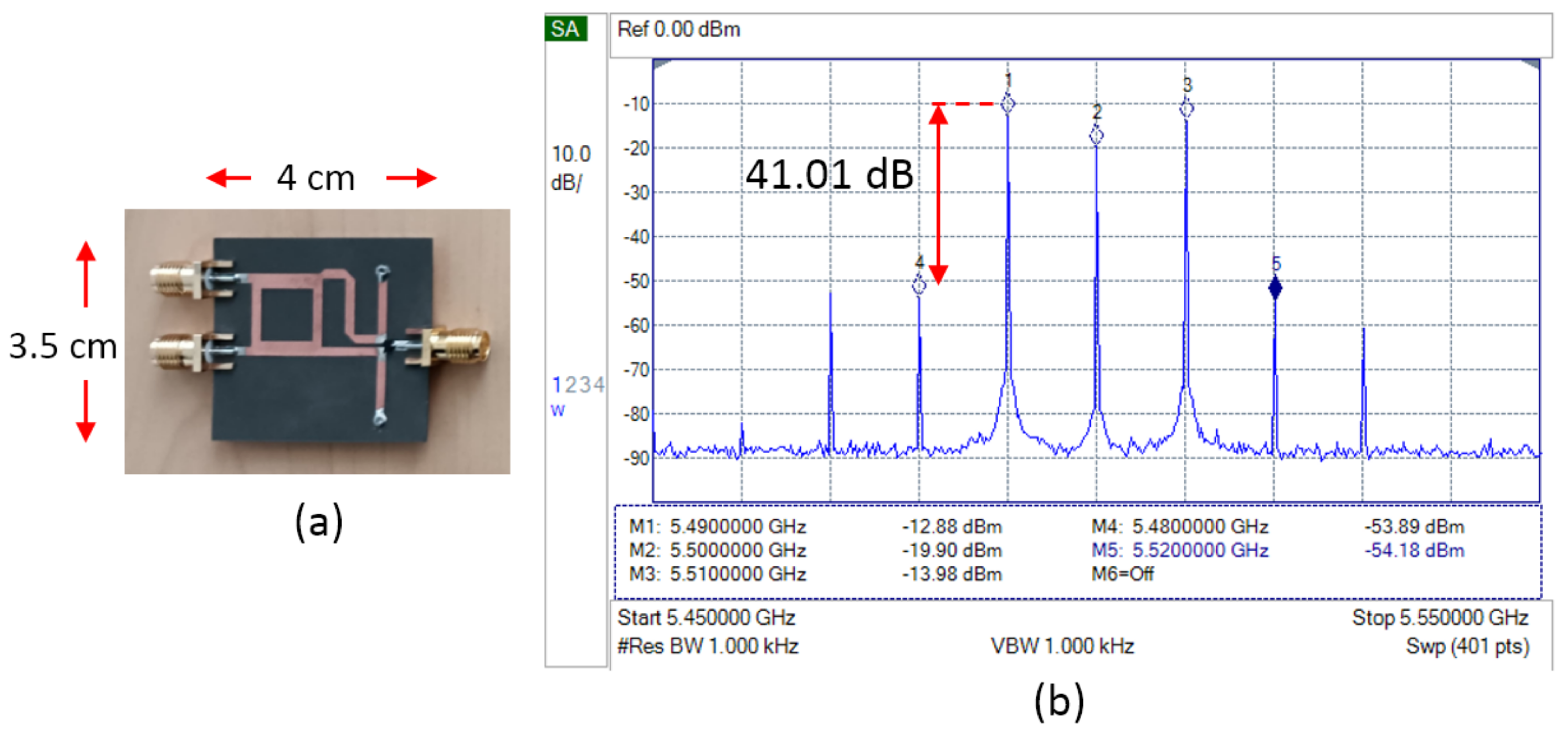
3.2. Modified Mixer (Short Stub)
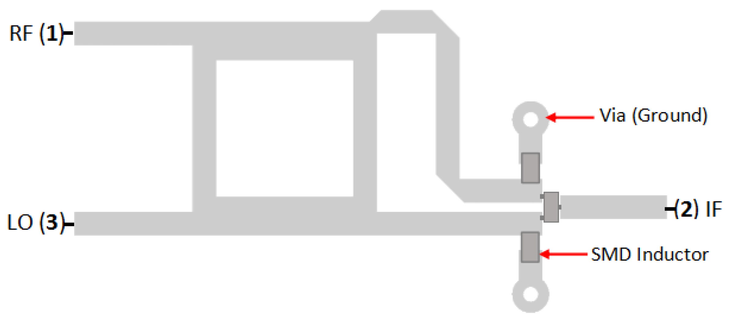
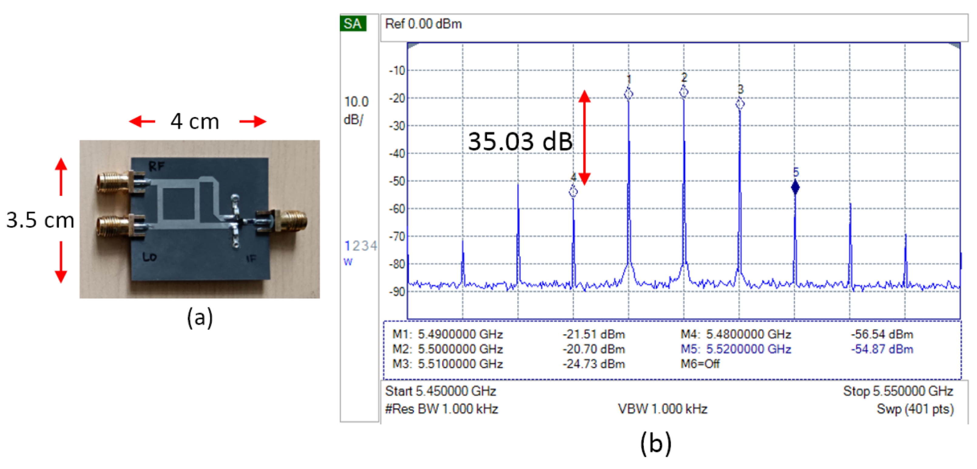
3.3. Modified Mixer (Inductor)
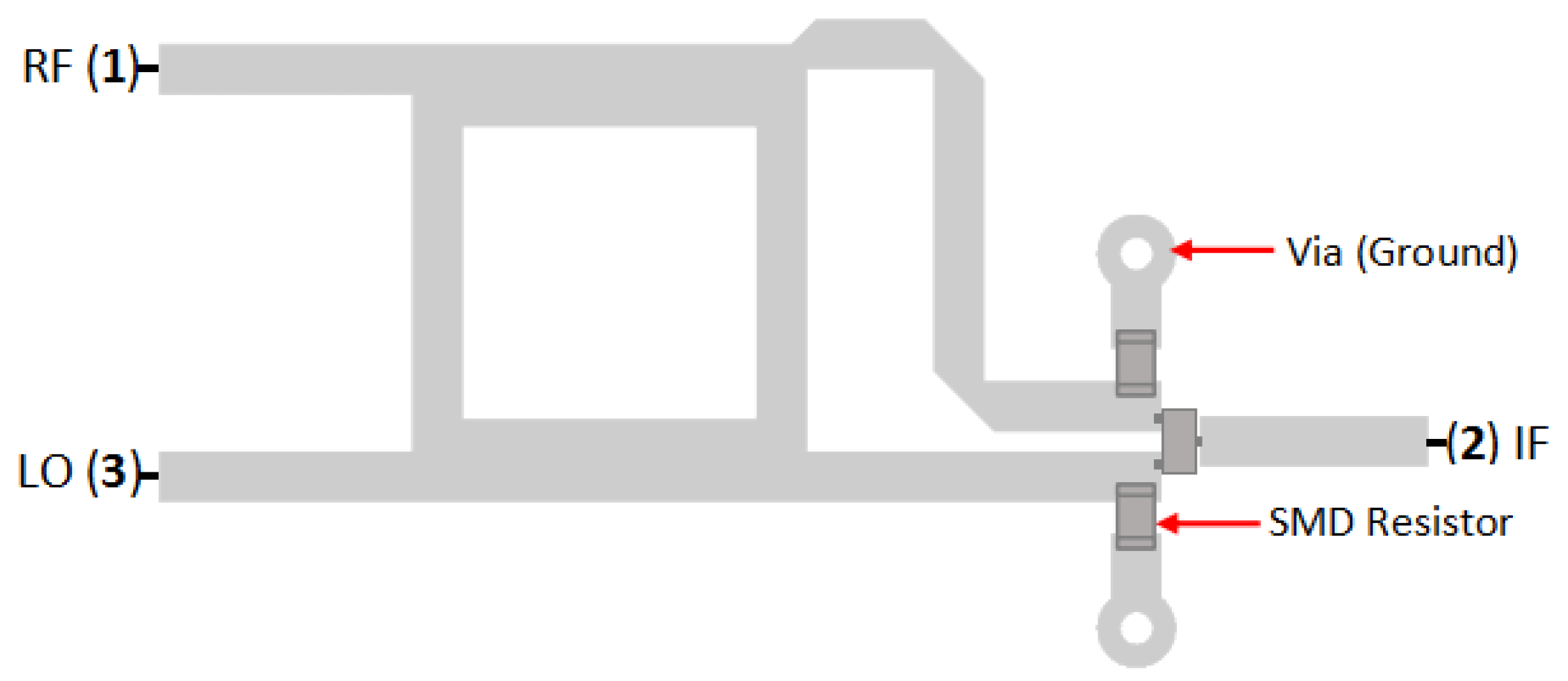
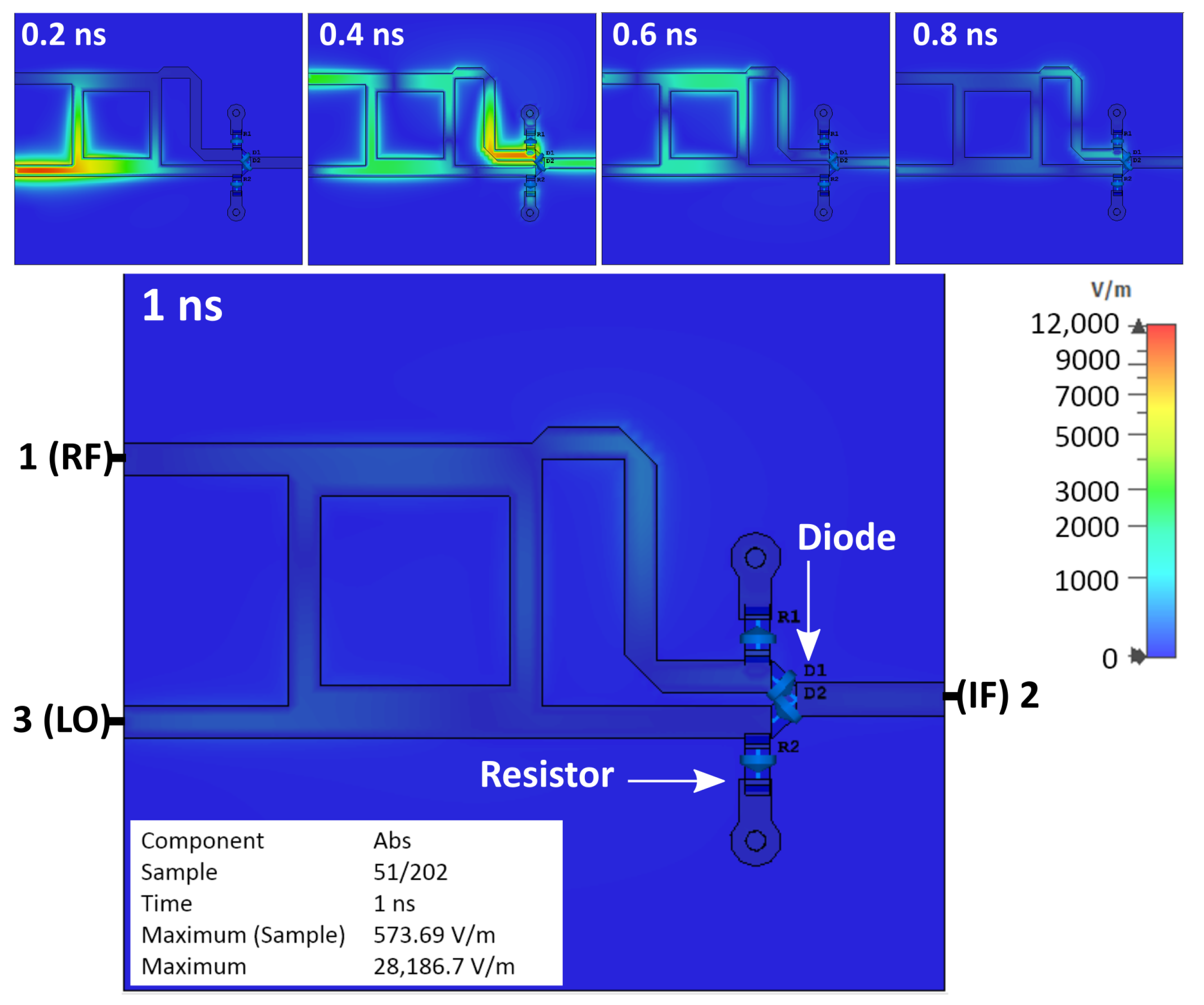
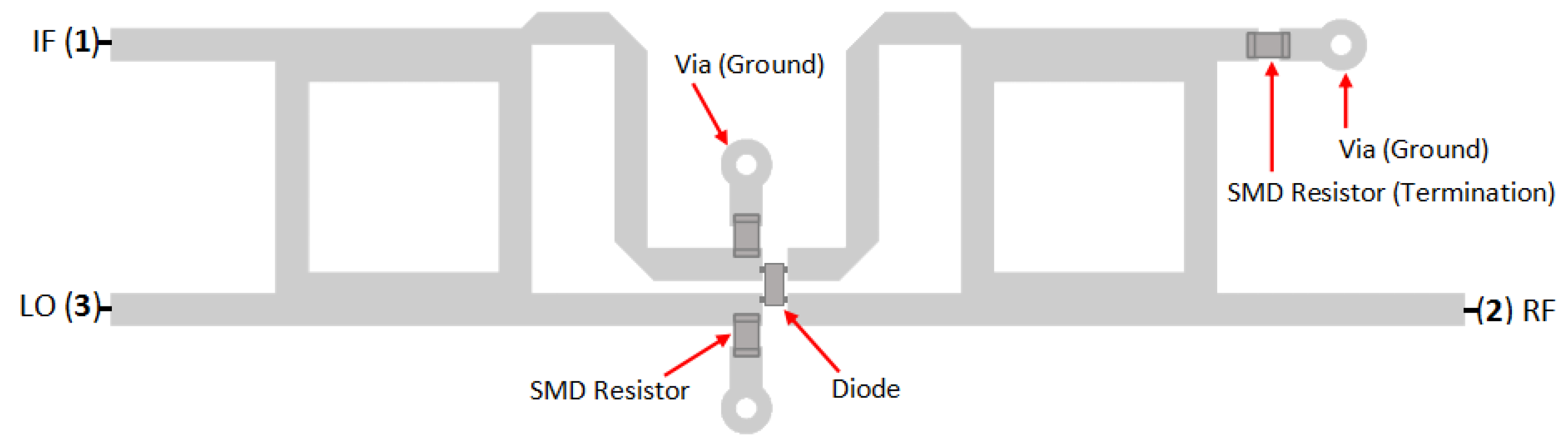
3.4. Modified Mixer (Load Resistor)
4. Discussion
Author Contributions
Funding
Data Availability Statement
Acknowledgments
Conflicts of Interest
References
- De Padova, A.; Longhi, P.E.; Colangeli, S.; Ciccognani, W.; Limiti, E. Design of a GaN-on-Si Single-Balanced Resistive Mixer for Ka-Band Satcom. IEEE Microw. Wireless Compon. Lett. 2019, 29, 56–58. [Google Scholar] [CrossRef]
- Guo, J.; Xu, Z.; Qian, C.; Dou, W.-B. Design of a Microstrip Balanced Mixer for Satellite Communication. Prog. Electromagn. Res. 2011, 115, 289–301. [Google Scholar] [CrossRef]
- Palombini, D.; Cavanna, T.; Arena, S.; Limiti, E. Design of Sub-Harmonic Mixer MMIC for EHF Satellite Links. Prog. Electromagn. Res. C 2016, 66, 149–161. [Google Scholar] [CrossRef]
- Pushpa, K.; Ghosh, J. Dual-band Subharmonic Mixer for Wifi Application with Improved Conversion Loss and RF-to-IF Isolation. PIER C 2021, 112, 11–20. [Google Scholar] [CrossRef]
- Cidronali, A.; Pagnini, L.; Collodi, G.; Passafiume, M. A Highly Linear Ka-Band GaN-on-Si Active Balanced Mixer for Radar Applications. IEEE Trans. Circuits Syst. I 2022, 69, 4453–4464. [Google Scholar] [CrossRef]
- Zeng, J.J.; Lin, X.Q.; Su, Y.H.; Yang, Y.M.; Mei, P.; Zhu, Z.B. Low-Cost Third-Harmonic Mixer for W-Band Retrodirective System Applications. IEEE Microw. Wirel. Components Lett. 2022, 32, 1323–1326. [Google Scholar] [CrossRef]
- Rosu, I. RF Mixer. Available online: https://www.qsl.net/va3iul/RF%20Mixers/RF_Mixers.pdf (accessed on 12 March 2024).
- Marki, F.; Marki, C. Mixer Basics Primer: A Tutorial for RF Microwave Mixers. Available online: https://markimicrowave.com/assets/c2c4688b-15c7-4421-a703-254cb238f9fb/Mixer_Basics_Primer.pdf (accessed on 11 September 2023).
- Pozar, D.M. Microwave Engineering, 4th ed.; John Wiley & Sons Inc.: Hoboken, NJ, USA, 2012; pp. 637–658. [Google Scholar]
- Infineon. Schottky Diode Mixer for 5.8 GHz Radar Sensor. Available online: https://www.infineon.com/cms/en/product/rf/rf-diode/rf-mixer-and-detector-schottky-diode/#!?fileId=5546d46265f064ff0166440730a11057 (accessed on 13 October 2024).
- Kingsley, N.; Guerci, J.R. Radar RF Circuit Design, 2nd ed.; Artech House: Boston, MA, USA; London, UK, 2022; pp. 204–212. [Google Scholar]
- Infineon. BAT15-04W Series Silicon RF Schottky Diode Pair. Available online: https://www.infineon.com/dgdl/Infineon-BAT15-04W-DS-v01_00-EN.pdf?fileId=5546d46265f064ff016638961e2b4e86 (accessed on 13 October 2024).
- Infineon. BAT15-099R Cross-Over Ring Silicon RF Schottky Diodes. Available online: https://www.infineon.com/dgdl/Infineon-BAT15-099R-DS-v01_00-EN.pdf?fileId=5546d46265f064ff0166389632964e8c (accessed on 13 October 2024).
- Ruhiyat, A.; Kurniawan, F.; Apriono, C. Rancang Bangun Matched Mixer sebagai Komponen Penyusun IQ Mixer pada Aplikasi Synthetic Aperture Radar. ELKOMIKA 2024, 12, 716. [Google Scholar] [CrossRef]
- Grebennikov, A. RF and Microwave Transmitter Design, 1st ed.; John Wiley & Sons Inc.: Hoboken, NJ, USA, 2011; pp. 311–346. [Google Scholar]
- Abe, M. Short Tutorial: RF Choke vs. Inductor. Available online: https://electronics360.globalspec.com/article/11916/short-tutorial-rf-choke-vs-inductor (accessed on 13 October 2024).
- Coilcraft. Inductors as RF Chokes. Available online: https://www.coilcraft.com/getmedia/7bfb1feb-2a4c-4896-9282-3db23ed33b09/doc945_inductors_as_rf_chokes.pdf?srsltid=AfmBOooLIq_zbonbK-0E7e3-UQCgzFQqjB9NhSzhJopDF4OtuZWOQAsl (accessed on 16 December 2024).
- Edwards, T.C.; Steer, M.B. Foundations for Microstrip Circuit Design, 4th ed.; John Wiley & Sons Inc.: West Sussex, UK, 2016; pp. 38–41. [Google Scholar]


| Impedance | Width | Length () |
|---|---|---|
| = 50 | 1.6 mm | 10.4 mm |
| = 70.71 | 2.6 mm | 10.2 mm |
| Configuration | Spurious LO-2IF 5.48 GHz (dBm) | Lower Side Band 5.49 GHz (dBm) | LO Leakage 5.5 GHz (dBm) | Upper Side Band 5.51 GHZ (dBm) | Spurious LO+2IF 5.52 GHz (dBm) |
|---|---|---|---|---|---|
| SBM (basic) | −56.08 | −16.51 | −18.02 | −18.30 | −67.80 |
| SBM + short stub | −53.89 | −12.88 | −19.90 | −13.98 | −54.18 |
| SBM + inductor | −56.54 | −21.51 | −20.70 | −24.73 | −54.87 |
| SBM + resistor | −80.55 | −29.01 | −18.06 | −27.20 | −83.03 |
| DBM + resistor | −86.80 | −25.18 | −18.70 | −24.73 | −86.99 |
Disclaimer/Publisher’s Note: The statements, opinions and data contained in all publications are solely those of the individual author(s) and contributor(s) and not of MDPI and/or the editor(s). MDPI and/or the editor(s) disclaim responsibility for any injury to people or property resulting from any ideas, methods, instructions or products referred to in the content. |
© 2025 by the authors. Licensee MDPI, Basel, Switzerland. This article is an open access article distributed under the terms and conditions of the Creative Commons Attribution (CC BY) license (https://creativecommons.org/licenses/by/4.0/).
Share and Cite
Apriono, C.; Ruhiyat, A.; Kurniawan, F.; Alphones, A.; Zulkifli, F.Y. Enhancement of Spurious Signal Suppression in Microstrip Mixers by Load Resistor Termination. Sensors 2025, 25, 355. https://doi.org/10.3390/s25020355
Apriono C, Ruhiyat A, Kurniawan F, Alphones A, Zulkifli FY. Enhancement of Spurious Signal Suppression in Microstrip Mixers by Load Resistor Termination. Sensors. 2025; 25(2):355. https://doi.org/10.3390/s25020355
Chicago/Turabian StyleApriono, Catur, Abdurrasyid Ruhiyat, Farohaji Kurniawan, Arokiaswami Alphones, and Fitri Yuli Zulkifli. 2025. "Enhancement of Spurious Signal Suppression in Microstrip Mixers by Load Resistor Termination" Sensors 25, no. 2: 355. https://doi.org/10.3390/s25020355
APA StyleApriono, C., Ruhiyat, A., Kurniawan, F., Alphones, A., & Zulkifli, F. Y. (2025). Enhancement of Spurious Signal Suppression in Microstrip Mixers by Load Resistor Termination. Sensors, 25(2), 355. https://doi.org/10.3390/s25020355