Communication

A Second-Order True-VCO ADC Employing a Digital Pseudo-DCO Suitable for Sensor Arrays

Electronics Technology Department, University of Madrid Carlos III, 28911 Leganes, Spain
*
Author to whom correspondence should be addressed.
Sensors 2024, 24(24), 8029; https://doi.org/10.3390/s24248029
Submission received: 8 November 2024 / Revised: 10 December 2024 / Accepted: 11 December 2024 / Published: 16 December 2024
(This article belongs to the Section Internet of Things)

Abstract

:
This paper explores the implementation of a VCO-based ADC, achieving an ENOB of 12 bits with 1 MHz of a sampling rate in the audio bandwidth. The solution exploits the scalability and PVT invariance of a novel digital-to-frequency converter to reduce the size and consumed power. The architecture has been validated in a 130 nm CMOS technology node displaying a power consumption of 105.57 μW and a silicon footprint of 0.034 mm2 in a pseudo-differential configuration. Performance can be dynamically adjusted to trade off power consumption by resolution without changing the sampling rate. In addition, the proposed architecture benefits from multiple instantiations in the same SoC, making it particularly suitable for sensor array applications, such as biomedical sensors and spatial audio arrays.

1. Introduction

Continuous-time VCO-based Δ Σ ADCs have been widely investigated as an alternative to voltage domain converters [1,2,3], promising better performances and portability to deep sub-micron technology nodes. Despite being a very interesting solution on paper, they have started to be practically adopted only in recent years, due to low intrinsic transistor gain in deep sub-micron processes hindering the performances of conventional implementations. The mostly digital nature of a VCO-based ADC is particularly suitable for low supply voltages where the headroom is limited, and voltage domain solutions would require multistage integrator topologies in order to comply with the gain specifications. In contrast to gm-C integrators, integrators based on pulse frequency modulation (PFM) [4] implemented as a VCO cascaded to an asynchronous accumulator, provide an infinite DC gain at the cost of an additional distortion contribution given by the PFM modulation. However, the contribution of PFM distortion only becomes dominant when the VCO rest frequency is close to the bandwidth of the modulating signal. In virtue of these properties, PFM-integrators are becoming ever more popular as the building block of Δ Σ -ADCs for relatively low-bandwidth applications. In these applications, the VCO rest frequency remains in the MHz range, thus limiting the power share needed by the modulator. A way to further reduce the power of VCO-ADCs is to employ a high-order modulator, for instance, by using the true-VCO architecture [5,6,7]. In [8], a second-order true-VCO ADC for audio applications using binary coding is described. Binary coding allows us to easily enhance the dynamic range of the ADC. Figure 1a depicts the standard second-order Δ Σ -modulator. By replacing the ideal integrators by VCOs and counters, as detailed in [8], we derive the block diagram shown in Figure 1b, which serves as the foundation for this paper. In the architecture proposed in [8], the subtraction is implemented using full-adders and modulo counters, exploiting the properties of modular arithmetic. However, this implementation is susceptible to PVT variations due to the mixed-signal elements in the loop (DAC + VCO). Additionally, it requires trimming to achieve the maximum dynamic range possible. In this brief, we address the aforementioned issues with the system shown in Figure 1b, replacing the asynchronous DAC + VCO with a novel pseudo-digitally controlled oscillator (DCO), as depicted in Figure 1c. The pseudo-DCO was inspired by the digital-to-frequency converter first proposed in [9]. The manuscript is organized as follows: In Section 2, we give a system-level description of the proposed second-order ADC, with particular regard to the pseudo-DCO architecture. Section 3 focuses on transistor-level details and post-layout simulation results. Finally, conclusions are drawn in Section 4.

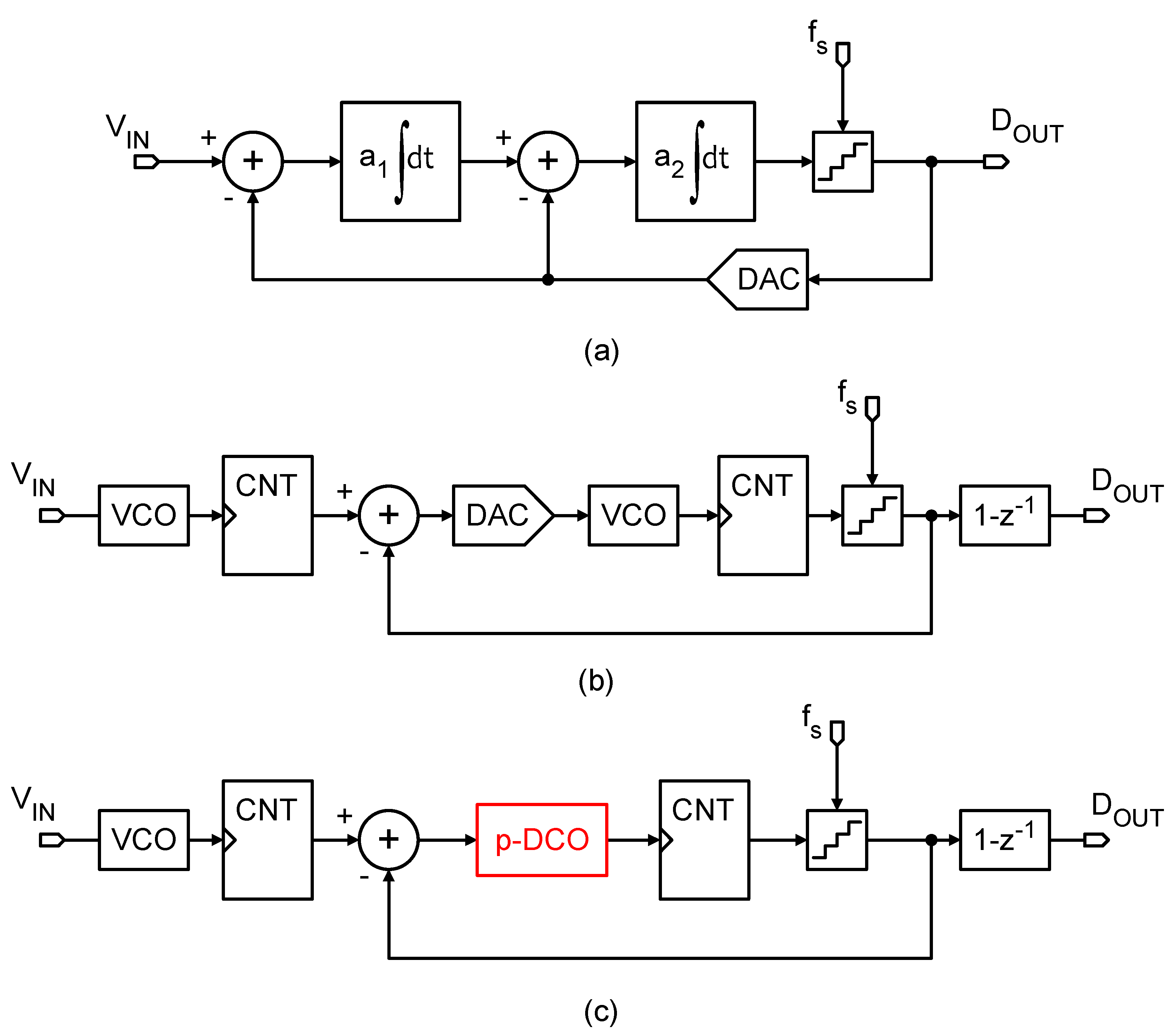
2. System-Level Description of the Proposed Architecture
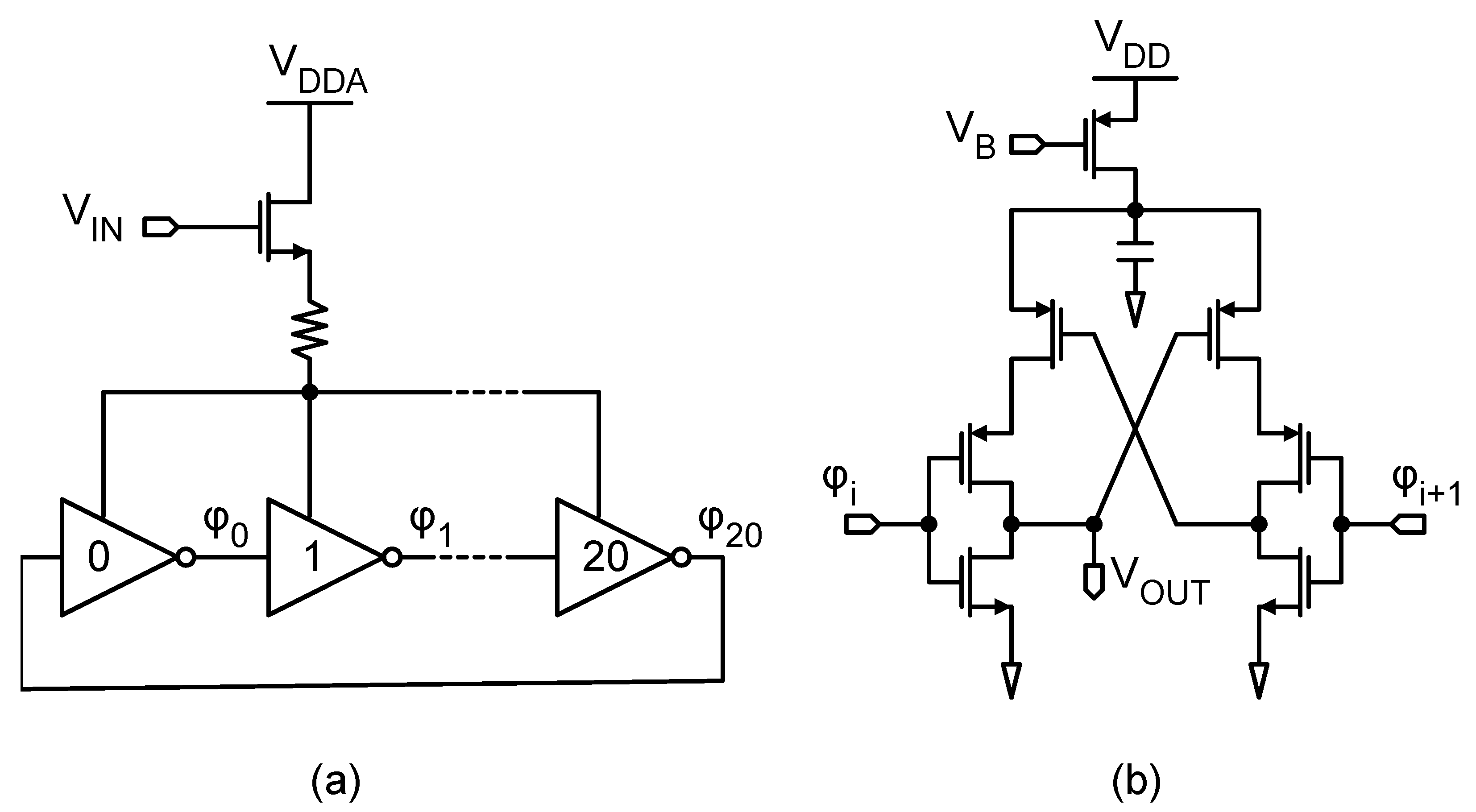
Direct digital synthesis (DDS) is widely used in many applications as a robust and scalable alternative to mixed-signal digitally controlled oscillators; however, it is not suitable for ultra-low power applications given its quite demanding power requirements. Therefore, we propose a novel topology called pseudo-DCO with the goal of addressing the drawbacks of DDS but maintaining the scalability and robustness to PVT variations.

2.1. Pseudo-DCO

The pseudo-DCO is based on combining orthogonal signals (eigenrates) generated by a master sequence generator. The sequences of this generator are combined linearly depending on a binary control input. The sequence generator can be shared by several instances of the pseudo-DCO in a SoC (system on a chip) hosting an array of ADCs, as schematically exemplified in Figure 3a. In [9], an early version of pseudo-DCO was described for the implementation of spiking-neural-network hardware accelerators; however, that implementation required delay-lines which are very sensitive to PVT variations and severely compromised the robustness of the system. Figure 2a shows the diagram of a 4-bit sequence generator. The width of the pulses depends on the duty-cycle of the driving clock f m . To avoid phase ambiguity, the frequency divider connected D-Flip-Flops must be reset at start-up, which is performed via an asynchronous initialization signal not shown in the figure.
The eigenrate generator produces 4 base sequences s b <3:0>, whose frequencies are f m divided by successive powers of two. In the chronograph of Figure 2b, it can be seen that the output pulses of the eigenrates do not overlap. Therefore, they can be combined by means of CMOS OR-gates. The digital-to-frequency conversion is performed selecting the corresponding eigenrates with an AND-gate according to the bits of the digital control word D I N . The selected eigenrates are combined in a single-bit signal with a multiple input OR-gate, as shown in Figure 3b. Equation (1) describes the frequency synthesis. On average, the frequency f d c o of the output signal s d c o is proportional to D I N . The frequency-to-input ratio (DCO gain) of the pseudo-DCO is given by f m / 2 4 , and its input–output characteristic is expressed in (2).
s d c o = i = 0 3 D I N < i > · s b < i >
f d c o = f m 16 i = 0 3 2 i · D I N < i >
Combining the eigenrates to generate an arbitrary output frequency inevitably produces a systematic phase error. Although the number of pulses per second will correspond to the desired frequency on average, the output waveform will not have equally spaced pulses. In order to mitigate the effect of such a phase error on the converter performance, it is possible to clock the sequence generator faster (overrunning) and subsequently divide the frequency by means of an asynchronous digital counter in order to maintain the gain of the DCO. This can be practically carried out by increasing the number of flip-flops in CNT1 and only taking the most significant 4 bits as the output. Let ORR represent the over-running ratio of the sequence generator. If we want a pseudo-DCO sensitivity of f s , the driving clock must be f m = 2 4 · ORR · f s in our case. This means we would need an additional log 2 ( ORR ) bits in CNT1 (assuming ORR is a power of 2) to properly adjust the frequency.
Figure 3. (a) Deployment of multiple pseudo-DCOs driven by one sequence generator. (b) A 4-bit pseudo-DCO implementation. (c) Second-order Δ Σ -ADC implementation.
Sensors 24 08029 g003

2.2. Input VCO and System-Level Simulations

The proposed second-order true-VCO Δ Σ -ADC, as shown in Figure 3c, was designed and simulated at both system and transistor levels using a 130 nm CMOS technology. The architecture features a 1 MHz sampling rate and utilizes a 4-bit data-path that includes both input and output counters. The design employs an input VCO implemented as a 21-tap ring oscillator, which is driven by an NMOS transconductor as illustrated in Figure 4a. The resistive degeneration at the source of the transconductor improves the linearity of the VCO, providing negative feedback at the inverters control node. The degeneration resistor was sized to 1 kΩ, and it was implemented as a polysilicon resistor 5 μm wide and 15 μm long. To accurately represent the digital state variables within the 4-bit data-path, the system was initially modeled behaviorally without noise and distortion. These simulations indicated that, for a full-scale input, the system could reach up to 11 output quantization levels without causing saturation of internal state variables, despite an expected maximum of 16 levels. This discrepancy has been previously explained in [8,10]. To maximize the dynamic range of the converter, the rest frequency of the input VCO must be set to 11 / 2 × 1 MHz. Assuming an analog supply V D D A = 1.2 V, this is achieved in our design with a DC biasing level of 900 mV at the gate of the input transconductor, yielding a rest frequency of 809 kHz. This frequency is multiplied up to 5.66 MHz by combining 7 phases of the VCO with XOR gates. These seven outputs are equipped with level shifters implemented as in Figure 4b to drive the XOR gates with compatible logic levels, while the rest of the output phases are loaded with dummy-level shifter replicas (see [8]). In the plot of Figure 5, we represent the peak signal-to-noise-and-distortion ratio (SNDR) as the ORR increases. Noticeably, as the performance of the pseudo-DCO asymptotically approaches the ideal-DCO, the asymptotic horizontal line is obtained, replacing the pseudo-DCO with a verilog-A ideal model. In the same figure, the peak SNDR of a first-order Δ Σ -modulator is also reported, and the second-order solution outperforms it for ORR > 3. The dependence of the SNDR on the ORR provides a straightforward mechanism to switch between different power modes. The ORR can be dynamically adjusted depending on the activity of the input signal. For example, in a voice recognition application, the device will most often be in an idle state, only functioning as an activity detector. In this situation, the ORR can drop down to 4, providing an SNDR of 52 dB; however, when the signal of interest is detected, the ORR may ramp up to 64, gaining an additional 16 dB in SNDR. This situation is common in other applications as well, such as biomedical signal acquisition chains.

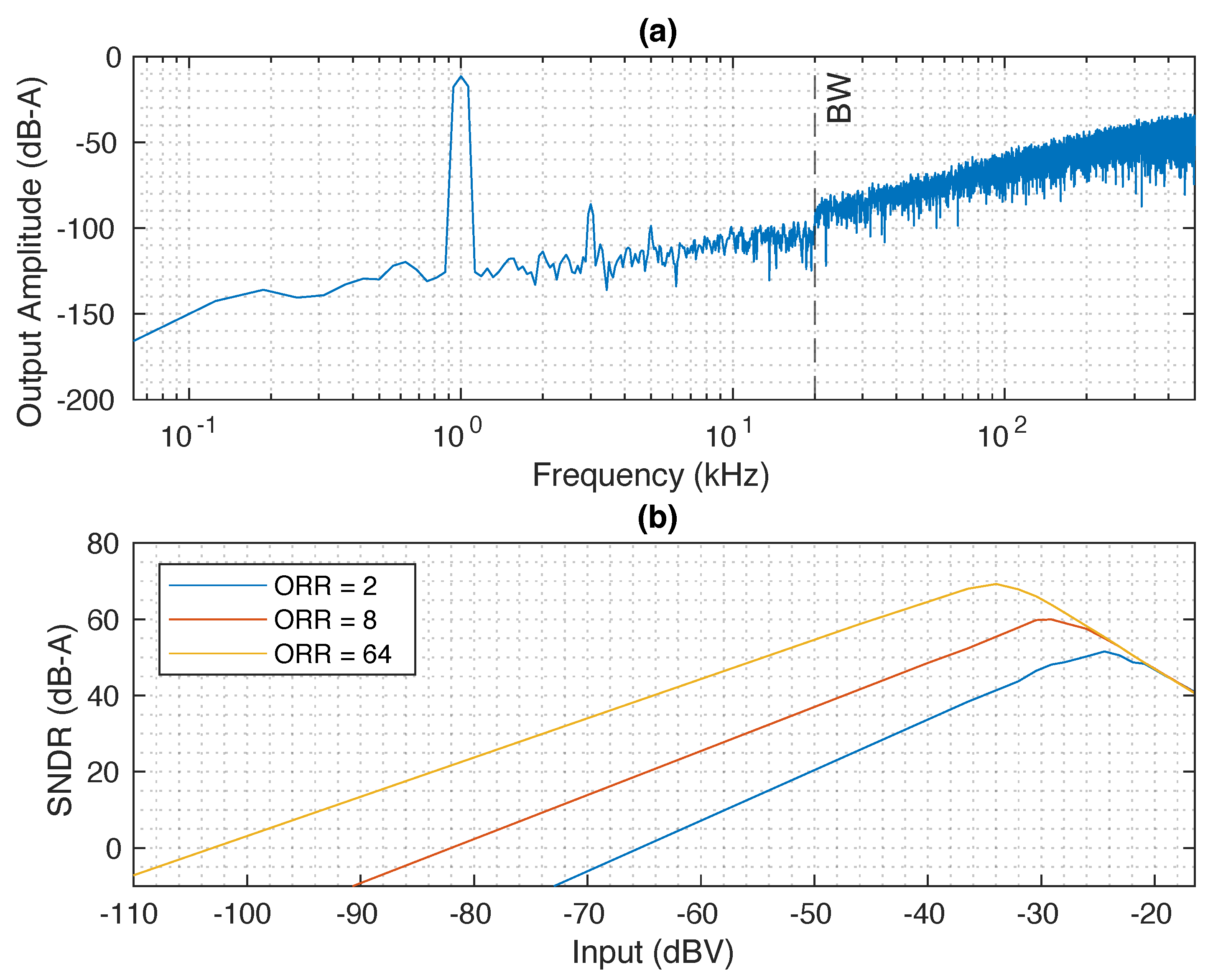
3. Post-Layout Results

The converter in a pseudo-differential configuration [2] was designed and validated with post-layout simulations in a 130 nm CMOS technology node. The ADC core takes 0.034 mm2 of a chip area, consuming a total power of 105.57 μW, with an ORR = 64 and a digital supply voltage of 0.9 V. To study the limits of the new frequency-to-digital converter stage, the transconductor and VCO were sized such that their thermal noise and distortion do not limit the SNDR of the converter. According to our calculations, in order to max out the capabilities of the input VCO, we would require a 5-bit data-path. However, the aim of this work is to study the limits of the novel architecture; therefore, we opted for the 4-bit solution. The peak SNDR is 69 dB, which was achieved with a voltage swing of 20 mV around the DC value. In Figure 5, we have annotated some points with the simulated post-layout power consumption of the whole chip to show the power scaling according to the ORR. In Figure 6a, we have represented the averaged output spectrum of the ADC with A-weighted filtering. The input tone is at 1 kHz with an amplitude of 20 mV, which is compatible with the voltage provided by a commercial MEMS microphone. Noticeably, the converter is not limited by the thermal noise floor of the input-VCO, as can be seen from the shaped in-band noise floor. The plot in Figure 6b shows the dynamic range of the converter for a selection of ORR values. All the simulations shown in Figure 6 are performed with a detailed post-layout model, including noise and distortion. Additionally, we did not see any performance degradation across corners, temperature and supply voltage sweeps. The layout of the proposed system is shown in Figure 7a, whilst Figure 7b depicts the power consumption breakdown, from which we can see that the majority of the power is consumed by the eigenrate generator. Table 1 shows a comparison of the proposed circuit with other recently published VCO-based ADCs. The proposed ADC shows the smallest area for the same signal bandwidth. Furthermore, figure of merit (FoM) estimations are in par with other designs. As a further advantage of our solution, the eigenrate generator can be shared among multiple pseudo-DCO instantiations scaling down its power share by the number of pseudo-DCOs in the SoC. This feature makes it particularly suitable for the implementation of ADC arrays. For example, an array of 16 ADCs would reduce the power share of the eigenrate generator per ADC channel to 3.75 μW, making it utterly impactless in the SoC power budget. If 16 ADCs are packed together, the SNDR FoM and DR FoM reported in Table 1 increase to 155 dB, and 176 dB, respectively. The power consumption of the input VCO is independent of the ORR, as it only effects the eigenrate generator and the digital electronics constituting the pseudo-DCO.

4. Conclusions

A novel digital-to-frequency converter, referred to as the pseudo-DCO, was proposed and thoroughly characterized. This pseudo-DCO was employed to implement the second stage of a second-order true-VCO Δ Σ modulator in a 130 nm CMOS process. The ADC exhibits excellent performance in post-layout simulations, achieving a peak SNDR of 69 dB and a dynamic range (DR) of 90 dB in maximum performance mode. The device’s performance and power consumption can be dynamically adjusted based on input activity, further improving the FoM. As a predominantly digital design, the converter is less sensitive to PVT variations compared to equivalent mixed-signal implementations, as confirmed by corner and Monte Carlo simulations. Furthermore, the pseudo-DCO scalability property makes it advantageous for multiple instantiations within a single SoC, making it particularly suitable for sensor arrays. Edge devices, where chip area and power consumption are critical constraints, will benefit the most from this proposed solution.

Author Contributions

Conceptualization, D.L. and L.H.C.; methodology, L.H.C.; software, D.L. and V.M.; validation, L.H.C.; formal analysis, D.L.; investigation, D.L.; resources, V.M. and L.H.C.; data curation, D.L.; writing—original draft preparation, D.L.; writing—review and editing, D.L. and L.H.C.; visualization, D.L., V.M. and L.H.C.; supervision, L.H.C.; project administration, L.H.C.; funding acquisition, L.H.C. All authors have read and agreed to the published version of the manuscript.

Funding

This work was supported by program H2020-MSCA-ITN-2020, grant No. 956601, and project PID2020-118804RB-I00 of AEI.

Institutional Review Board Statement

Not applicable.

Informed Consent Statement

Not applicable.

Data Availability Statement

Data are available upon request.

Conflicts of Interest

The authors declare no conflicts of interest.

Abbreviations

The following abbreviations are used in this manuscript:
VCOVoltage controlled oscillator
ADCAnalog-to-digital converter
ENOBEffective number of bits
PVTProcess, voltage and temperature
CMOSComplementary metal oxide semiconductor
SoCSystem on a chip
DCDirect current
PFMPulse frequency modulation
DACDigital-to-analog converter
DDSDirect digital synthesis
DCODigitally controlled oscillator
ORROverrunning ratio
SNDRSignal-to-noise-and-distortion ratio
MEMSMicro electro-mechanical system
FoMFigure of merit

References

  1. Gielen, G.G.; Hernandez, L.; Rombouts, P. Time-Encoding Analog-to-Digital Converters: Bridging the Analog Gap to Advanced Digital CMOS-Part 1: Basic Principles. IEEE Solid-State Circuits Mag. 2020, 12, 47–55. [Google Scholar] [CrossRef]
  2. Gielen, G.G.; Hernandez, L.; Rombouts, P. Time-Encoding Analog-to-Digital Converters: Bridging the Analog Gap to Advanced Digital CMOS-Part 2: Architectures and Circuits. IEEE Solid-State Circuits Mag. 2020, 12, 18–27. [Google Scholar] [CrossRef]
  3. Zhong, Y.; Sun, N. A Survey of Voltage-Controlled-Oscillator-Based ΔΣ ADCs. Tsinghua Sci. Technol. 2022, 27, 472–480. [Google Scholar] [CrossRef]
  4. Gutierrez, E.; Hernandez, L.; Cardes, F.; Rombouts, P. A Pulse Frequency Modulation Interpretation of VCOs Enabling VCO-ADC Architectures with Extended Noise Shaping. IEEE Trans. Circuits Syst. I: Regul. Pap. 2018, 65, 444–457. [Google Scholar] [CrossRef]
  5. Babaie-Fishani, A.; Rombouts, P. True High-Order VCO-based ADC. Electron. Lett. 2015, 51, 23–25. [Google Scholar] [CrossRef]
  6. Babaie-Fishani, A.; Rombouts, P. A Mostly Digital VCO-Based CT-SDM with Third-Order Noise Shaping. IEEE J. Solid-State Circuits 2017, 52, 2141–2153. [Google Scholar] [CrossRef]
  7. Cardes, F.; Gutierrez, E.; Quintero, A.; Buffa, C.; Wiesbauer, A.; Hernandez, L. 0.04-Mm2 103-dB-A Dynamic Range Second-Order VCO-Based Audio ΣΔ-ADC in 0.13-Mm CMOS. IEEE J. Solid-State Circuits 2018, 53, 1731–1742. [Google Scholar] [CrossRef]
  8. Medina, V.; Garvi, R.; Granizo, J.; Amaral, P.; Hernandez, L. A Second-Order Audio VCO-ADC with 103-dB-A Dynamic Range and Binary-Weighted Internal Architecture. arXiv 2024, arXiv:2405.07887. [Google Scholar]
  9. Loi, D.; Granizo, J.; Hernandez, L. A Scalable and PVT Invariant Spiking Neuron Using Asynchronous CMOS Logic. In Proceedings of the 2024 IEEE International Symposium on Circuits and Systems (ISCAS), Singapore, 19–22 May 2024; pp. 1–5. [Google Scholar] [CrossRef]
  10. Medina, V.; Rombouts, P.; Hernandez-Corporales, L. A Different View of Sigma-Delta Modulators Under the Lens of Pulse Frequency Modulation [Feature]. IEEE Circuits Syst. Mag. 2024, 24, 80–97. [Google Scholar] [CrossRef]
  11. Perez, C.; Garvi, R.; Lopez, G.; Quintero, A.; Leger, F.; Amaral, P.; Wiesbauer, A.; Hernandez, L. A VCO-Based ADC with Direct Connection to a Microphone MEMS, 80-dB Peak SNDR and 438-μW Power Consumption. IEEE Sens. J. 2023, 23, 8466–8477. [Google Scholar] [CrossRef]
  12. Zhang, M.; Spiegel, J.V.D.; Wang, Z. Low Power Circuit Design Using Advanced CMOS Technology, 1st ed.; River Publishers: Aalborg, Denmark, 2018. [Google Scholar] [CrossRef]
  13. Huang, J.; Mercier, P.P. A 94.2-dB SNDR 142.6-μW VCO-Based Audio ADC with a Split-ADC Differential Pulse Code Modulation Architecture. IEEE Solid-State Circuits Lett. 2021, 4, 121–124. [Google Scholar] [CrossRef]
  14. Zhao, X.; Li, D.; Zhang, X.; Liu, S.; Zhu, Z. A 0.6-V 94-nW 10-Bit 200-kS/s Single-Ended SAR ADC for Implantable Biosensor Applications. IEEE Sens. J. 2022, 22, 17904–17913. [Google Scholar] [CrossRef]
Figure 1. (a) Conventional second-order Δ Σ -ADC. (b) Equivalent true-VCO ADC requiring a loop DCO. (c) Proposed architecture employing a fully digital Pseudo-DCO.
Sensors 24 08029 g001
Figure 2. (a) Four bits sequence generator the FF must be properly initialize to guarantee the correct functionality of the circuit. (b) Relevant sequence generator signals showing the “orthogonality” of the sequences.
Sensors 24 08029 g002
Figure 4. (a) Schematic of the 21-tap input VCO. (b) Schematic of the level shifter loading the output phases of the VCO.
Sensors 24 08029 g004
Figure 5. Peak SNDR vs. ORR and post-layout power simulation. The dashed lines are the ideal-DCO and first-order ADC.
Sensors 24 08029 g005
Figure 6. (a) Output spectrum of the proposed system with an input of 20 mV. (b) Dynamic range of the proposed system, the DR and the peak SNDR scale with the ORR.
Sensors 24 08029 g006
Figure 7. (a) Layout of one branch of the proposed converter. (b) Power breakdown, with the following parameters: ORR = 64, f s = 1 MHz, f i n = 1 kHz, and A i n = 20 mV.
Sensors 24 08029 g007
Table 1. Comparison with other studies.
ReferenceThis Work[8][11][12][13][14]
Process130 nm130 nm130 nm28 nm65 nm65 nm
Supply (A/D) (V)1.2/0.91.5/0.951.5/0.951.1/0.551/10.6/0.6
BW (kHz)2020201020100
Area (mm2)0.0340.0950.140.0950.110.022
Power (uW)105.6250438.1170.5142.70.094
Sampling (MHz)13.0723.0722.420.2
DR (dB)9010310891100.3N.A.
FOM SNDR (dB)153155.5157152.6175.5176.6
FOM DR (dB)173182184.6170.4181.8N.A.
Disclaimer/Publisher’s Note: The statements, opinions and data contained in all publications are solely those of the individual author(s) and contributor(s) and not of MDPI and/or the editor(s). MDPI and/or the editor(s) disclaim responsibility for any injury to people or property resulting from any ideas, methods, instructions or products referred to in the content.

