

A Circularly Polarized Non-Resonant Slotted Waveguide Antenna Array for Wide-Angle Scanning


Abstract
1. Introduction
- A center-set waveguide slot element on the centerline of the broad wall is proposed to set up a waveguide circular polarizer with four ridges;
- A compact circular polarized slotted waveguide planar array is presented that can realize a wide phase scanning range.
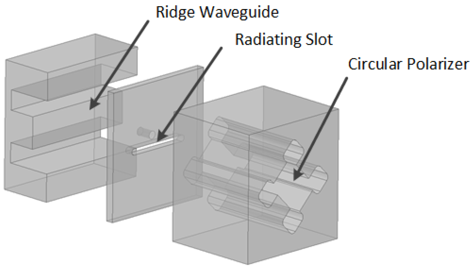
2. Configuration of the Antenna Element
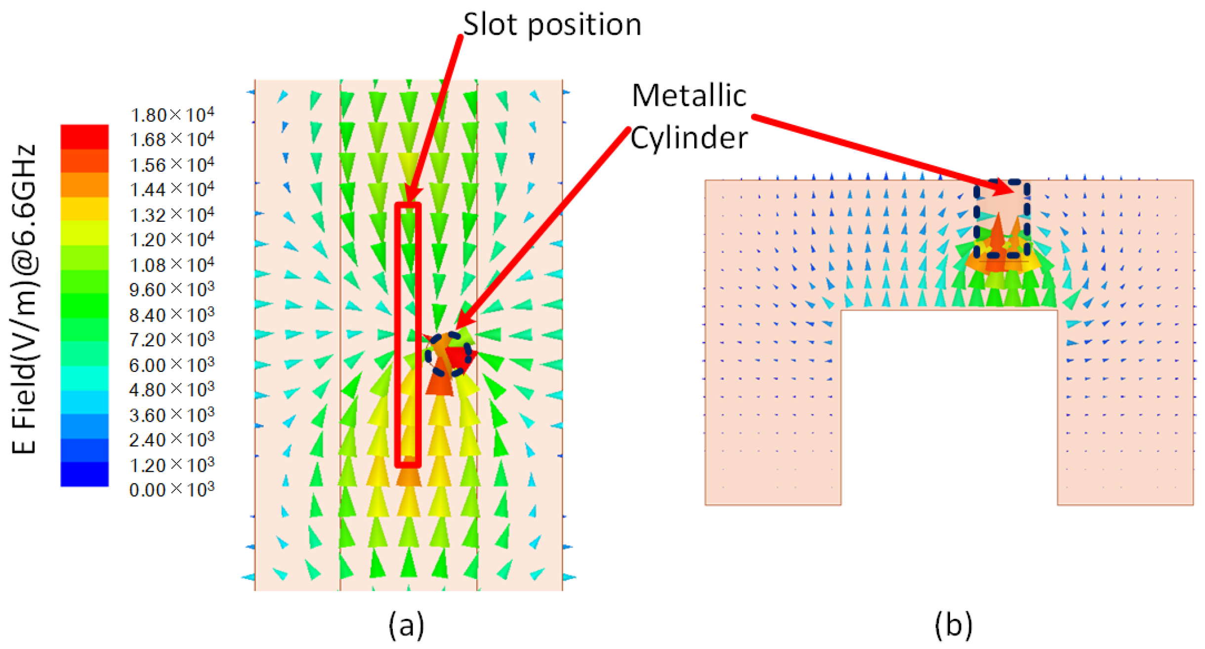
2.1. Design of Circular Polarizer
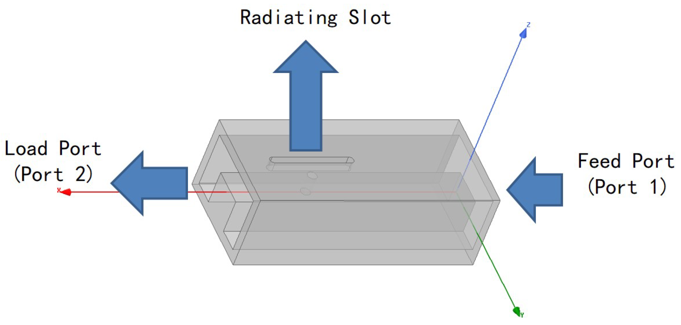
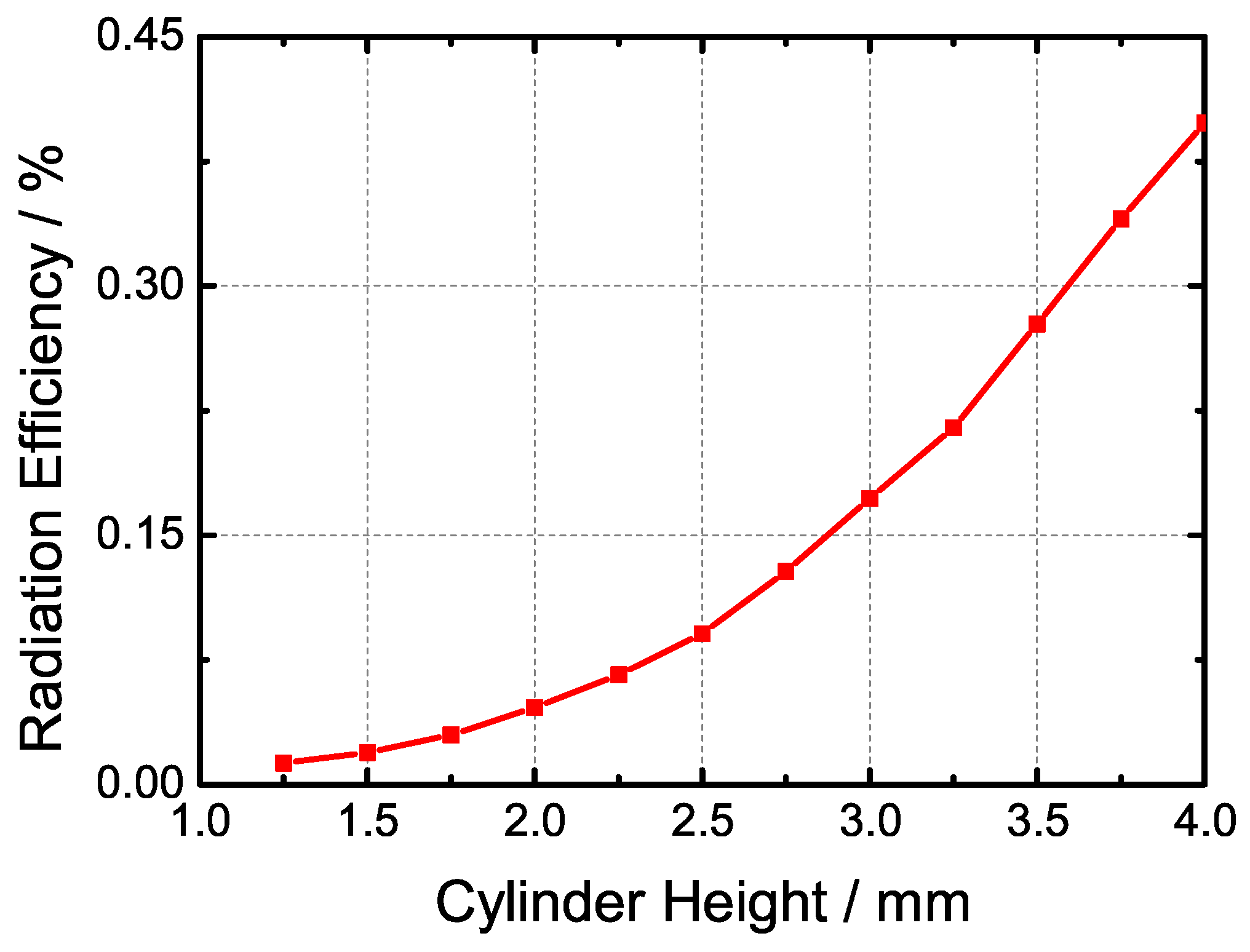
2.2. Slotted Waveguide with Metallic Cylinder Inside
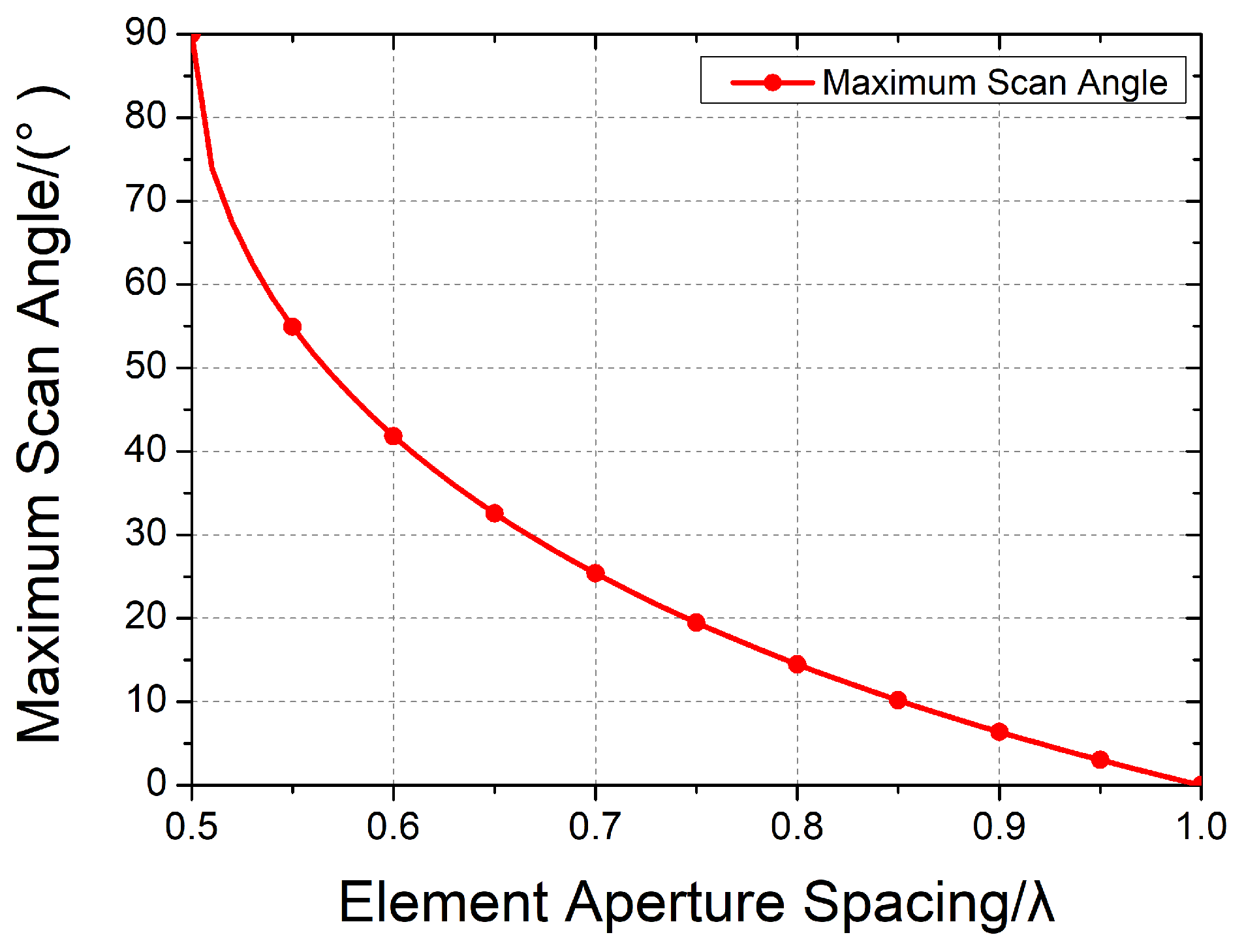
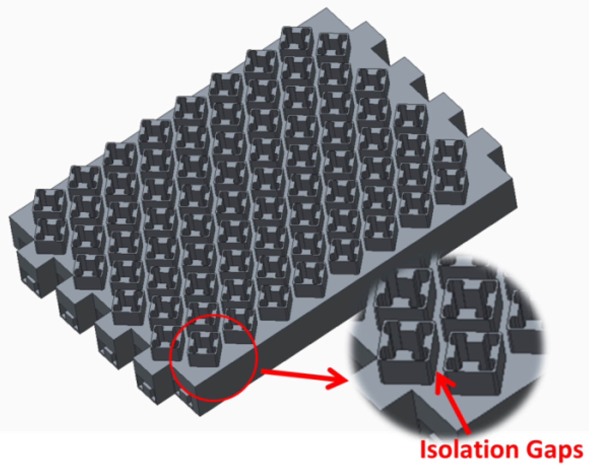
3. Design of Antenna Array
3.1. Linear Array
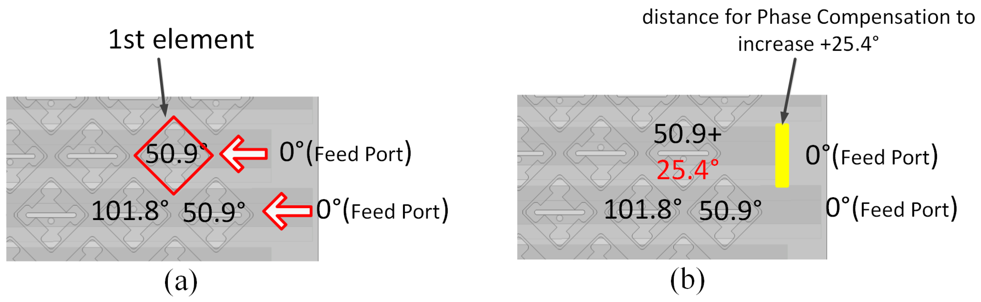
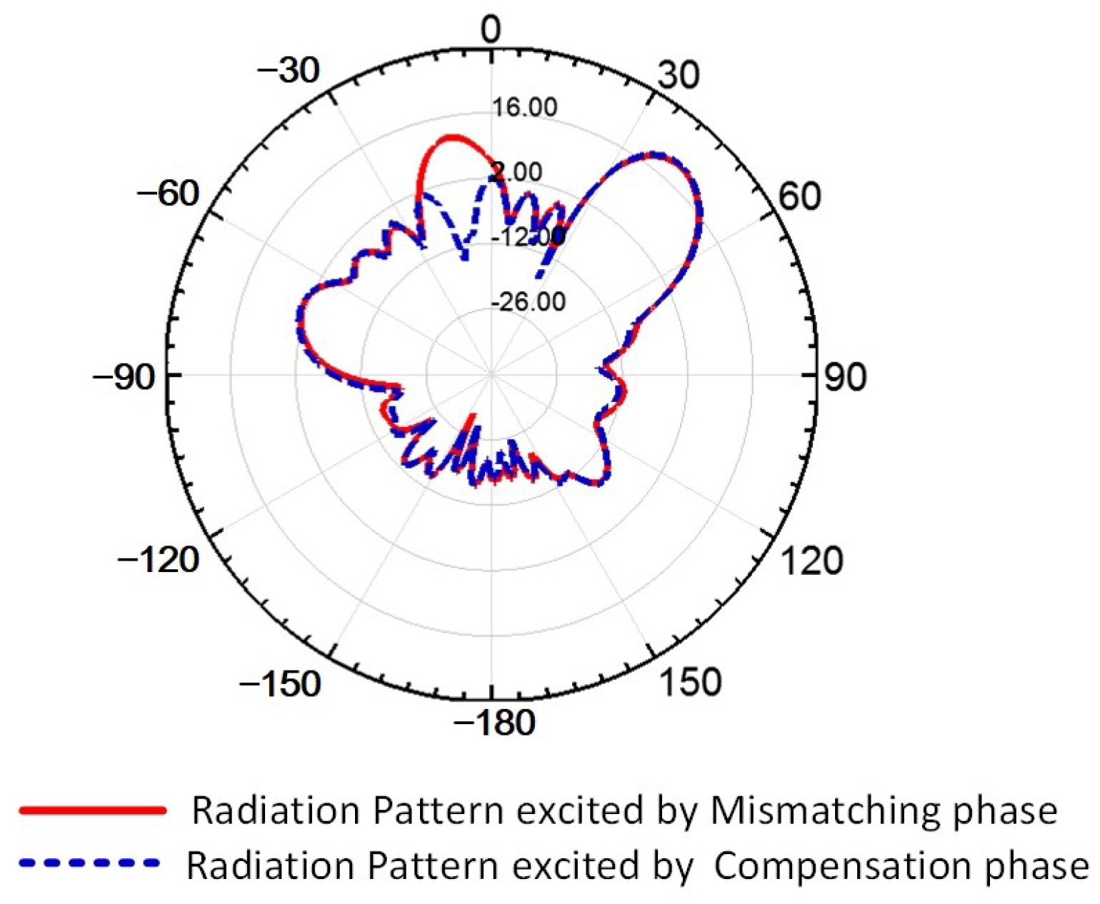
3.2. Planar Array
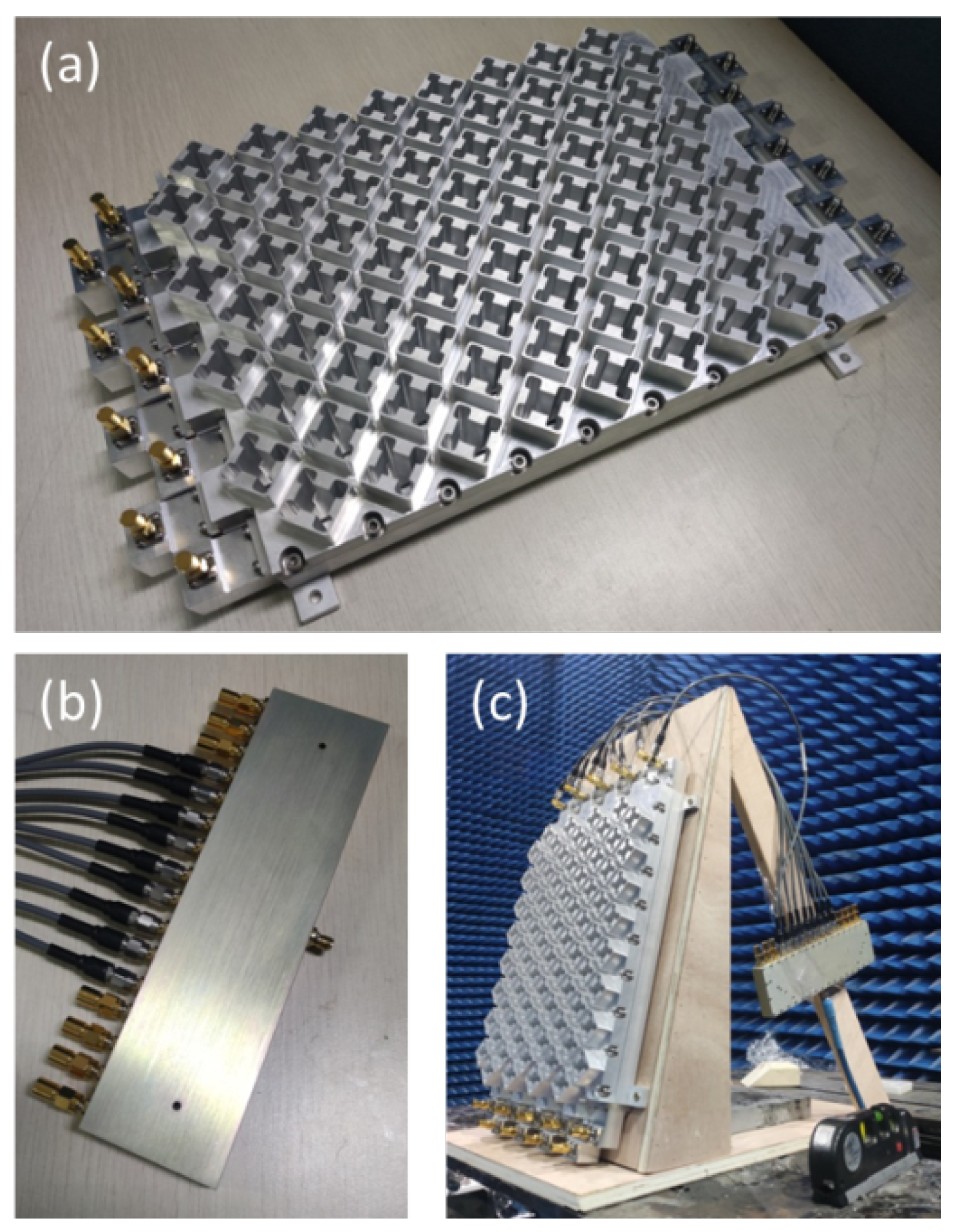
4. Verification and Comparison
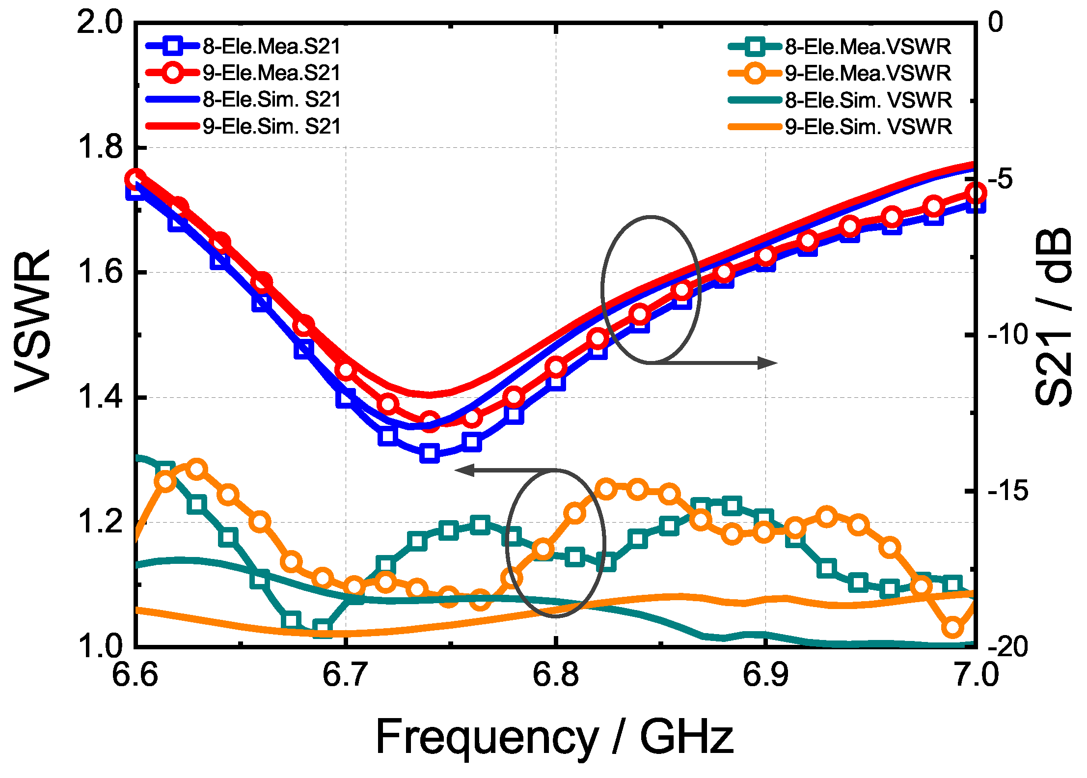
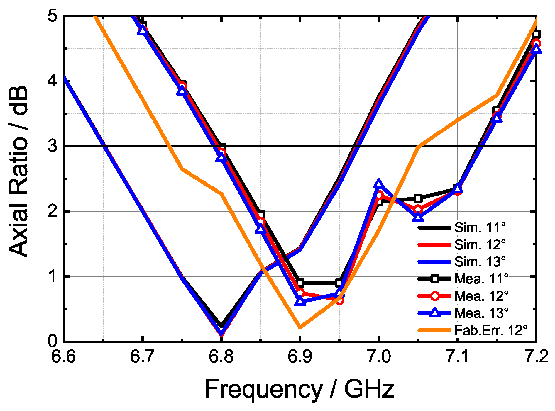
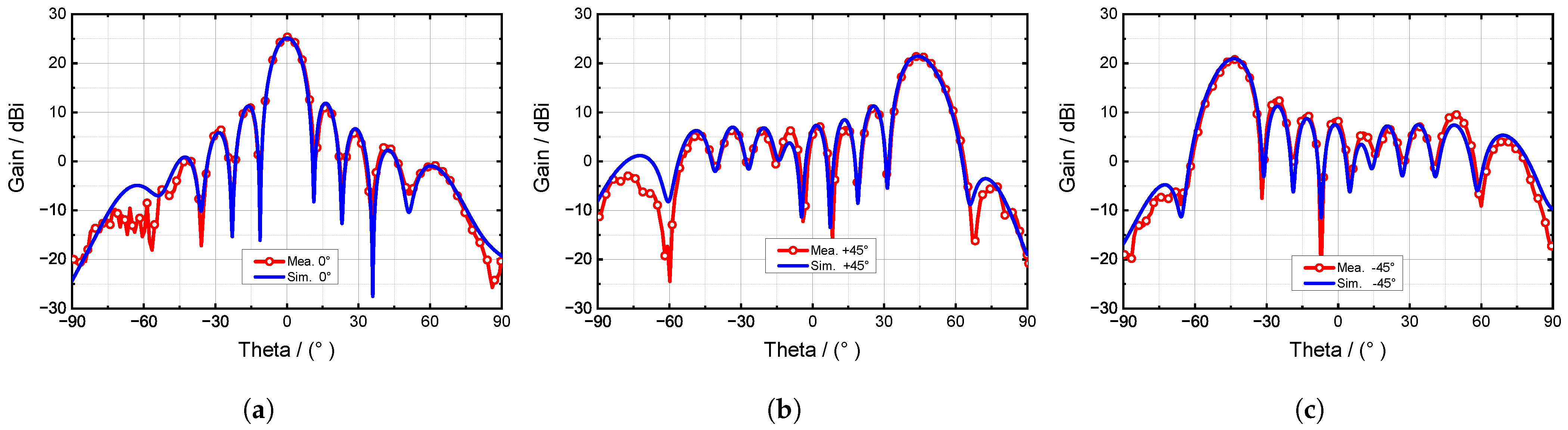
4.1. Simulation and Measurement Results
4.2. Comparison and Discussion
5. Conclusions
Author Contributions
Funding
Institutional Review Board Statement
Informed Consent Statement
Data Availability Statement
Conflicts of Interest
References
- Troughton, J.; Evans, B. Rain-induced deflection of microwave and millimetre-wave radiowaves. Electron. Lett. 1976, 12, 68–70. [Google Scholar] [CrossRef]
- Yang, R.; Wu, Z.; Chen, Y. Study of electromagnetic wave scattering and attenuation properties due to a melting layer of precipitation. J. Xidian Univ. 2002, 29, 451–454. [Google Scholar]
- Aljuhani, A.H.; Kanar, T.; Zihir, S.; Rebeiz, G.M. A 256-element Ku-band polarization agile SATCOM receive phased array with wide-angle scanning and high polarization purity. IEEE Trans. Microw. Theory Tech. 2021, 69, 2609–2628. [Google Scholar] [CrossRef]
- Han, G.; Du, B.; Wu, W.; Yang, B. A novel hybrid phased array antenna for satellite communication on-the-move in Ku-band. IEEE Trans. Antennas Propag. 2015, 63, 1375–1383. [Google Scholar] [CrossRef]
- Yang, H.; Montisci, G.; Jin, Z.; Liu, Y.; He, X.; Mazzarella, G. Improved design of low sidelobe substrate integrated waveguide longitudinal slot array. IEEE Antennas Wirel. Propag. Lett. 2014, 14, 237–240. [Google Scholar] [CrossRef]
- Le Sage, G.P. 3D printed waveguide slot array antennas. IEEE Access 2016, 4, 1258–1265. [Google Scholar] [CrossRef]
- Aboserwal, N.; Salazar-Cerreno, J.L.; Qamar, Z. An ultra-compact X-band dual-polarized slotted waveguide array unit cell for large E-scanning radar systems. IEEE Access 2020, 8, 210651–210662. [Google Scholar] [CrossRef]
- Ren, Y.; Li, K.; Wang, F.; Wu, H.; Zhang, Y.; Li, L. A Dual-Polarized Phased-Array Antenna Based on Single Ridge Slotted Waveguide Array. In Proceedings of the 2019 Cross Strait Quad-Regional Radio Science and Wireless Technology Conference (CSQRWC), Taiyuan, China, 8–21 July 2019; pp. 1–3. [Google Scholar]
- Chen, X.Q.; Wu, Q.; Tian, M.X. Study on the return loss characteristics of rectangular single ridge waveguide slot. In Proceedings of the 2013 IEEE International Conference on Applied Superconductivity and Electromagnetic Devices, Beijing, China, 25–27 October 2013; pp. 468–472. [Google Scholar]
- Stoumpos, C.; Le Gouguec, T.; Allanic, R.; García-Vigueras, M.; Amiaud, A.C. Compact additively manufactured conformal slotted waveguide antenna array. IEEE Antennas Wirel. Propag. Lett. 2023, 28, 1843–1847. [Google Scholar] [CrossRef]
- Chen, Q.; Yan, S.; Guo, X.; Qu, C.; Liu, J.; Huang, Z.; Yang, L.; Li, Y.; Liang, X. A 77 GHz Phased Array Antenna Based on Substrate Integrated Waveguide. IEEE Antennas Wirel. Propag. Lett. 2023, 22, 2979–2983. [Google Scholar] [CrossRef]
- He, J.; Wu, Y.; Chen, D.; Zhang, M.; Hirokawa, J.; Liu, Q. Realization of a wideband series-fed 4× 4-element waveguide slot array in the X-band. IEEE Access 2021, 9, 83666–83675. [Google Scholar] [CrossRef]
- Luo, H.; Xiao, Y.; Lu, X.; Sun, H. Design of a dual-polarization single-ridged waveguide slot array with enhanced bandwidth. IEEE Antennas Wirel. Propag. Lett. 2018, 18, 138–142. [Google Scholar] [CrossRef]
- Chen, M.; Fang, X.C.; Wang, W.; Zhang, H.T.; Huang, G.L. Dual-band dual-polarized waveguide slot antenna for SAR applications. IEEE Antennas Wirel. Propag. Lett. 2020, 19, 1719–1723. [Google Scholar] [CrossRef]
- Lu, J.; Zhang, H.; Wang, W.; Liang, X.; Ge, J.; Jin, M.; Wu, W. Broadband dual-polarized waveguide slot filtenna array with low cross polarization and high efficiency. IEEE Trans. Antennas Propag. 2018, 67, 151–159. [Google Scholar] [CrossRef]
- Chen, P.; Hong, W.; Kuai, Z.; Xu, J. A substrate integrated waveguide circular polarized slot radiator and its linear array. IEEE Antennas Wirel. Propag. Lett. 2008, 8, 120–123. [Google Scholar] [CrossRef]
- Montisci, G. Design of circularly polarized waveguide slot linear arrays. IEEE Trans. Antennas Propag. 2006, 54, 3025–3029. [Google Scholar] [CrossRef]
- Dimitrov, K.C.; Lee, Y.; Min, B.W.; Park, J.; Jeong, J.; Kim, H.J. Circularly polarized T-shaped slot waveguide array antenna for satellite communications. IEEE Antennas Wirel. Propag. Lett. 2019, 19, 317–321. [Google Scholar] [CrossRef]
- Kazemi, R.; Yang, S.; Suleiman, S.H.; Fathy, A.E. Design procedure for compact dual-circularly polarized slotted substrate integrated waveguide antenna arrays. IEEE Trans. Antennas Propag. 2019, 67, 3839–3852. [Google Scholar] [CrossRef]
- Al Sharkawy, M.; Kishk, A.A. Wideband beam-scanning circularly polarized inclined slots using ridge gap waveguide. IEEE Antennas Wirel. Propag. Lett. 2014, 13, 1187–1190. [Google Scholar] [CrossRef]
- Xu, J.; Wang, M.; Huang, H.; Wu, W. Circularly polarized patch array fed by slotted waveguide. IEEE Antennas Wirel. Propag. Lett. 2014, 14, 8–11. [Google Scholar] [CrossRef]
- Ferrando-Rocher, M.; Herranz-Herruzo, J.I.; Valero-Nogueira, A.; Rodrigo, V.M. Circularly polarized slotted waveguide array with improved axial ratio performance. IEEE Trans. Antennas Propag. 2016, 64, 4144–4148. [Google Scholar] [CrossRef]
- Tomura, T.; Saito, Y.; Hirokawa, J. 8× 2-element 60-GHz-band circularly polarized post-wall waveguide slot array antenna loaded with dipoles. IEEE Access 2020, 8, 85950–85957. [Google Scholar] [CrossRef]
- Cao, J.; Wang, H.; Mou, S.; Soothar, P.; Zhou, J. An air cavity-fed circularly polarized magneto-electric dipole antenna array with gap waveguide technology for mm-wave applications. IEEE Trans. Antennas Propag. 2019, 67, 6211–6216. [Google Scholar] [CrossRef]
- Hoseini, M.; Forooraghi, K.; Abdolali, A. A Waveguide Slot-Fed Patch Antenna Array. IEEE Antennas Wirel. Propag. Lett. 2023, 22, 2027–2031. [Google Scholar] [CrossRef]
- Dogan, D.; Top, C.B. Circularly polarized Ka-band waveguide slot array with low sidelobes. In Proceedings of the 2012 6th European Conference on Antennas and Propagation (EUCAP), Prague, Czech Republic, 26–30 March 2012; pp. 1105–1109. [Google Scholar]
- Zarifi, D.; Farahbakhsh, A.; Zaman, A.U. A Dual-Circularly Polarized Gap Waveguide-Based Linear Array Antenna for 60 GHz-Band. In Proceedings of the 2023 17th European Conference on Antennas and Propagation (EuCAP), Florence, Italy, 26–31 March 2023; pp. 1–3. [Google Scholar]
- Chen, Q.; Wu, T.; Wan, Y.; Li, L.; Jin, M. A circularly polarized waveguide slot antenna for random array application. In Proceedings of the 2019 International Conference on Microwave and Millimeter Wave Technology (ICMMT), Guangzhou, China, 19–22 May 2019; pp. 1–3. [Google Scholar]
- Wu, X.; Yang, F.; Xu, F.; Zhou, J. Circularly polarized waveguide antenna with dual pairs of radiation slots at Ka-band. IEEE Antennas Wirel. Propag. Lett. 2017, 16, 2947–2950. [Google Scholar] [CrossRef]
- Li, Y.Q.; Zhang, H.; Fu, Y.Q.; Yuan, N.C. RCS reduction of ridged waveguide slot antenna array using EBG radar absorbing material. IEEE Antennas Wirel. Propag. Lett. 2008, 7, 473–476. [Google Scholar]
- Qiu, L.; Xiao, K.; Chai, S.L.; Qi, H.Y.; Mao, J.J. A double-layer shaped-beam traveling-wave slot array based on SIW. IEEE Trans. Antennas Propag. 2016, 64, 4639–4647. [Google Scholar] [CrossRef]
- Yin, W.; Chen, A.; Liang, X.; Shi, L.; Guan, F.; Liu, X.; Zi, J. Frequency scanning single-ridge serpentine dual-slot-waveguide array antenna. IEEE Access 2020, 8, 77245–77254. [Google Scholar] [CrossRef]
- Yuan, W.; Liang, X.; Zhang, L.; Geng, J.; Zhu, W.; Jin, R. Rectangular grating waveguide slot array antenna for SATCOM applications. IEEE Trans. Antennas Propag. 2019, 67, 3869–3880. [Google Scholar] [CrossRef]
- Moradian, M.; Tayarani, M.; Khalaj-Amirhosseini, M. Planar slotted array antenna fed by single wiggly-ridge waveguide. IEEE Antennas Wirel. Propag. Lett. 2011, 10, 764–767. [Google Scholar] [CrossRef]
- Jasik, H.; Mao, Y.; Lin, C. The Handbook of Antenna Engineering; National Defense Industry Press: Beijing, China, 1966; pp. 243–249. [Google Scholar]
- Jiang, Z. Antenna Princples; Beihang University Press: Beijing, China, 1993; pp. 195–199. [Google Scholar]


| Parameters | s1 | s2 | d1 | d2 | h |
|---|---|---|---|---|---|
| Value (mm) | 7.5 | 7.5 | 2.9 | 5.3 | 31.3 |
| Slot No. | Eight-Element Array’s Cylinder Height | Eight-Element Array’s Slot Length | Nine-Element Array’s Cylinder Height | Nine-Element Array’s Slot Length |
|---|---|---|---|---|
| 1 | 1.7 | 21.6 | 1.6 | 21.6 |
| 2 | 2.2 | 21.4 | 1.9 | 21.4 |
| 3 | 2.8 | 21.4 | 2.5 | 21.4 |
| 4 | 3.3 | 21.4 | 3.1 | 21.4 |
| 5 | 3.9 | 21.1 | 3.4 | 21.1 |
| 6 | 4.1 | 20.9 | 3.9 | 20.9 |
| 7 | 3.8 | 20.9 | 4.0 | 20.9 |
| 8 | 3.2 | 21.1 | 3.5 | 21.1 |
| 9 | N/A | N/A | 3.1 | 21.4 |
| Frequency/GHz | AR at 11°/dB | AR at 12°/dB | AR at 13°/dB |
|---|---|---|---|
| 6.7 | 2.01 | 2.01 | 2.00 |
| 6.8 | 0.24 | 0.10 | 0.12 |
| 6.9 | 1.44 | 1.43 | 1.41 |
| 7.0 | 3.76 | 3.71 | 3.64 |
| Scan Angle | −45° | 0° | +45° |
|---|---|---|---|
| Axial Ratio (Sim.) | 3.33 dB | 0.23 dB | 2.69 dB |
| Axial Ratio (Mea.) | 2.3 dB | 2.9 dB | 2.2 dB |
| Ref. | Feed Type | Polarizer Type | Number of Elements | Excitation Wave Type | Frequency Band (%) | El. Plane SLL (dB) | Gain (dBi) | Axial Ratio Band (%) | Scan Type | Scan Angle (°) |
|---|---|---|---|---|---|---|---|---|---|---|
| [17] | Waveguide | Slots | 1 × 15 | Traveling | 1.33 | −18 (Sim.) | 21 (Sim.) | >2.7 (Sim.) | - | - |
| [19] | SIW | Slots | 64 × 12 | Traveling | 8.03 | −14 | 28 | - | Freq | +36∼+49 (El.) |
| [20] | RGW | Slots | 1 × 7 | Traveling | 21.43 | - | 12.5 | 21 | Freq | −15∼+15 (El.) |
| [21] | Waveguide | Patches | 1 × 10 | Standing | 2.85 | −13 | 15.94 | 3.2 | - | - |
| [22] | Waveguide | Dipoles | 12 × 12 | Standing | 7.33 | −12 | 28.01 | 14 (Sim.) | - | - |
| [28] | Waveguide | Waveguide | 2 × 8 | Standing | 1.63 | −13 (Sim.) | 17 (Sim.) | - | Phase | -18∼+18 (Az.) |
| This work | Waveguide | Waveguide | 5 × 8 4 × 9 | Traveling | 5.89 | <−20 | 24.3 | 5.0 | Freq and Phase | +11∼+13 (El.) −45∼+45 (Az.) |
Disclaimer/Publisher’s Note: The statements, opinions and data contained in all publications are solely those of the individual author(s) and contributor(s) and not of MDPI and/or the editor(s). MDPI and/or the editor(s) disclaim responsibility for any injury to people or property resulting from any ideas, methods, instructions or products referred to in the content. |
© 2024 by the authors. Licensee MDPI, Basel, Switzerland. This article is an open access article distributed under the terms and conditions of the Creative Commons Attribution (CC BY) license (https://creativecommons.org/licenses/by/4.0/).
Share and Cite
Han, G.; Liu, W. A Circularly Polarized Non-Resonant Slotted Waveguide Antenna Array for Wide-Angle Scanning. Sensors 2024, 24, 3056. https://doi.org/10.3390/s24103056
Han G, Liu W. A Circularly Polarized Non-Resonant Slotted Waveguide Antenna Array for Wide-Angle Scanning. Sensors. 2024; 24(10):3056. https://doi.org/10.3390/s24103056
Chicago/Turabian StyleHan, Guodong, and Weihang Liu. 2024. "A Circularly Polarized Non-Resonant Slotted Waveguide Antenna Array for Wide-Angle Scanning" Sensors 24, no. 10: 3056. https://doi.org/10.3390/s24103056
APA StyleHan, G., & Liu, W. (2024). A Circularly Polarized Non-Resonant Slotted Waveguide Antenna Array for Wide-Angle Scanning. Sensors, 24(10), 3056. https://doi.org/10.3390/s24103056