Article

The Estimated Temperature of the Semiconductor Diode Junction on the Basis of the Remote Thermographic Measurement

by
Arkadiusz Hulewicz
1,*,
Krzysztof Dziarski
2 and
Zbigniew Krawiecki
1
1
Institute of Electrical Engineering and Electronics, Poznan University of Technology, Piotrowo 3A, 60-965 Poznan, Poland
2
Institute of Electric Power Engineering, Poznan University of Technology, Piotrowo 3A, 60-965 Poznan, Poland
*
Author to whom correspondence should be addressed.
Sensors 2023, 23(4), 1944; https://doi.org/10.3390/s23041944
Submission received: 28 November 2022 / Revised: 28 January 2023 / Accepted: 6 February 2023 / Published: 9 February 2023
(This article belongs to the Special Issue Next-Generation Temperature Sensors)

Abstract

:
The value of a semiconductor’s diode temperature determines the correct operation of this element and its useful lifetime. One of the methods for determining the die temperature of a semiconductor diode is through the use of indirect thermographic measurements. The accuracy of the thermographic temperature measurement of the diode case depends on the prevailing conditions. The temperature of the mold body (the black part of the diode case made of epoxy resin) depends on the place of measurement. The temperature of the place above the die is closer to the die temperature than the temperature of mold body fragments above the base plate. In addition, the difficulty of its thermographic temperature measurement increases when the surface whose temperature is being measured is in motion. Then, the temperature measured by thermography may not apply to the warmest point in the case where the die temperature is determined. Information about the difference between temperatures of the different parts of the mold body and the die may be important. For this reason, it was decided to check how much the temperature measurement error of the die diode changes if the temperature of the diode case is not measured at the point that is above the die.

1. Introduction

Some components mounted on printed circuit boards (PCBs) are semiconductor components. Semiconductor components are diodes and transistors. The correct operation of other elements placed on the PCB and, consequently, of the entire device depends on its proper operation [1]. Examples of devices in which semiconductor elements are used are AC/DC and DC/AC converters used in electromobility and renewable energy. Another example is devices that work as nodes on the Internet of Things (IoT) [2].
A semiconductor diode is an example of a semiconductor component. It is a single junction between two p-enriched (positive) and n-depleted (negative) regions. The p–n junction is placed in an epoxy mold compound. One area is connected to the lead frame with a fine wire less than 1 mm thick [3]. In the case of the TO-220 enclosure, the second area is connected to the metal back metal case. In turn, this part of the case is connected to the lead frame [4].
A semiconductor diode is a single junction between p-type and n-type semiconductors (mostly silicon) [3,4]. The correct operation of a semiconductor diode depends on the temperature of the semiconductor junction Tj. When the value of Tj is higher than the maximum value of Tjmax, the semiconductor junction will be damaged. The operation of the diode with an excessive value of Tj (Tj < Tjmaxc) shortens the life of the diode. Another effect of the operation of the semiconductor diode junction with Tj different from the value taken into account during the design process is a change in the characteristics that link the value of forward voltage VF and forward current IF (IF = f(VF)) [5]. It changes compared to the characteristics taken into account during the design process. As a consequence, a change in the Tj value changes the VF and IF values of the semiconductor junction [6].
Obtaining a stable semiconductor junction temperature is possible after using a cooling system. This is associated with additional costs. Oversized cooling systems increase the costs of cooling the semiconductor junction. However, when the selected cooling system dissipates heat incorrectly, the Tj value increases to excessively high values. Therefore, to verify the correct selection of the cooling system (e.g., heat sink), the value of Tj should be known [7].
There are several groups of methods that allow for estimation the Tj value. Direct methods belong to the first group of methods. The second group of methods is indirect methods. Direct methods can be divided into contact methods and noncontact methods. Indirect methods can be divided into contact, noncontact and electrical methods.
Direct methods include those that require access to the semiconductor junction. Direct contact methods rely on the application of a temperature sensor directly to a semiconductor junction. Noncontact direct methods rely on estimating the temperature of a semiconductor junction on the basis of optical radiation emitted by the junction [8]. It is also possible to estimate the junction temperature on the basis of the angle of reflection of the optical radiation from the semiconductor element [9].
The disadvantage of these methods is their necessity to destroy the case. It is an irreversible process. As a result of case destruction, the heat exchange between the junction and the environment changes. The distribution of thermal resistances on the junction–ambient path changes. For this reason, the temperature of the junction operating in the open case and the junction operating in the closed case is different. This is noticeable even when the same power Pj is dissipated at the junction.
The indirect methods do not require direct access to the semiconductor junction. They rely on estimating the temperature of the semiconductor junction on the basis of the temperature of the case. The temperature of the case can be measured with an applied temperature sensor. The disadvantage of this method is the unknown value of the thermal resistance between the junction and the case [10]. Applying the sensor to the case can change the temperature distribution on its surface. Another disadvantage of this method is the risk of applying a metal temperature sensor to the metal part of the case which may, consequently, result in an electric shock [11,12].
Electrical methods rely on determining the temperature of a semiconductor junction on the basis of a known value of an electrical parameter, the value of which depends on the temperature of the junction. The parameter is called the TSP (thermal sensitive parameter). For a semiconductor diode, TSP is VF. In order to determine the semiconductor junction temperature using this method, the characteristic Tj = f(TSP) must be known. It is not possible to determine identical characteristics for different junctions [13]. This is because of the impossibility of growing two identical semiconductor crystals. Furthermore, to determine the characteristic Tj = f(TSP), additional research should be performed. For this reason, the use of this method is awkward [14].
These inconveniences can be prevented by using thermography. This noncontact method allows for measuring the junction temperature on the basis of the power of IR radiation (InfraRed) reaching the IR radiation detectors [15]. With the radiation emitted by the observed case, the lens of the IR camera is reached by the radiation from neighboring objects and radiation emitted by the air layer located between the lens and the case of the electronic component. For this reason, during the thermographic measurement of the temperature of the case, the conditions that prevail during the measurement should be taken into account.
The most important of them include the value of the emissivity coefficient ε [16], the reflected temperature Tr [17], the distance between the lens and the observed object d [18], the ambient temperature Ta [19], the temperature of the external optical system [20], the transmittance of the external optical system [21,22], the relative humidity ω [23], the viewing angle β [24] and the sharpness of the recorded thermogram [25].
The case of semiconductor elements is made of various materials. Regarding TO cases (e.g., TO-247), the case consists of a copper plate on which a die is placed. The die is connected to the leads by bond wire and copper plate. The die is embedded in a mold body that is made of an EMC (epoxy molding compound). Case fragments have different values of ε. The back part of the case, which is made of bleached copper plate, has a lower ε value compared to the mold body. The closest to the die is the copper plate and the part of the mold body that is placed directly above the die. Metals have a high reflectance ρ. For this reason, the lens of the thermographic camera, in addition to the temperature of the copper plate, receives a large amount of IR radiation, which comes from neighboring objects. This feature makes thermographic measurements difficult in this spot.
The semiconductor elements are made of various materials. One of them is silicon carbide (SiC). Compared to silicon Si, SiC has a higher Tjmax value. Elements made on the basis of SiC are used in the areas of renewable energy and electromobility. For this reason, it was decided to carry out research work aimed at determining the junction temperature of a semiconductor diode made on the basis of SiC.
At the prototyping stage, the value of the junction temperature of the diode placed on the heat sink is important. This allows for the assessment of the operating point of the element and the correctness of heat sink selections. As a consequence, it is possible to minimize costs. The prototyping time is also important. The cases of the electronic components whose temperature is determined are usually small in size. Therefore, a precise measurement of the case temperature with a thermographic camera is required, which results in extending the useful life of the case.
Information about the differences between the temperature of the part of the mold body, which are above the die and the temperature of the part of the mold body, which are above the base plate, are unknown to the authors of this article. Articles about these differences are unknown to the authors, too. This information is difficult to find in the literature.
For this reason, it was decided to use the methods that would allow the remote execution of such a thermogram, on the basis of which it would be possible to estimate the junction temperature for a semiconductor diode. It was decided to check how the complexity of the applied algorithm affects the time of determining the die temperature. How much the die temperature determined on the basis of the maximum case temperature differs from the die temperature determined on the basis of the case temperature of another part of the mold body was also checked.

2. Materials and Methods

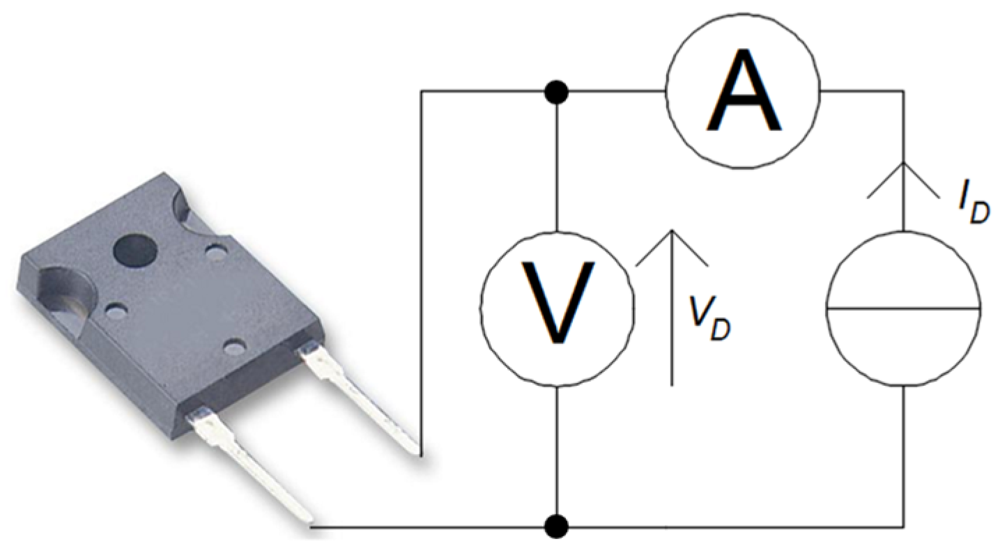
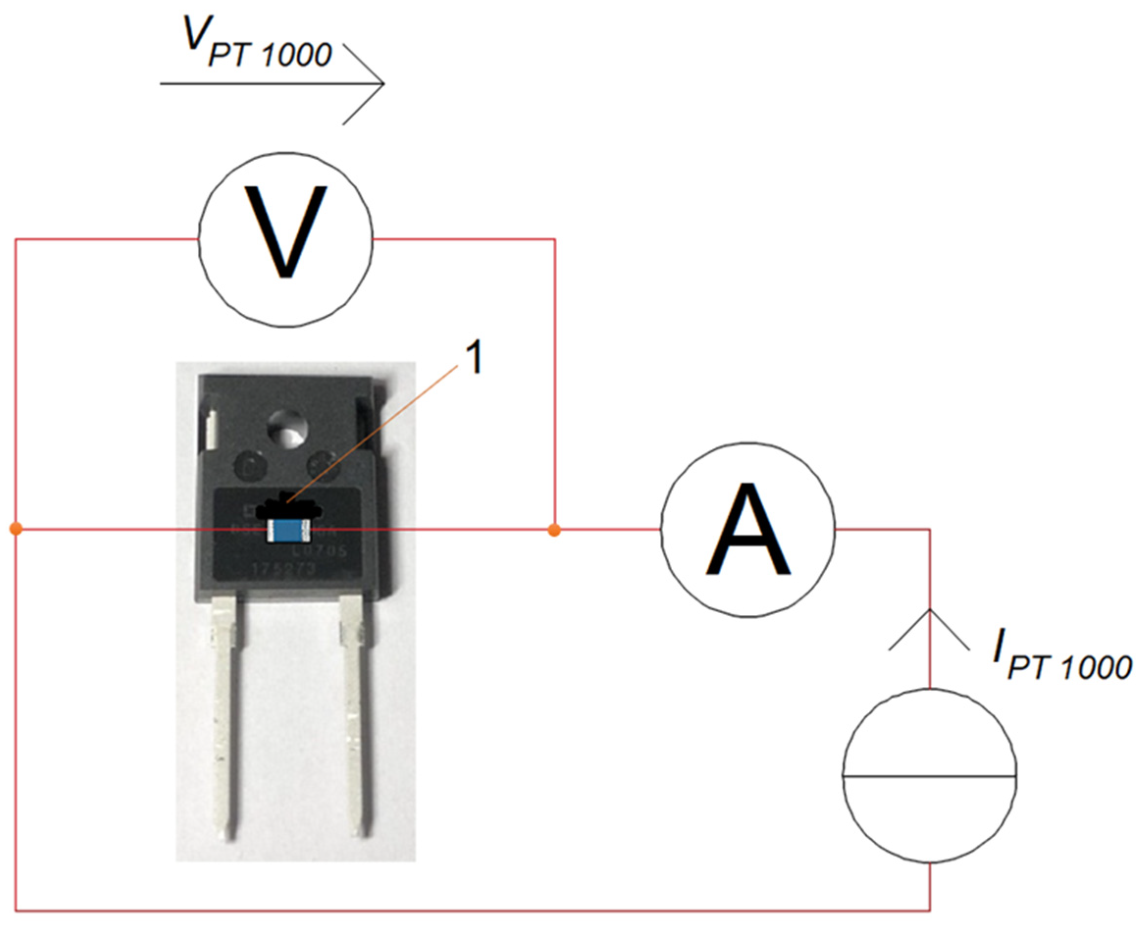
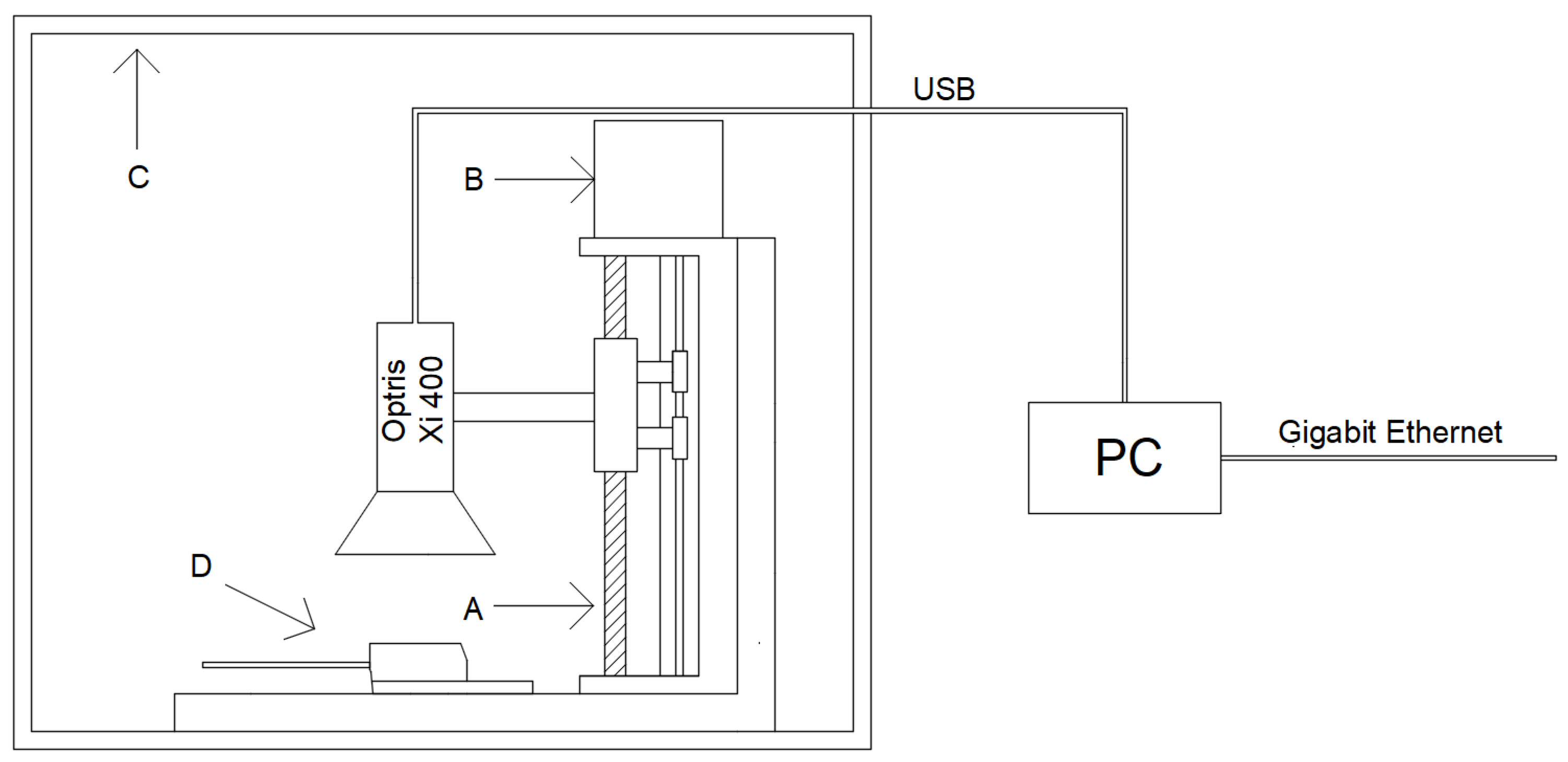
2.1. Measurement System

The temperature of the diode case Tc is dependent on the junction temperature Tj. In turn, Tj depends on the power dissipated in the junction Pj. A silicon carbide Schottky diode, FFSH10120A (Onsemi, Phoenix, AZ, USA) (IF = 10 A, VF = 1.5 V), placed in a TO-247 case was selected for this research. The view of the diode and the external dimensions of the TO-247 case are shown in Refs. [26,27].
The value of Pj was determined on the basis of the measurements performed, as the product of IF, the measured voltage drop at the diode terminals VD, and the cosine of the phase shift cosφ between ID and VD. ID and VD values were measured with a UT51 multimeter manual (UNI-T, Dongguan City, China).
The current measurement error ΔID and the voltage measurement error ΔVD were calculated according to the UT51 multimeter manual. Calculating the values of ΔID and ΔVD made it possible to determine the error value of the junction power measurement ΔPj in accordance with Equation (1) [28]:
Δ P j = Δ I D · V D + Δ V D · I D
The measuring system that was used to measure the Pj value is shown in Figure 1.
The case of the FFSH10120A diode that operates in the circuit shown in Figure 2 was observed with an Optris Xi 400 camera (Optris, Berlin, Germany). The Xi 400 model is equipped with a matrix with a spatial resolution of 382x288 pixels and a microscope lens (focal length F = 20 mm, minimum distance from the measured object WDmin = 0.35 m, IFOV (instantaneous field of view) = 0.9 mrad). The camera was connected to the computer via USB interface. The computer was equipped with the Windows 10 operating system, Intel Core i5-6500T processor and 16 GB RAM. The computer was connected to the Internet via gigabit ethernet. Optris PIX Connect software (Optris, Berlin, Germany) was installed on the computer to enable thermograms. The thermograms were sent via an Internet connection to computers with Optris PIX Connect software, SolidWorks 2022 (Dassault Systèmes, Vélizy-Villacoublay, France) and LabVIEW 2022 (National Instruments, Austin, TX, USA) installed.
The camera and diode were placed in a plexiglass chamber. The external dimensions of the chamber were 45 × 35 × 35 cm, while the internal dimensions of the chamber were 40 × 30 × 30 cm. The chamber restricts air exchange with the environment. The walls of the chamber do not allow visible light to pass through. The chamber walls were lined with black foam made of polyurethane. The foam used is characterized by a porous structure, and every single pore of the foam resembles the black body cavity model. The walls of the chamber walls so prepared are characterized by a high value of the emissivity factor ε = 0.95 [29] and a small value of the reflectance factor ρ. The measurement system prepared in this way is shown in Figure 2.
The measurement system prepared in this way made it possible to carry out research work, the result of which was the determination of the value of ε of the mold body [30]. For this purpose, a PT 1000 temperature sensor placed in an SMD 0603 case (Heraeus, Hanau, Germany) [31] was attached to the mold body of the FFSH10120A diode case [32]. The sensor was glued to the diode case. The WLK 5 glue (Fischer Elektronik, Lüdenscheid, Germany) with a known value of thermal conductivity k (k = 0.836 W/m·K) was used to stick the sensor to the case. The mold body was marked with a marker made of Velvet Coating 811-21 paint with a known emissivity coefficient value e ranging from 0.970 to 0.975 for temperatures within the limit of −36 °C to 82 °C. The uncertainty with which the value of the emissivity coefficient value was determined was 0.004. Figure 3 shows the placement of the PT 1000 sensor and the Velvet Coating 811-21 paint marker.
The known value of ε was entered into the thermographic camera. The temperature was then measured on the TcM marker (point 1 in Figure 4). The temperature measured on the marker was assumed to be the same as the temperature of the part of the mold body not covered with the Tc paint, which is located directly next to it. The camera lens was focused on the mold body fragment located right next to the marker. The value of ε was changed until the value of Tc was the same as the value of TcM. The value of ε for which the Tc values are equal to TcM is taken as ε of the mold body.

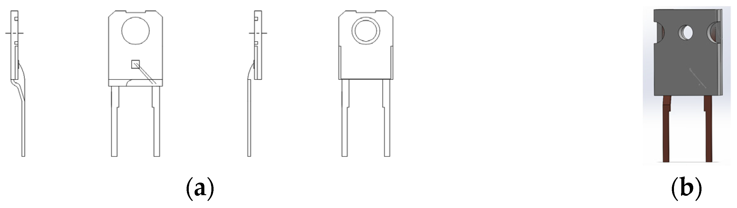
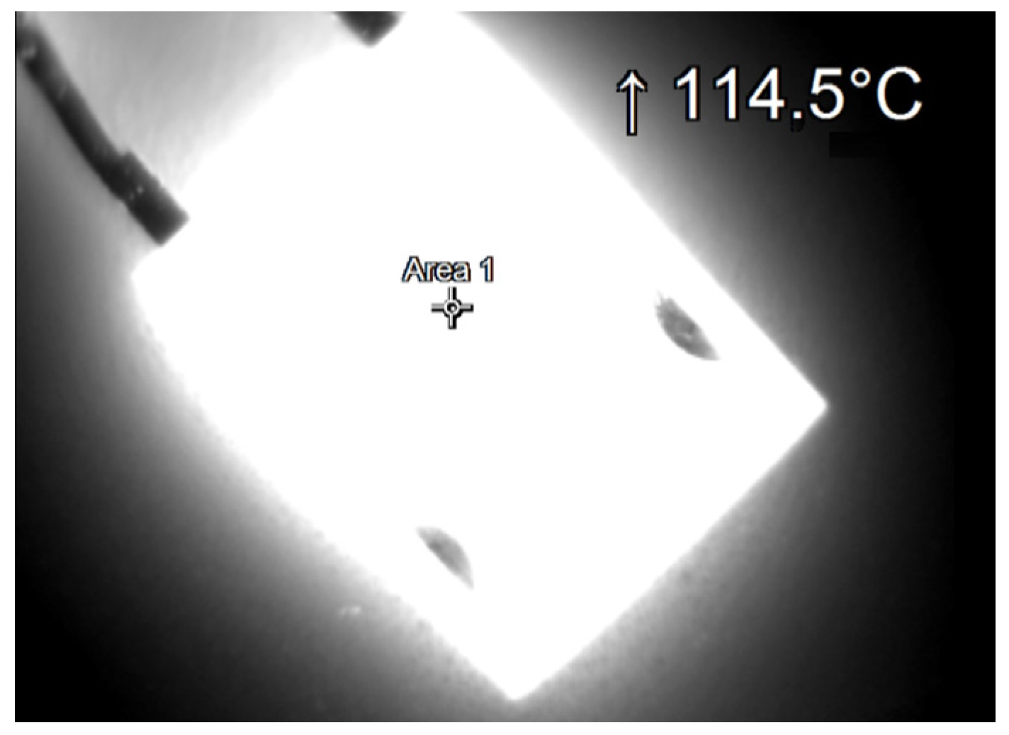
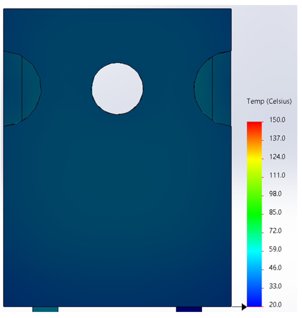
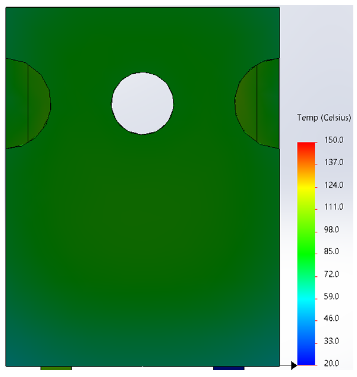
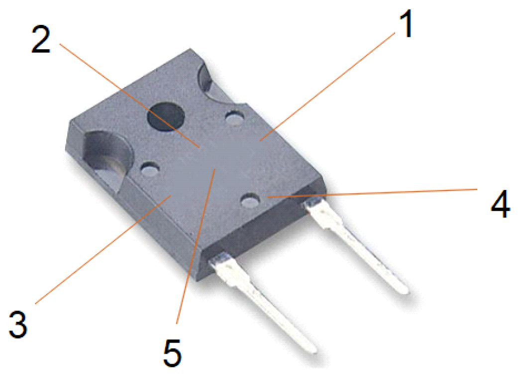
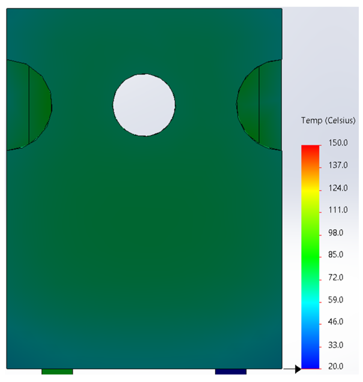
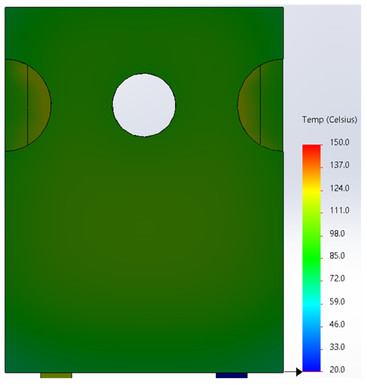
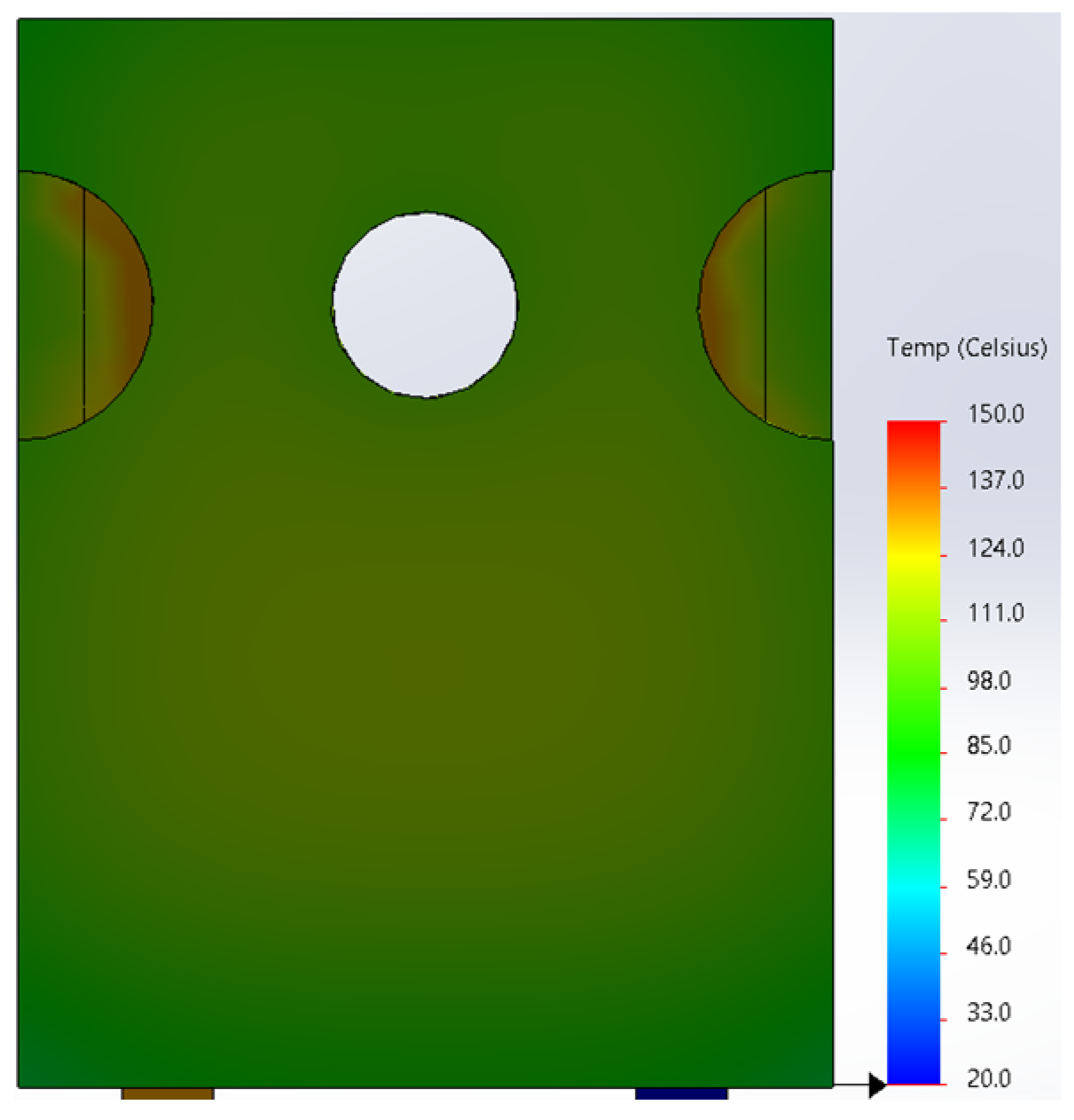
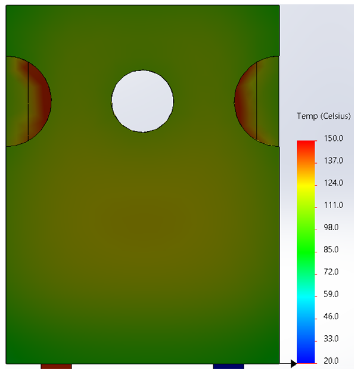
2.2. Simulations of Temperature Distribution in the TO-247 Case

In order to perform the correct simulations of the temperature distribution inside the TO-247 case, it was necessary to accurately reproduce the internal dimensions of the case. For this purpose, a mold body made of EMC (epoxy molding compound) was removed from the case. The internal dimensions were measured using a Motic Images Plus 3.0 microscope (Motic, Hong Kong, China). The internal view of the case of the FFSH10120A diode and the model made in SolidWorks are shown in Figure 4.
Heat transfer in the x direction between two points can be described by Equation (2) [33]:
q v = k · 2 T 2 x C t h · T x
where: qv is the power density dissipated in the die in W/m3, Cth is the thermal capacity, and T is the temperature.
In steady state, Equation (2) takes the form of Equation (3) [34,35].
q = k · T x
where q is the heat flux in W/m2, and k is the thermal conductivity J/Km3.
After separating the variables and integrating Equation (3) on both sides, the time constant can be obtained from the following boundary conditions (Equation (4)):
for x = 0→T = T1
for x = xkT = T2
After determining the time constant, when q penetrates the entire wall, Equation (3) takes the form of Equation (5):
T 1 T 2 = P c S · k · x
where Pc is the total power applied to the wall (W) and S (m2) is the area of the wall penetrated by J (W∙m−2).
Determining the temperature difference using Equation (5) is simple in the case of determining 1D models (the temperature difference is determined in one line). In the case of determining the temperature distribution in a solid (3D models), the number of calculations increases. The more complicated the shape of the solid, the more the number of calculations needed to determine the temperature distribution in the solid increases. In this case, numerical methods are used to determine the temperature distribution inside the solid. One of them is the finite element method (FEM). Another one of them is the FEA (finite element analysis) method. By definition, FEA is a numerical method for solving problems in engineering and mathematical physics [36].
In FEM, the area in which the temperature distribution is sought is divided into a finite number of tetrahedral elements. In each of the tetrahedral elements, the temperature field is interpolated based on the temperature in the nodes of this element and the linear shape functions are determined using Equation (6) [12]:
T x , y , z , t = i = 1 4 H i · T i t
where Ti(t) is the nodal temperature at node i, Hi is the linear shape function.
In the case of a Cartesian coordinate system, the linear temperature function (Equation (6)) for node i (in a tetrahedral element) can be expressed as Equation (7) [37]:
N i x , y , z = a i + b i · x + c i · y + d i · z
where i = 1,…,4., ai, bi, ci and di—the coefficients.
Consequently, a system of equations can be obtained for the unknown coefficients. This procedure should be repeated for all grid points. After the shape function is derived and integrated, a discrete system of equations can be obtained. When the direction of the edge of a tetrahedral element does not coincide with the direction of any axis of the coordinate system, the calculation becomes more complicated. In this case, each point, x, y and z of the original coordinate system should be changed to another point (ξ, η, ζ) in the transformed coordinate system, whose axis directions are consistent with the edge of the tetrahedral element—Equation (8) [38]:
x = x 1 + x 2 x 1 · ξ + x 3 x 1 · η + x 4 x 1 · ζ y = y 1 + y 2 y 1 · ξ + y 3 y 1 · η + y 4 y 1 · ζ z = z 1 + z 2 z 1 · ξ + z 3 z 1 · η + z 4 z 1 · ζ
The equations J of the Jacobi matrix can be described by Equation (9):
J = x 2 x 1 x 3 x 1 x 4 x 1 y 2 y 1 y 3 y 1 y 4 y 1 z 2 z 1 z 3 z 1 z 4 z 1
Shape functions for the transformed coordinate system can be written using Equation (10) [38]:
N 1 ξ ,   η ,   ζ = 1 ξ η ζ N 2 ξ ,   η ,   ζ = ξ N 3 ξ ,   η ,   ζ = η N 4 ξ ,   η ,   ζ = ζ
Performing correct simulations of the temperature distribution in the case of a semiconductor element requires determining the amount of heat emitted by radiation (through thermal radiation) and released by convection. The amount of heat given off by the radiation per unit of time per unit of area is determined by the radiation coefficient hr. The value of the radiation coefficient can be obtained using Equation (11) [39]:
h r = ε · σ c · ( T c + T a ) · ( T c 2 + T a 2 )
where σc is the Stefan–Boltzmann constant equal to 5.67 × 10⁻⁸ (W∙m−2∙K−4)), Tc is the case temperature (K) and Ta is the air temperature (K).
The value of the convection coefficient hc determines the amount of heat released by the convection per unit of time per unit of area. The hc value is difficult to determine, as it depends, among other things, on the shape, complexity and temperature of the object that gives off heat by convection. The hc coefficient was selected using the theory of similarity to physical phenomena. Relationships with physical quantities characterizing a given phenomenon were described using the criteria of Nusselt, Grashof and Prandtl. When determining the convection coefficient for a flat surface, Equation (12) [40] is used:
h c = N u · k L
where hc is the convection coefficient of flat surfaces, Nu is the Nusselt number (−) and L is the characteristic length in meters (for a vertical wall, it is its height).
The Nusselt number can be expressed using Equation (13) [41]:
N u = a · G r · P r b
where a and b are dimensionless coefficients, the values of which depend on the shape and orientation of the analyzed surface and the product Pr · Gr. Pr (−) is the Prandtl numer, Gr is the Grashof number.
The values of the coefficients a and b depend on the product of the numbers Gr and Pr of the orientation of the surface for which the hc value is calculated and the way the air flows around the surface (laminar flow, turbulent flow). The values of the coefficients a and b can be read in Table 1.
The Prandtl number can be obtained using Equation (14) [18]:
P r = c · η k
where c is the specific air heat equal to 1005 (J∙kg−1∙K−1) in 293.15 (K), η is the dynamic air viscosity equal to 1.75 × 10⁻⁵ (kg∙m−1∙s−1) in 273.15 (K).
Grashof’s number is obtained from Equation (15) [42]:
G r = α · g · T S T a · ρ 2 · L 3 η 2
where α is a coefficient of expansion equal to 0.0034 (K−1), g is the gravitational acceleration of 9.8 (m∙s−2), ρ is air density equal to 1.21 (kg∙m−3) in 273.15 (K).
In the event that the velocity of the air around a semiconductor case is faster than 0.5 m/s (e.g., due to the use of a fan), it is necessary to calculate the Nusselt number with another criteria number, and that is the Reynolds number. In this research, only natural convection was considered. For this reason, the authors refrained from describing the calculation of the Reynolds and Nusselt numbers for forced convection. The presented methods for obtaining the convection coefficient are approximate methods. In order to obtain a better factor, it is necessary to carry out further research.

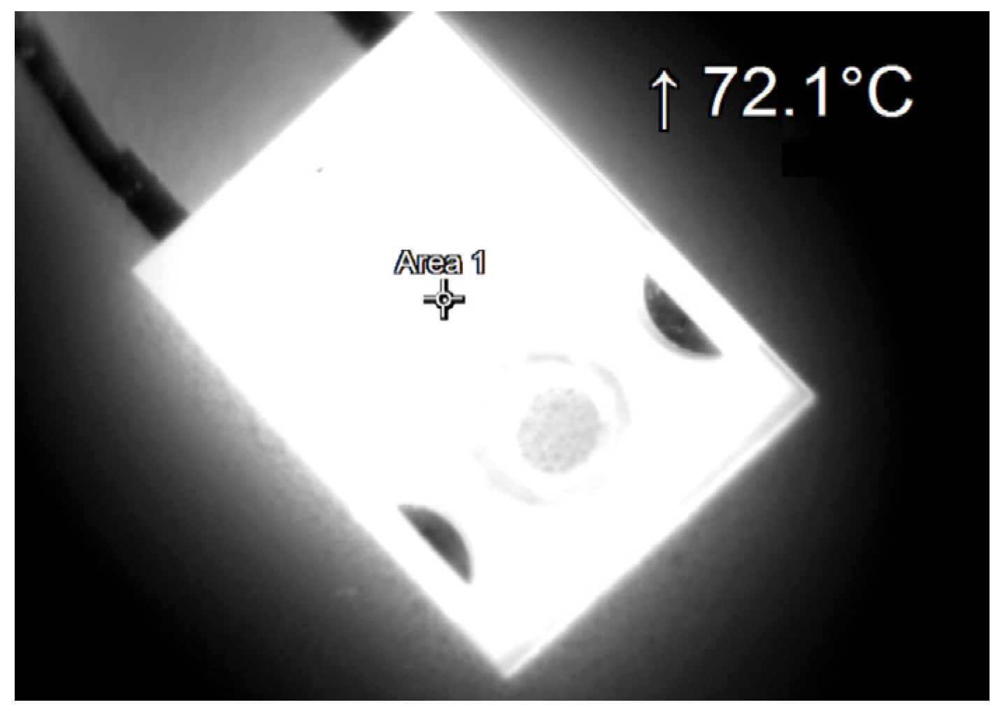
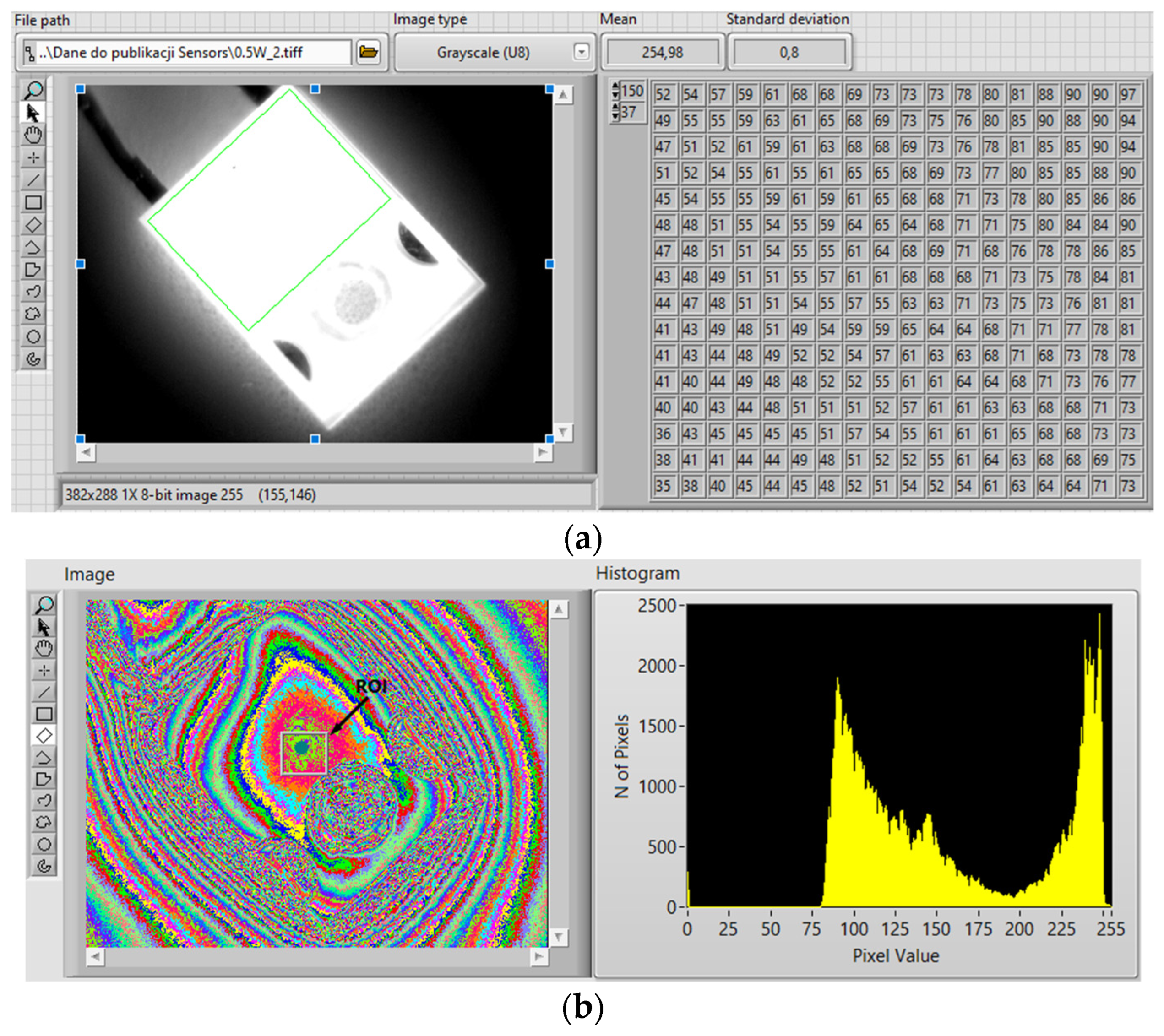
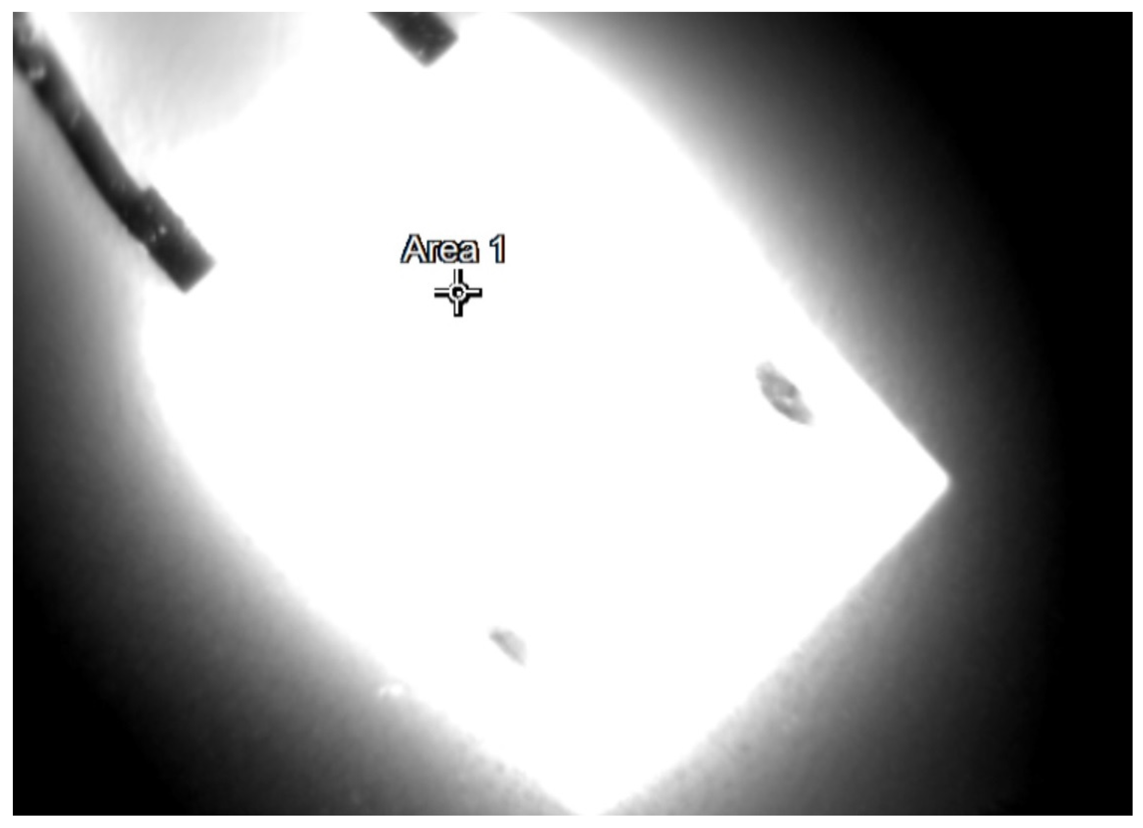
2.3. Image Processing in LabVIEW
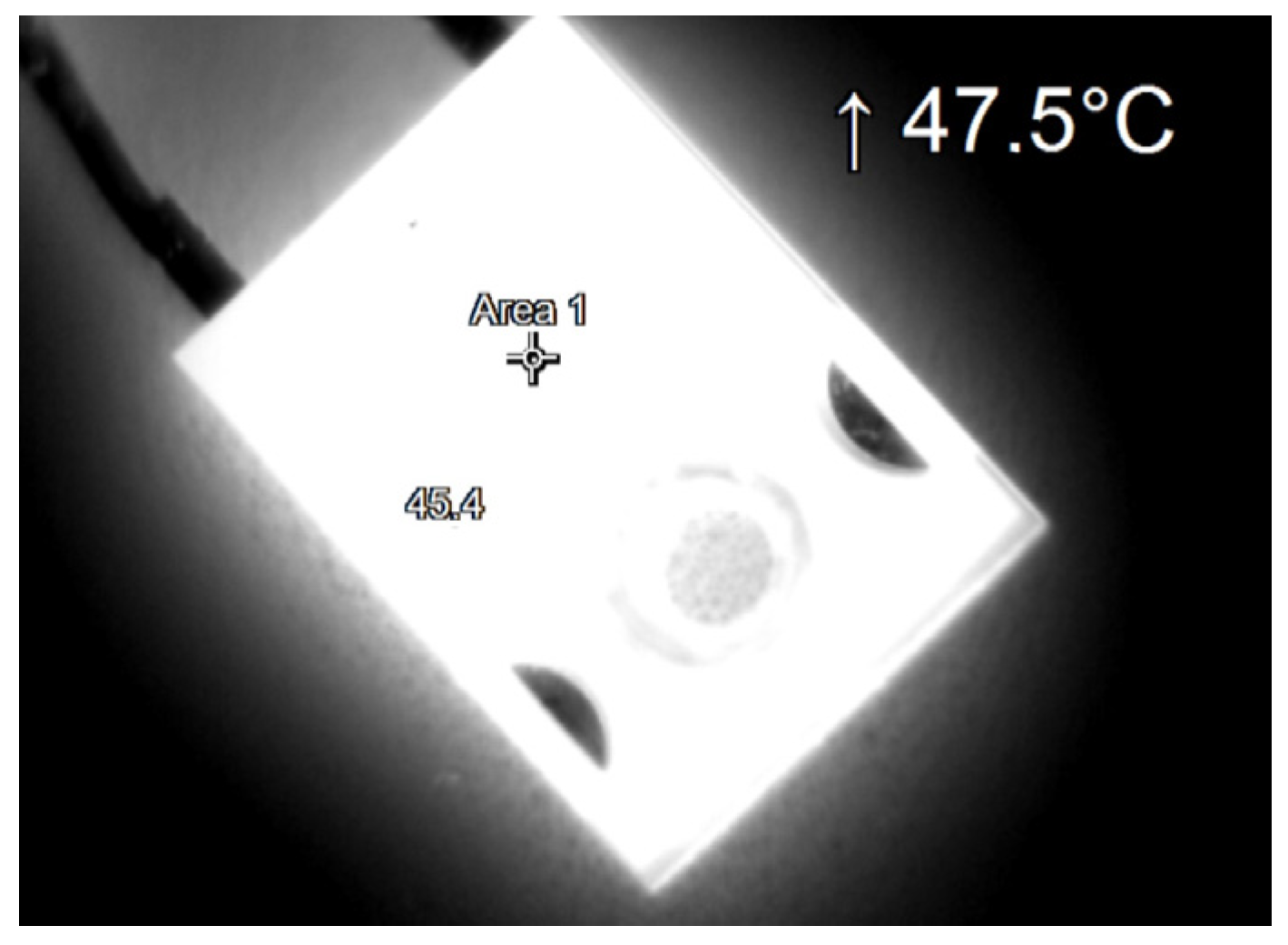
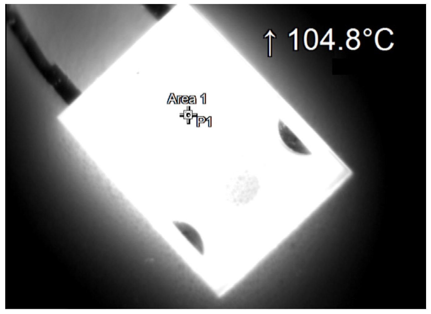
Thermographs obtained with the Optris Xi400 thermographic camera (Optris, Berlin, Germany) were analyzed. First, they were digitally processed. This made it possible to sharpen the edges of the observed semiconductor element. It was also possible to indicate a point on the mold body (the black part of the case) where the highest temperature was recorded. According to the assumptions, the temperature value in this place should be as close to the die temperature as possible. For this purpose, an image with a resolution of 382 × 288 pixels and color depth of 24 bits was obtained from a thermographic camera. To process such an image, a program was developed in the graphic programming environment LabVIEW by using National Instruments with the IMAQ package [43,44].
The created program is adapted to process files of typical formats such as BMP, TIFF, JPEG, PNG, etc. LabVIEW, using the IMAQ Create library, creates a temporary location in the computer’s memory for image processing. After the image is loaded, the pixels are automatically converted to the format set by the user. The paper presents the results after the conversion to a monochrome unsigned 8-bit format. The pixel color obtained in this way ranges from 0 to 255, with 0 being black and 255 being white. The image created as a result of the conversion is the so-called reference image [45,46].
The reference image is provided to subsequent subprograms (subVIs) that are in the code of the main program to process the information stored in it. The reference image then is visualized. In addition, it is also converted to a matrix in which pixel color values are entered. The data contained in the pixel matrix is used to create a histogram. The histogram shows the number of pixels in a given grayscale color. The program uses the function of extracting a fragment from an image selected by the user. This can be achieved by using the mouse cursor or by defining an array of four coordinates of the cut area. This functionality was introduced to avoid misinterpretation of the temperature of neighboring areas. In the observation field of the camera, there are materials with different emissivity coefficients. The emissivity coefficient set in the camera menu corresponds to the surface of the diode case. The temperature read for neighboring materials may not be correct. The result may be underestimated or overestimated. The area extracted from the entire image is then trimmed to narrow the set of hot pixels.
Using thresholding, the region of interest (ROI) with the highest temperature is designated. The color values of this area are presented in the next histogram. In addition, the average color value, the standard deviation, the minimum and maximum values for this area are calculated and displayed. The given values indirectly determine the temperature distribution around the mean value; the larger the standard deviation, the more dispersed the data is, and the more diverse the area is too. Figure 5a shows the panel of the executed program with the results of processing an example image from a thermographic camera. Figure 5b shows the converted image with real grayscale and its histogram (the gray rectangle is the ROI with the highest temperature, and the green point is the spot with the maximum temperature of the object).

3. Results

Case thermograms used in the research were made in the measuring system shown in Figure 3. In such a system, the camera was placed at a distance of 300 mm from the tested object. The thermographs were acquired remotely using Optris PIX Connect software. The obtained thermograms were subjected to further mathematical analysis. SolidWorks and LabVIEW software were used for this purpose. In addition to precise dimensioning of the tested object, thermal simulations in SolidWorks software required knowledge of the hc, ε coefficients and the power dissipated in the die. The hc coefficients were determined on the basis of Equations (12)–(15). The value of ε was determined experimentally, and the values of Pj were determined on the basis of the product of the measured IF and the voltage drop across the terminals of the diode VD. The values of ΔPj were determined on the basis of the Equation 1 and the values of ΔID and ΔUD were determined based on the instruction UT51 [47]. The results obtained are presented in Table 2.
The values of the other coefficients related to the materials used for the construction of the diode are presented in Table 3. The parameters of these coefficients are necessary for performing thermal simulations.
During the tests, thermographic measurements of the diode case were made for the several selected values of the power Pj dissipated in the die. The thermograms recorded during the measurements are shown in Figure 6, Figure 7, Figure 8, Figure 9, Figure 10 and Figure 11.
Based on the knowledge of the parameters related to the construction of the tested diode, its model was developed in SolidWorks. On this basis, the thermal simulations were performed for all values of the power dissipated in the die Pj, for which the thermographic measurements were taken earlier. The temperature distributions obtained as a result of the simulations are shown in Figure 12, Figure 13, Figure 14, Figure 15, Figure 16 and Figure 17.
Using LabVIEW 2022 software, the hottest point on the mold body was numerically determined for each Pj value. In addition, four points were selected for the mold body, located at the edges. The location of the selected points and the numerically determined hottest point on the mold body are shown in Figure 18.
The temperature values obtained on the basis of thermographic TcT measurements in the selected places and in the numerically designated warmest place were compared with the temperature values obtained at the same points of the mold body based on simulations in SolidWorks TcS. The values obtained are presented in Table 4.
For each of the selected points, the die TjS temperature and the temperature differences between the TcS case temperature, determined by the simulation, and the TjS die temperature values determined on the basis of these simulations, were determined on the basis of the simulations. The results obtained are presented in Table 5.

4. Discussion

The size of the case, the mold body and the internal dimensions of semiconductor elements depend on the type of the case. The ratio of the size of the case to the size of the mold body differs too. However, the external dimensions of the case are standardized. Therefore, the temperature gradient between two points of a semiconductor element (located vertically or horizontally, relative to each other) depends on the location of these points and the distance between them. For different types of cases, the temperature differences between the case and the surface of the mold body on which the die is placed, determined in different places in this case, are different from each other. A smaller value of this difference allows for the estimation of the die temperature value with greater accuracy. Therefore, it was necessary to find an area on the surface of the mold body where the recorded temperature would have the highest values.
In the work carried out, the Optris Xi400 thermographic camera was used. For this model, it is possible to record thermograms with a maximum frequency of f = 80 Hz. When the temperature distribution of the recorded thermograms is analyzed using LabVIEW 2022 software, it is possible to automatically find the warmest area of the mold body of the diode, in which the temperature is closest to the temperature of the die. The results of this work were confirmed by the simulation works carried out using SolidWorks software. Both the simulation work and the algorithm developed in LabVIEW determined the same area for the mold body of the diode.

5. Conclusions

During thermographic measurements of semiconductor elements, the size of the element is a significant obstacle. The mold bodies commonly used today are small in size, making thermographic measurement of the temperature of such a surface problematic. The greater the distance between the mold body and the lens of the thermographic camera, the more difficult it is to perform such a measurement.
In practice, the place on the diode mold body is more important. The temperature of a place, which is above the die, may vary more than the temperature of another place on the diode mold body, and the variation may be greater than 20 °C. The differences increase when power dissipation in the die increases (Table 5). The die temperature estimated on the basis of such a thermographic measurement (in a place on the diode mold body, which is not above the die) is burdened by a significant error.
When the tests were conducted, it was also noticed that the temperature distribution on the surface of the mold body of the semiconductor element was heterogeneous. Therefore, it can be assumed that the temperature distribution on the surface of the die is also heterogeneous. This is related, among others, to the heterogeneity of heat propagation and the irregularity of the ε value. The die is not located under the entire surface of the mold body, as a result of which different points on the case of the semiconductor device may have different temperatures. To minimize the error of die temperature estimation based on the temperature distribution of the mold body recorded using a thermographic camera, the area with the highest temperature should be found in the thermogram.
Manual determination of such an area can result in an incorrect assessment of the warmest area, especially when it is small in size. For this reason, a method has been proposed to automate this activity. The use of LabVIEW software enables the precise and automatic determination of the case area with the highest temperature shown on the recorded thermogram. As a result, the difference between the mold body temperature and the die temperature is the smallest (see Table 4 and Table 5). Therefore, the error in estimating the die temperature on the basis of an indirect thermographic measurement is thus minimized. The proposed method allows us to obtain repeatable results. The results of the work carried out confirmed the simulation work carried out on the model of the tested element, for the same values of power Pj dissipated on the die as in the thermographic measurements. The results obtained might be used in the uncertainty budget of the indirect thermographic temperature measurement of the semiconductor die.
On the basis of the conducted works, it was found that the smallest differences between the die temperature and the case temperature occur at point 5 for the model shown in Figure 18, and this is a spot on the mold body surface above the die. In the remaining points, the differences are greater, with the largest ones in point 4 of this model. The proposed method makes it possible to automate the determination of the area on the case surface of a semiconductor element where the temperature recorded by thermography is the highest. This method can be particularly useful when assessing the temperature of semiconductors based on thermographic measurements of moving elements. In this case, the time to determine the area with the highest temperature is the shortest, and the precision of this determination the highest.
The presented results are the outcome of research on temperature differences between the part of the diode mold body above the die and the diode mold body above the base plate. This information was difficult to find for FFSH 10120A. The result was obtained for one diode case and was confirmed for three other cases. The consequence was a necessity to find a method that allowed us to obtain this information.
This method can be used with other cases of the TO case family. The works carried out are an introduction to further work, as a result of which, a methodology for the remote, indirect thermographic measurement of the die temperature of a semiconductor element will be developed too. The developed method will speed up the diagnostic process and help verify the selection of the cooling system. The result of further work will also be a miniaturized measurement system for real-time integration. A diode in a TO-220-2 case was used in the work carried out. It is one of many commonly used cases. For this reason, it is necessary to conduct further research, which will allow the relationship between the temperature of the mold body and the die temperature of those cases to be determined, as presented in this article. These works will expand the area of application of the proposed method.
In this research, a cooling system was used based on natural conditions. This type of cooling system may not be sufficient in all cases (e.g., for high-power electronics). Forced convection cooling systems are more efficient. These systems require electricity to operate. In the future, there may possibly be a problem with the delivery of cheap electrical energy from ecological sources. It is necessary to reduce electricity consumption. For this reason, it is interesting to investigate the relationship between the consumption of electrical energy and the efficiency of cooling systems.

Author Contributions

K.D., A.H. and Z.K.; literature review, K.D. and A.H.; literature analysis, K.D. and A.H.; investigation, K.D., A.H. and Z.K.; resources, K.D.; writing—original draft preparation, K.D., A.H and Z.K.; writing—review and editing, K.D., A.H. and Z.K.; visualization, K.D.; supervision, K.D. and A.H. All authors have read and agreed to the published version of the manuscript.

Funding

This research was funded by the Ministry of Education and Science of Poland, grant numbers 0212/SBAD/0593 and grant numbers 0212/SBAD/0595.

Institutional Review Board Statement

Not applicable.

Informed Consent Statement

Not applicable.

Data Availability Statement

Not applicable.

Acknowledgments

Not applicable.

Conflicts of Interest

The authors declare no conflict of interest.

References

  1. Abueed, M.; Athamenh, R.; Hamasha, S.; Suhling, J.; Lall, P. Effect of Fatigue on Individual SAC305 Solder Joints Reliability at Elevated Temperature. In Proceedings of the 19th IEEE Intersociety Conference on Thermal and Thermomechanical Phenomena in Electronic Systems (ITherm), Orlando, FL, USA, 21–23 July 2020; pp. 1043–1050. [Google Scholar] [CrossRef]
  2. Lu, W.-C.; Wu, C.-H.; Yeh, C.-Y.; Wu, C.-H.; Wang, C.-L.; Wang, L.A. D-Shaped Silicon-Cored Fibers as Platform to Build In-Line Schottky Photodetectors. IEEE Photonics Technol. Lett. 2021, 33, 317–320. [Google Scholar] [CrossRef]
  3. Otto, A.; Rzepka, S. Lifetime modelling of discrete power electronic devices for automotive applications. In Proceedings of the AmE 2019—Automotive Meets Electronics, 10th GMM-Symposium, Dortmund, Germany, 12–13 March 2019; pp. 1–6, ISBN 978-3-8007-4877-8. [Google Scholar]
  4. Steiner, A. 600 V CoolMOS™ P7. Infineon Technology AG, Munich, Germany, Infineon Appl. Note AN_201703_PL52_015. Available online: https://www.infineon.com/600v-p7 (accessed on 16 November 2022).
  5. Blackburn, D.L. Temperature measurements of semiconductor devices—A review. In Proceedings of the Twentieth Annual IEEE Semiconductor Thermal Measurement and Management Symposium (IEEE Cat. No.04CH37545), San Jose, CA, USA, 11–13 March 2004; pp. 70–80. [Google Scholar] [CrossRef]
  6. Plesca, A. Thermal Analysis of Power Semiconductor Device in Steady-State Conditions. Energies 2020, 13, 103. [Google Scholar] [CrossRef]
  7. Górecki, K.; Posobkiewicz, K. Cooling Systems of Power Semiconductor Devices—A Review. Energies 2022, 15, 4566. [Google Scholar] [CrossRef]
  8. Vellvehi, M.; Perpiñà, X.; Aviñó, O.; Ferrer, C.; Fusté, N.; Sánchez, D.; Jordà, X.; Godignon, P.; Massetti, S. Analysis of SiC Schottky diodes after thermal vacuum test by means of lock-in infrared thermography. In Proceedings of the 2020 21st International Conference on Thermal, Mechanical and Multi-Physics Simulation and Experiments in Microelectronics and Microsystems (EuroSimE), Cracow, Poland, 5–8 July 2020; pp. 1–6. [Google Scholar] [CrossRef]
  9. Kendig, D.; Tay, A.; Shakouri, A. Thermal analysis of advanced microelectronic devices using thermoreflectance thermography. In Proceedings of the 2016 22nd International Workshop on Thermal Investigations of ICs and Systems (THERMINIC), Budapest, Hungary, 21–23 September 2016; pp. 115–120. [Google Scholar] [CrossRef]
  10. Strąkowska, M.; De Mey, G.; Więcek, B. Comparison of the Fourier-Kirchhoff, Pennes and DPL thermal models of a single layer tissue. In Proceedings of the 15th Quantitative InfraRed Thermography Conference, Porto, Portugal, 20–23 September 2020; Available online: http://qirt.gel.ulaval.ca/archives/qirt2020/papers/127.pdf (accessed on 16 November 2022).
  11. Tzou, D.Y. Macro-to Microscale Heat Transfer: The Lagging Behavior, 2nd ed.; Wiley: Hoboken, NJ, USA, 2014; ISBN 978-1-118-81822-0. [Google Scholar]
  12. Feng, S.Z.; Cui, X.Y.; Li, G.Y. Transient thermal mechanical analyses using a face-based smoothed finite element method (FS-FEM). Int. J. Therm. Sci. 2013, 74, 95–103. [Google Scholar] [CrossRef]
  13. JESD 51-53. Available online: https://www.jedec.org/document_search?search_api_views_fulltext=13.%09JESD%2051-53 (accessed on 16 November 2022).
  14. JESD 51-14. Available online: https://www.jedec.org/document_search?search_api_views_fulltext=JESD%2051-14 (accessed on 16 November 2022).
  15. Hulewicz, A.; Dziarski, K.; Dombek, G. The Solution for the Thermographic Measurement of the Temperature of a Small Object. Sensors 2021, 21, 5000. [Google Scholar] [CrossRef] [PubMed]
  16. Zaccara, M.; Edelman, J.B.; Cardone, G. A general procedure for infrared thermography heat transfer measurements in hypersonic wind tunnels. Int. J. Heat Mass Transf. 2020, 163, 120419–120435. [Google Scholar] [CrossRef]
  17. Altenburg, S.J.; Straße, A.; Gumenyuk, A.; Maierhofer, C. In-situ monitoring of a laser metal deposition (LMD) process: Comparison of MWIR, SWIR and high-speed NIR thermography. Quant. InfraRed Thermogr. J. 2022, 19, 97–114. [Google Scholar] [CrossRef]
  18. Yoon, S.T.; Park, J.C. An experimental study on the evaluation of temperature uniformity on the surface of a blackbody using infrared cameras. Quant. InfraRed Thermogr. J. 2021, 19, 172–186. [Google Scholar] [CrossRef]
  19. Schuss, C.; Remes, K.; Leppänen, K.; Saarela, J.; Fabritius, T.; Eichberger, B.; Rahkonen, T. Detecting Defects in Photovoltaic Cells and Panels with the Help of Time-Resolved Thermography under Outdoor Environmental Conditions. In Proceedings of the 2020 IEEE International Instrumentation and Measurement Technology Conference (I2MTC), Dubrovnik, Croatia, 25–28 May 2020; pp. 1–6. [Google Scholar] [CrossRef]
  20. Chakraborty, B.; Sinha, B.K. Process-integrated steel ladle monitoring, based on infrared imagin—A robust approach to avoid ladle breakout. Quant. InfraRed Thermogr. J. 2020, 17, 169–191. [Google Scholar] [CrossRef]
  21. Tomoyuki, T. Coaxiality Evaluation of Coaxial Imaging System with Concentric Silicon–Glass Hybrid Lens for Thermal and Color Imaging. Sensors 2020, 20, 5753. [Google Scholar] [CrossRef]
  22. Wollack, J.E.; Cataldo, G.; Miller, K.H.; Quijada, A.M. Infrared properties of high-purity silicon. Opt. Lett. 2020, 45, 4935–4938. [Google Scholar] [CrossRef]
  23. Singh, J.; Arora, A.S. Effectiveness of active dynamic and passive thermography in the detection of maxillary sinusitis. Quant. InfraRed Thermogr. J. 2020, 18, 213–225. [Google Scholar] [CrossRef]
  24. Litwa, M. Influence of Angle of View on Temperature Measurements Using Thermovision Camera. IEEE Sens. J. 2010, 10, 1552–1554. [Google Scholar] [CrossRef]
  25. Dziarski, K.; Hulewicz, A.; Dombek, G. Lack of Thermogram Sharpness as Component of Thermographic Temperature Measurement Uncertainty Budget. Sensors 2021, 21, 4013. [Google Scholar] [CrossRef] [PubMed]
  26. View of TO 220 Case and TO 220 Case Dimension. Available online: https://www.onsemi.com/download/data-sheet/pdf/ffsh10120a-d.pdf (accessed on 16 November 2022).
  27. Toshiba. TO-247. Available online: https://toshiba.semicon-storage.com/ap-en/semiconductor/design-development/package/detail.TO-247.html (accessed on 16 November 2022).
  28. Cysewska-Sobusiak, A. Podstawy Metrologii i Inżynierii Pomiarowej; Wydawnictwo Politechniki Poznańskiej: Poznań, Poland, 2010. (In Polish) [Google Scholar]
  29. Krawiec, P.; Rózański, L.; Czarnecka-Komorowska, D.; Warguła, Ł. Evaluation of the Thermal Stability and Surface Characteristics of Thermoplastic Polyurethane V-Belt. Materials 2020, 7, 1502. [Google Scholar]
  30. Kawor, E.T.; Mattei, S. Emissivity measurements for nexel velvet coating 811-21 between 36 °C and 82 °C, 15 ECTP Proceedings. High Temp. High Press 1999, 31, 551–556. [Google Scholar] [CrossRef]
  31. Diselectric. Available online: https://www.distrelec.de/en/platinum-smd-temperature-sensor-pt1000-50-150-2mm-jumo-906125-pcs-1302-10-00/p/17668873 (accessed on 16 November 2022).
  32. Softronic. Available online: https://sofitronic.de/products_new2.asp?groups=Diode-TO247&gname=Diode-TO247&mname1=Diodes-Rectifier (accessed on 16 November 2022).
  33. Strąkowska, M.; Więcek, B.; De Mey, G. Identification of the Thermal Constants of the DPL Heat Transfer Model of a Single Layer Porous Material. Pomiary Autom. Robot. 2021, 25, 41–46. [Google Scholar] [CrossRef]
  34. Kopeć, M.; Więcek, B. AC temperature estimation of power electronic devices using 1D thermal modeling and IR thermography measurements. In Proceedings of the 15th Quantitative InfraRed Thermography Conference, Porto, Portugal, 20–23 September 2020; pp. 1–7. Available online: http://qirt.gel.ulaval.ca/archives/qirt2020/papers/161.pdf (accessed on 16 November 2022).
  35. Bejan, A. Heat Transfer; Wiley: New York, NY, USA, 1993. [Google Scholar]
  36. Alisibramulisi, A. Finite Element Analysis (FEA) Project in Structural Engineering Subject. In Proceedings of the 2019 IEEE 11th International Conference on Engineering Education (ICEED), Kanazawa, Japan, 6–7 November 2019. [Google Scholar]
  37. Devloo, P.R.B.; Bravo, C.M.A.A.; Rylo, E.C. Systematic and generic construction of shape functions for p-adaptive meshes of multidimensional finite elements. Comput. Methods Appl. Mech. Eng. 2009, 198, 1716–1725. [Google Scholar] [CrossRef]
  38. Ceric, H. Numerical Techniques in Modern TCAD. reposiTUm 2005, 102. Available online: https://repositum.tuwien.at/handle/20.500.12708/20403 (accessed on 16 November 2022).
  39. Li, B. Investigation and modelling of work roll temperature in induction heating by finite element method. J. South. Afr. Inst. Min. Metall. 2018, 118, 735–743. [Google Scholar] [CrossRef]
  40. Staton, D.A.; Cavagnino, A. Convection heat transfer and flow calculations suitable for electric machines thermal models. IEEE Trans. Ind. Electron. 2008, 55, 3509–3516. [Google Scholar] [CrossRef]
  41. Ghahfarokhi, P.S. Determination of Forced Convection Coefficient over a Flat Side of Coil. In Proceedings of the 2017 IEEE 58th International Scientific Conference on Power and Electrical Engineering of Riga Technical University (RTUCON), Riga, Latvia, 12–13 October 2017. [Google Scholar] [CrossRef]
  42. Aminu, Y.; Ballikaya, S. Thermal resistance analysis of trapezoidal concentrated photovoltaic–Thermoelectric systems. Energy Convers. Manag. 2021, 250, 114908. [Google Scholar] [CrossRef]
  43. IMAQ Vision for LabVIEW User Manual; October 2000 Edition, Part Number 322917A-01; National Instruments: Austin, TX, USA, 2000.
  44. IMAQ Vision Concepts Manual; June 2003 Edition, Part Number 322916B-01; National Instruments: Austin, TX, USA, 2003.
  45. Christopher, G.R. Image Acquisition and Processing with LabVIEW, 1st ed.; CRC Press: Boca Raton, FL, USA, 2003. [Google Scholar]
  46. Klinger, T. Image Processing with LabVIEW™ and IMAQ™ Vision; CRC Press: Boca Raton, FL, USA, 2003. [Google Scholar]
  47. User Manual UT51. Available online: https://www.manua.ls/uni-t/ut51/manual (accessed on 16 November 2022).
Figure 1. Measuring system used to measure the power dissipated at the Pj junction.
Sensors 23 01944 g001
Figure 2. Measurement system with Optris Xi400 camera and FFSH10120A diode: (A) tripod; (B) stepper motor; (C) chamber made of black foam made of polyurethane; (D) the observed semiconductor element.
Sensors 23 01944 g002
Figure 3. The spot to place the PT 1000 sensor on the mold body of the FFSH10120A diode and the marker made of Velvet Coating 811-21 paint—point 1.
Sensors 23 01944 g003
Figure 4. (a) Internal view of the TO-247-2 case with the FFSH10120A diode; (b) FFSH10120A diode model made in SolidWorks.
Sensors 23 01944 g004
Figure 5. (a) A panel of the executed program with the sample results of the processing image; (b) a true grayscale image and its histogram.
Sensors 23 01944 g005
Figure 6. The case thermogram of the FFSH10120A diode. The average temperature at the cursor: 45 °C. The maximum temperature at the cursor (the area is equal to 9xIFOV (instantaneous field of view)) is 47.5 °C. The power dissipated at the junction Pj = 0.57 W.
Sensors 23 01944 g006
Figure 7. The case thermogram of the FFSH10120A diode. The average temperature at the cursor: 70.4 °C. The maximum temperature at the cursor (the area is equal to 9xIFOV (instantaneous field of view)) is 72.1 °C. The power dissipated at the junction Pj = 1.32 W.
Sensors 23 01944 g007
Figure 8. The case thermogram of the FFSH10120A diode. The average temperature at the cursor: 89.6 °C. The maximum temperature at the cursor (the area is equal to 9xIFOV (instantaneous field of view)) is 91.5 °C. The power dissipated at the junction Pj = 1.71 W.
Sensors 23 01944 g008
Figure 9. The case thermogram of the FFSH10120A diode. The average temperature at the cursor: 102.4 °C. The maximum temperature at the cursor (the area is equal to 9xIFOV (instantaneous field of view)) is 104.8 °C. The power dissipated at the junction Pj = 2.19 W.
Sensors 23 01944 g009
Figure 10. The case thermogram of the FFSH10120A diode. The average temperature at the cursor: 112.2 °C. The maximum temperature at the cursor (the area is equal to 9xIFOV (instantaneous field of view)) is 114.5 °C. The power dissipated at the junction Pj = 2.55 W.
Sensors 23 01944 g010
Figure 11. The case thermogram of the FFSH10120A diode. The average temperature at the cursor: 123.8 °C. The maximum temperature at the cursor (the area is equal to 9xIFOV (instantaneous field of view)) 125.4 °C. The power dissipated at the junction Pj = 3.01 W.
Sensors 23 01944 g011
Figure 12. The simulation result for the case of the FFSH10120A diode. The maximum recorded temperature: 47.2 °C. The power dissipated at the junction Pj = 0.57 W. The temperature ranges from 20 °C to 150 °C.
Sensors 23 01944 g012
Figure 13. The simulation result for the case of the FFSH10120A diode. The maximum recorded temperature: 72.5 °C. The power dissipated at the junction Pj = 1.32 W. The temperature ranges from 20 °C to 150 °C.
Sensors 23 01944 g013
Figure 14. The simulation result for the case of the FFSH10120A diode. The maximum recorded temperature: 90.6 °C. The power dissipated at the junction Pj = 1.71 W. The temperature ranges from 20 °C to 150 °C.
Sensors 23 01944 g014
Figure 15. The simulation result for the case of the FFSH10120A diode. The maximum recorded temperature: 103.6 °C. The power dissipated at the junction Pj = 2.19 W. The temperature ranges from 20 °C to 150 °C.
Sensors 23 01944 g015
Figure 16. The simulation result for the case of the FFSH10120A diode. The maximum recorded temperature: 115.0 °C. The power dissipated at the junction Pj = 2.55 W. The temperature ranges from 20 °C to 150 °C.
Sensors 23 01944 g016
Figure 17. The simulation result for the case of the FFSH10120A diode. The maximum recorded temperature: 125.0 °C. The power dissipated at the junction Pj = 3.01 W. The temperature ranges from 20 °C to 150 °C.
Sensors 23 01944 g017
Figure 18. The location of the selected points on the mold body, the black part of the diode case made of epoxy resin (1–4) and the numerically designated place of the hottest spot on mold body 5. Point 5 was placed in the center of the lower part of the mold body (area below the circular holes).
Sensors 23 01944 g018
Table 1. Natural convection correlation coefficients [41]; alam is the value of coefficient a for laminar flow, blam is the value of coefficient b for laminar flow, aturb is the value of coefficient a for turbulent flow, and bturb is the value of coefficient b for turbulent flow.
ShapeGr∙Pralamblamaturbbturb
Vertical flat wall1090.590.250.1290.33
Upper flat wall1080.540.250.140.33
Lower flat wall1050.250.25NANA
Table 2. The power Pj values dissipated in the die, the current flowing through the ID junction, the measurement error of the current flowing through the ΔID junction, the voltage at the diode terminals VD, the voltage measurement error at the diode terminals ΔVD, the value of ε mold body and the value of the convection coefficient hc.
Pj
(W)
ID
(A)
ΔID
(A)
VD
(V)
ΔVD
(V)
ΔP
(W)
ε
(−)
hc
(−)
0.570.530.021.070.020.030.977,51
1.321.080.031.220.020.050.978.53
1.711.470.031.160.020.060.969.03
2.191.780.041.230.020.070.969.34
2.551.990.041.280.020.080.959.62
3.012.260.041.330.020.100.919.91
Table 3. The parameters related to the materials used to build the tested diode.
Fragment of the Casek
(W/m·K)
The Material
(−)
Mold body0.25The EMC material
The back of the case400.00Copper
The die150.00Silicon carbide
Leads400.00Copper
The material under the die400.00Copper
Table 4. The thermography-measured case temperature values TcT and the simulation results obtained in SolidWorks TcS for each of the points are shown in Figure 18.
Point12345
Pj
(W)
TcT
(°C)
TcS
(°C)
TcT
(°C)
TcS
(°C)
TcT
(°C)
TcS
(°C)
TcT
(°C)
TcS
(°C)
TcT
(°C)
TcS
(°C)
0.5743.5 44.144.8 46.043.7 44.341.2 41.345.7 47.2
1.3266.4 67.169.2 69.567.1 67.360.0 60.672.1 72.5
1.7181.3 80.685.4 86.680.8 81.971.5 71.291.5 90.6
2.1995.0 94.596.6 97.392.9 94.682.1 81.9104.8 103.6
2.55102.8 103.3109.8 109.1103.7 104.791.6 91.8114.5 115.0
3.01113.6 114.2117.2 118.1115.3 116.797.7 97.2125.4 125.0
Table 5. Die temperature TjS and the differences between TcS temperature and die TjS temperature determined on the basis of the simulation.
Point12345
Pj
(W)
TjS
(°C)
TjS–TcS
(°C)
TjS–TcS
(°C)
TjS–TcS
(°C)
TjS–TcS
(°C)
TjS–TcS
(°C)
0.5751.77.65.77.410.44.5
1.3282.415.312.915.121.89.9
1.71104.523.917.922.633.313.9
2.19120.525.023.225.938.616.9
2.55134.931.625.830.243.119.9
3.01148.734.530.632.051.523.7
Disclaimer/Publisher’s Note: The statements, opinions and data contained in all publications are solely those of the individual author(s) and contributor(s) and not of MDPI and/or the editor(s). MDPI and/or the editor(s) disclaim responsibility for any injury to people or property resulting from any ideas, methods, instructions or products referred to in the content.

