Abstract
The design of a photonic system for the trapping and waveguiding of ultracold atoms far above a dielectric surface is proposed and analyzed. The system consists of an optical rib waveguide deposited on a planar one-dimensional photonic crystal, which sustains two wavelengths of photonic crystal surface modes tuned in the red and blue sides relative to the atomic transition of the neutral atom. The addition of a third blue-tuned wavelength to the system allows the neutral atoms to be stabilized in the lateral dimension above the rib waveguide. Trapping atoms at relatively large distances, more than 600 nm above the dielectric surface, allows to reduce the influence of Casimir–Polder forces in this system. The detailed design methodology and specifications of the photonic system are provided. The presented design can be employed in atomic chips and quantum sensors.
1. Introduction
The development of quantum sensors [1] based on coherent atomic circuits is important for the realization of many potential technological applications [2], such as gravimeters [3,4,5,6,7], gradiometers [8] and gyroscopes [9,10]. Atom chips [11,12,13] provide a versatile technique for the generation and coherent manipulation of ultracold atoms for such sensors on the micrometer scale.
For the successful development of compact and robust atom chips integrated with guided atomic interferometers, the optimal choice of the appropriate interface for the light–atom interaction is of crucial importance. In this study, we examine the trapping and waveguiding of ultracold atoms employing two-color optical surface waves propagating along the external boundary of a rib waveguide located on top of a specially designed planar one-dimensional photonic crystal (1D PC).
The use of optical waveguides to guide atoms was proposed in 1993 by Letokhov et al. [14]. They proposed to create a potential well inside a hollow core fiber by a laser with a red-detuned light directed into the fiber. Since then, the use of optical waveguides has been identified as a key element of atomic chip interferometry, and many types of optical waveguides have been considered as candidates for the best interfaces of light–atom interactions within them. The employment of integrated optical waveguides to trap and guide ultracold atoms above planar surfaces has been analyzed in [15,16]. They exploit an earlier proposal by Ovchinnikov et al. [17] to use two colors of light, with red and blue detuning and different evanescent decay lengths, to obtain a planar (one-dimensional) trap with a potential minimum above a dielectric prism. That is, the insertion of optical waveguides into a planar surface should add lateral confinement and restrict the ensemble of cold atoms in two dimensions.
The main problem here is that the evanescent decay length into an external medium in such waveguides cannot be very large, since the effective refractive index of an optical wave in a standard waveguide cannot be smaller than the refractive index of the waveguide substrate . The penetration length of the evanescent wave intensity (i.e., ) in the external medium is
Here, is either the numerical aperture of the light beam in the prism, , or the effective refractive index of the optical mode in the corresponding planar 1D slab waveguide, . The refractive index of the external medium (i.e., a vacuum for atom optics applications) is . The value of can only be very large in the case when the difference is small.
It is shown below that this condition can be satisfied for a photonic crystal (PC) waveguide, in contrast to a standard optical waveguide. It is this unique property of PC waveguides that makes it possible to design the photonic system that sustains the ultracold atomic ensembles at relatively large distances above the dielectric surface. This is the reason why, in this communication, we propose and analyze such an innovative waveguide structure, based on planar 1D PC, for ultracold atom trapping and waveguiding.
2. Materials and Methods
2.1. Planar Photonic Crystal Waveguides and Their Differences from Standard Waveguides
The effective index of a two-dimensional optical waveguide with finite lateral width (i.e., rib or ion-implanted waveguide) is somewhat smaller than the effective index of the corresponding planar 1D slab waveguide , where the width of (i.e., extends to infinity in the lateral direction). This diminution of is due to the zigzag propagation (from left to right) of the wave in the plane of the waveguide (in the ray model approximation), resulting in a reduction in the projection of the wavevector in the z-direction. But the penetration length of the waveguide mode intensity into the external medium for a two-dimensional waveguide is still determined by the Formula (1), where the effective index of the corresponding planar 1D slab waveguide is inserted as .
According to Equation (1), only modes with can have large penetration length in the medium with . In standard waveguides, the optical field confinement in the vertical direction is the result of total internal reflection (TIR) on both sides of the waveguide layer. As a result, (i.e., ), and the maximum possible penetration length cannot be greater than . For a waveguide on a quartz substrate with and nm, this gives nm. In [15], the authors consider sodium fluoride (the lowest-index common optical mineral, ) as a possible substrate, but it yields only nm.
One possible way to mitigate this limitation is to use a freely suspended thin dielectric film [18,19] to achieve . With this approach, the following penetration length values for the intensity of evanescent waves were obtained [18]: nm and 69.75 nm for modes excited in a 300 nm thick suspended silica film with waveguide rib height nm and width m (at wavelengths nm and 720 nm, respectively).
This communication presents a different approach to overcome this limitation, in which the uniform waveguide substrate is replaced by a planar 1D photonic crystal, which is designed to create a photonic bandgap in the spectral region of interest. Thus, in this case, the optical field confinement in the vertical direction is due to reflection from the photonic bandgap on one side (bottom) and total internal reflection—as usual—on the another side (top) of the waveguide, as shown in Figure 1.
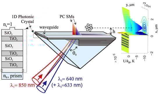
Figure 1.
Concept of the photonic system under consideration: the left inset shows the cross-section of the 1D PC structure, and the right inset shows the outline of the well trap potential for ultracold atoms.
The planar 1D PC is a simple dielectric stack. It is durable and compatible with existing technologies for producing dielectric mirrors; so, its fabrication is much easier than suspended thin dielectric films. In the vicinity of the interface between the planar 1D PC and the external medium, optical surface waves can be excited subject to an appropriate choice of the thicknesses of the double layers and the thickness of the final truncated layer [20].
These optical surface waves are excitations of photonic crystal surface modes (PC SMs), also known as ‘(asymmetric) planar Bragg waveguide modes’, ‘surface waves in periodic layered media’, ‘photonic bandgap surface modes’, ‘optical Bloch surface waves’, ‘photonic crystal surface waves’ and ‘surface waves in multilayer coatings’. They were first studied both theoretically [21,22] and experimentally [23] in the 1970s. Twenty years later, the excitation of optical surface modes in the Kretschmann-like configuration was demonstrated [24,25]. In recent years, PC SMs have found an increasing number of applications in the fields of optical sensors [26,27,28,29,30] and optical biosensors [31,32,33,34,35,36,37], as well as other fields [38,39,40,41,42,43].
The penetration length in the external medium can be very large for these modes, as their effective refractive index can be infinitesimally close to the refractive index (RI) of the external medium. This is a unique property of PC SMs that makes their excitation with quite possible. In the first optical biosensor based on these modes [31], this property was already used to distinguish between a surface adsorption and bulk RI (i.e., RI far from the surface).
2.2. Design Methodology for a 2D Waveguide Placed on a 1D PC
2.2.1. Design of a 1D PC
The design of a 1D PC, sustaining two PC SMs at wavelengths nm and nm, was performed using a free Windows program available at [44]. Results are presented in Figure 2. The wavelengths are chosen to be detuned far enough away from the , transitions of the Rb atom ( nm, nm) on the blue and the red sides. The light potential (which causes the attraction and repulsion forces) scales as , while the light scattering rate (which causes the heating rate) scales as [45], where is a detuning from the D transitions (see Equations (3) and (4) below). Therefore, to increase the trap lifetime, it is better to be away from the resonance if the intensities still allow the desired trap depth to be reached. The larger detuning in the blue side is due to the expectation that a larger value of intensity of the repulsive (blue-detuned) light beam will be needed to form a well trap potential of the desired shape.
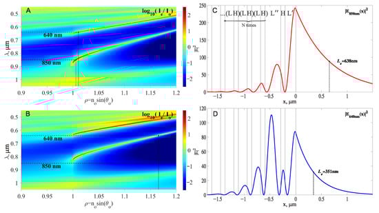
The following 1D PC structure is designed to sustain both nm and nm PC SMs:
where L is the layer (thickness nm), H is the layer (thickness nm), is the extended layer (thickness nm) and is the final layer (thickness nm). The upper part of Figure 2C shows the embedded representation of the structural Formula (2). The RIs of , layers used in the calculations are given in Table 1. The obtained parameters of PC SMs in this planar 1D PC structure are also presented in Table 1 and in Figure 2.

Table 1.
The RIs of the dielectric layers and the PC SMs parameters for the planar 1D PC.
It can be seen that this 1D PC is designed so that both modes at nm have an excitation angle very close to the TIR angle, and hence, the effective RI is close to unity (). As a consequence, the penetration lengths of their intensities into the vacuum are very long (see in Figure 2C,D and in Table 1).
2.2.2. From 1D PC Waveguide to 2D Waveguide
Note that if we reduce the thickness of the final layer by 25 nm (or more), from nm to 182 nm, then no PC SMs will be excited on such planar 1D PC near (up to for nm); see Figure 2B. Therefore, if we use the planar 1D PC with nm and a waveguide of height nm above it, the excitation of the PC SMs will take place inside the two-dimensional waveguide only, subject to its width being sufficient. Thus, if excitation is performed by beams with excitation angles close to , then only PC SMs with will be excited, i.e., only modes in two-dimensional waveguides of width but not modes in the surrounding planar slab waveguide. Moreover, the penetration of such a waveguide wave into the external medium (vacuum in our case) will be the same as for the wave in the planar slab waveguide in Figure 2A,C,D, where the waveguide width is extended to infinity in the lateral direction. The Equation (1) still gives the correct value of when is substituted. This is because the same wave propagates in the 2D waveguide as in the planar slab 1D waveguide but in a zigzag fashion from left to right, if considered in the ray model approximation.
2.2.3. Design of a 2D Waveguide Placed on a 1D PC
The mode analysis of the 2D waveguide on the surface of the 1D PC was performed by using both a semianalytical mode solver based on the Variational Effective Index Method (VEIM) [46,47] and a numerical Finite Difference Eigenmode (FDE) solver [48] with the Lumerical Inc. (Vancouver, BC, Canada) MODE software (2023 R1, Version 7.21.3262). Both approaches gave very similar results for effective refractive indices and mode profiles.
2.3. Calculating the Optical Dipole Potential at Large Wavelength Detuning
For very large detunings that significantly exceed the splitting of the D-line doublet, the following approximate expression for the dipole potential can be used [45]:
where THz is the frequency of the center of the D-line doublet, and MHz is the mean value of natural linewidths of the transitions , . Using the two-dimensional spatial distributions of light intensities shown in Figure 3, we obtain the well trap potential shown in Figure 4 (in temperature units ). Atomic light scattering rate also may be calculated in this approximation:
Each scattered photon imparts a recoil energy to the atom of mass m. As a result, taking into account the approximated expressions (3) and (4), a trap lifetime can be estimated as
In addition to atom losses due to photon scattering, the trap lifetime can be reduced by background gas collision losses, which outweigh photon scattering losses at large detuning values [49].
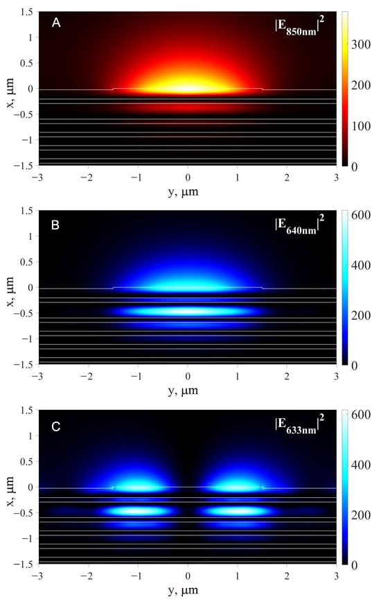
Figure 3.
Electric field intensity distribution for red-detuned attracting light beam, nm, (A), blue-detuned repulsive light beam, nm, (B) and auxiliary blue-detuned repulsive light beam for lateral support, nm, (C).
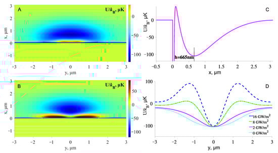
Figure 4.
Optical potential well when two wavelengths of 850 nm and 640 nm are involved (A), and when the third auxiliary wavelength of 633 nm is added (B). Vertical cross-section of the potential well at y = 0 (C) and horizontal cross-sections of the potential well at x = 665 nm for different intensities of the 633 nm wave (D).
The total potential of the atom near the surface is the sum of the optical potentials of all participating light beams and the Casimir–Polder potential together with the gravitational potential:
where J m3 is the van der Waals coefficient, nm is the reduced wavelength [18,50] describing the attractive interaction between atoms and the glass surface and m/s2 is the acceleration of free fall.
3. Results
3.1. Example of Specification of a 2D Waveguide Placed on a 1D PC
After selecting a waveguide height of 25 nm (above the last layer with a thickness of nm, see Figure 2), the width of the waveguide has to be selected. Both the semianalytical VEIM solver and the numerical FDE solver show that the waveguide with sustains single TE00 mode propagation for nm and nm with effective RI and , respectively. In addition, at wavelength nm, the TE01 mode with is also supported in the waveguide with width. The next (TE00) mode at nm has an effective index of . Therefore, only three modes with the electric field intensity distribution shown in Figure 3 are excited at excitation angles of . The third mode with nm is needed to provide ’lateral support’ for the ultracold atoms in the optical trap above the waveguide with width.
The calculated mode parameters for the rib waveguide with are presented in Table 2. Their effective RI, the fraction of Poynting energy transmitted through the vacuum, the effective area of the modes and the losses are given. The optical power in these modes required to form a 100 trap, as in Figure 4A–C, is also indicated. Note that in these waveguides, a significant fraction of the Poynting energy propagates through the external medium (vacuum). This is a unique property of the presented 1D PC waveguides that is unattainable for standard waveguides, where most of the Poynting energy is transmitted through the waveguide core and only a small fraction of the evanescent wave is available to manipulate atoms in the vacuum.
Table 2.
The calculated mode parameters for the rib waveguide with .
The mode losses were calculated assuming that the imaginary part of the RI of and is . According to [51], values as low as in this spectral range can be obtained for these dielectric materials using ion-assisted electron beam deposition. We set to account for scattering losses, which can be quite prominent for PC SMs with effective refractive indices close to unity.
3.2. Optical Trap above the Waveguide Located on the 1D PC
The total well trap potentials of the atom above the rib glass waveguide on 1D PC, which are calculated using the Equation (6), are shown in Figure 4. Figure 4A shows a potential with two wavelengths: attracting (red-detuned, nm) and repulsive (blue-detuned, nm). One can see in this figure a common problem for this type of potential: weak localization in the lateral dimensions and a decrease in the height of the well trap near the edge of the waveguide (i.e., near m in our case). In the vicinity of these points, atoms will escape from the trap. To solve this problem, the third beam with the wavelength of nm (TE01) is added, and the resulting total potential is shown in Figure 4B. That is, all the modes shown in Figure 3 are used in Figure 4B. It is clear that such ’lateral support’ dramatically improves lateral localization and eliminates atom escape paths to the surface through points m.
In Figure 4C, a vertical cross-section of the potential well at is shown. The minimum of the well is at nm from the surface. This should provide a very stable confinement of atoms at large distances from the dielectric surface, where the influence of the van der Waals force is negligible. The light intensities (see Table 2) are chosen so that the trap depth is 100 K. The sum of all light intensities gives the total atomic light scattering rate at the center of the trap, Hz by Equation (4).
The extent of the lateral localization can be easily controlled by varying the intensity of the nm (TE01) lightwave, as shown in Figure 4D, where cross-sections of the potential well at nm are shown. The dotted cyan line corresponds to the absence of the auxiliary lateral localization (i.e., this is the horizontal cross-section of Figure 4A). The solid magenta line is the horizontal cross-section of Figure 4B, while the other two lines show how the lateral confinement increases as the intensity of the TE01 auxiliary lightwave increases.
3.3. Techniques to Mitigate Temperature Rise Caused by Optical Absorption in Waveguides
Since the high intensity of the optical fields (used to trap the atoms) can potentially heat up and even damage the optical waveguides, possible ways to mitigate this problem should be mentioned. First, it should be noted that in waveguides on planar 1D PC, these problems are somewhat reduced by default, since the intensity maximum is near the interface and about half of the Poynting energy is transmitted through the vacuum. In a standard waveguide, only a small fraction of the total intensity is used to trap atoms, while the core of the waveguide is heated by the main part of the optical intensity.
A similar problem routinely arises in the context of the trapping of micrometer-sized particles in water by surface nanostructures using near-field optical tweezers [52,53,54,55]. There, even a moderate increase in the temperature of the nanostructures leads to convection of the water (in which the trapping takes place) and even to boiling, which prevents the trapping. To avoid this, several techniques have been proposed, including integrating a heat sink feature into the structure or using a substrate with high thermal conductivity. The same approaches can be used for the waveguide on planar 1D PC if optical absorption within the waveguide becomes an issue. The main problem with heat dissipation is the relatively low thermal conductivity of glasses and other transparent materials at room temperature, e.g., the thermal conductivity of pure fused silica is [56,57]. The use of sapphire ( [58]) as a substrate or indium tin oxide (ITO, [59]) as an integrating sublayer is one of the possible ways to distribute heat from the waveguide width in the lateral direction. Another way is to deposit gold films (∼250–300, depending on the film thickness [60]), parallel to the waveguide at a distance of about 10m from its left and right sides, where the waveguide lateral optical field vanishes.
In contrast to the experiments with optical tweezers in water, the allowable temperature rise in our case is much higher and is limited only by structural deformation and degradation of the glass waveguide. The typical glass transformation temperature is above 500 °C [61].
3.4. Excitation of Waveguide Modes in a Kretschmann-like Scheme
For the excitation of only two/three necessary modes and for avoiding the excitation of undesired additional modes (e.g., at nm on a flat surface; see Figure 2B, or at nm (TE00) in the rib waveguide), the Kretschmann-type scheme is quite convenient. In this scheme, mode excitation takes place via a coupling prism on which the optimal number of double layers N (see (2)) is deposited. For the presented photonic structure, this number for the optimal excitation is . With optimal excitation of a surface wave, there is no reflection of an incident beam due to destructive interference of the reflected wave with the optical surface wave reradiated back to the prism. Only modes with close to unity can be excited if the beam excitation angle (see Figure 1) is chosen near the total internal angle (i.e., near ). The prism coating can be arranged in such a way that half of the prism surface is covered by a PC structure (2) with (for excitation), while the other half has the same structure with (for propagation without reradiation back into the prism).
4. Discussion
Engineering the optimal interface for the light–atom interaction is critically important for developing compact and robust quantum sensors based on guided atom interferometers. In this communication, a novel waveguide structure based on planar 1D PC is presented, which is designed to trap and waveguide neutral atoms by optical dipole force. This photonic structure makes it possible to increase penetration depths of the evanescent light waves, which provides very stable trapping of atoms at relatively large distances from the dielectric surface of the waveguide. Additional stabilization of the atom in the lateral dimension by the auxiliary TE01 mode was also considered. By modulating the intensity of this mode, the lateral width of the well trap can be easily modulated, which can be used, e.g., for adiabatic cooling and other manipulations of ultracold atomic ensembles.
Funding
This research was funded by the Russian Science Foundation grant 22-22-00836.
Data Availability Statement
The data that support the findings of this study are available from the corresponding author upon reasonable request.
Acknowledgments
The author thanks Yuri B. Ovchinnikov for his lecture on cold atom waveguiding and the subsequent discussions that prompted the writing of this communication.
Conflicts of Interest
The author declares no conflict of interest.
References
- Bongs, K.; Bennett, S.; Lohmann, A. Quantum sensors will start a revolution—if we deploy them right. Nature 2023, 617, 672–675. [Google Scholar] [CrossRef]
- Bongs, K.; Holynski, M.; Vovrosh, J.; Bouyer, P.; Condon, G.; Rasel, E.; Schubert, C.; Schleich, W.P.; Roura, A. Taking atom interferometric quantum sensors from the laboratory to real-world applications. Nat. Rev. Phys. 2019, 1, 731–739. [Google Scholar]
- Cladé, P.; Guellati-Khélifa, S.; Schwob, C.; Nez, F.; Julien, L.; Biraben, F. A promising method for the measurement of the local acceleration of gravity using Bloch oscillations of ultracold atoms in a vertical standing wave. Europhys. Lett. 2005, 71, 730. [Google Scholar] [CrossRef]
- Ferrari, G.; Poli, N.; Sorrentino, F.; Tino, G. Long-lived Bloch oscillations with bosonic Sr atoms and application to gravity measurement at the micrometer scale. Phys. Rev. Lett. 2006, 97, 060402. [Google Scholar] [CrossRef]
- Tino, G.M. Testing gravity with cold atom interferometry: Results and prospects. Quantum Sci. Technol. 2021, 6, 024014. [Google Scholar]
- Bolotin, Y.; Golovan, A.; Vyazmin, V.; Evstifeev, M.; Vershovskii, A. Advanced gravity field survey methods. In Methods and Technologies for Measuring the Earth’s Gravity Field Parameters; Springer: Berlin/Heidelberg, Germany, 2022; pp. 237–301. [Google Scholar]
- Ge, G.; Chen, X.; Li, J.; Zhang, D.; He, M.; Wang, W.; Zhou, Y.; Zhong, J.; Tang, B.; Fang, J.; et al. Accuracy improvement of a compact 85Rb atom gravimeter by suppressing laser crosstalk and light shift. Sensors 2023, 23, 6115. [Google Scholar] [CrossRef]
- Mao, D.K.; Deng, X.B.; Luo, H.Q.; Xu, Y.Y.; Zhou, M.K.; Duan, X.C.; Hu, Z.K. A dual-magneto-optical-trap atom gravity gradiometer for determining the Newtonian gravitational constant. Rev. Sci. Instrum. 2021, 92, 053202. [Google Scholar]
- Dutta, I.; Savoie, D.; Fang, B.; Venon, B.; Alzar, C.G.; Geiger, R.; Landragin, A. Continuous cold-atom inertial sensor with 1 nrad/sec rotation stability. Phys. Rev. Lett. 2016, 116, 183003. [Google Scholar] [CrossRef]
- Garrido Alzar, C.L. Compact chip-scale guided cold atom gyrometers for inertial navigation: Enabling technologies and design study. AVS Quantum Sci. 2019, 1, 014702. [Google Scholar]
- Keil, M.; Amit, O.; Zhou, S.; Groswasser, D.; Japha, Y.; Folman, R. Fifteen years of cold matter on the atom chip: Promise, realizations, and prospects. J. Mod. Opt. 2016, 63, 1840–1885. [Google Scholar]
- McGilligan, J.P.; Moore, K.; Dellis, A.; Martinez, G.; de Clercq, E.; Griffin, P.; Arnold, A.; Riis, E.; Boudot, R.; Kitching, J. Laser cooling in a chip-scale platform. Appl. Phys. Lett. 2020, 117, 054001. [Google Scholar] [CrossRef]
- Li, D.; He, W.; Shi, S.; Wu, B.; Xiao, Y.; Lin, Q.; Li, L. Review of atom chips for absolute gravity sensors. Sensors 2023, 23, 5089. [Google Scholar]
- Ol’shanii, M.; Ovchinnikov, Y.B.; Letokhov, V. Laser guiding of atoms in a hollow optical fiber. Opt. Commun. 1993, 98, 77–79. [Google Scholar] [CrossRef]
- Barnett, A.; Smith, S.; Olshanii, M.; Johnson, K.; Adams, A.; Prentiss, M. Substrate-based atom waveguide using guided two-color evanescent light fields. Phys. Rev. A 2000, 61, 023608. [Google Scholar] [CrossRef]
- Burke Jr, J.P.; Chu, S.T.; Bryant, G.W.; Williams, C.J.; Julienne, P.S. Designing neutral-atom nanotraps with integrated optical waveguides. Phys. Rev. A 2002, 65, 043411. [Google Scholar]
- Ovchinnikov, Y.B.; Shul’ga, S.; Balykin, V. An atomic trap based on evanescent light waves. J. Phys. B At. Mol. Opt. Phys. 1991, 24, 3173. [Google Scholar] [CrossRef]
- Ovchinnikov, Y.B.; Ayi-Yovo, F.E. Towards all-optical atom chips based on optical waveguides. New J. Phys. 2020, 22, 053003. [Google Scholar] [CrossRef]
- Ovchinnikov, Y.B. A perspective on integrated atomo-photonic waveguide circuits. Appl. Phys. Lett. 2022, 120, 010502. [Google Scholar] [CrossRef]
- Konopsky, V. Design of 1D photonic crystals sustaining optical surface modes. Coatings 2022, 12, 1489. [Google Scholar] [CrossRef]
- Arnaud, J.A.; Saleh, A.A.M. Guidance of surface waves by multilayer coatings. Appl. Opt. 1974, 13, 2343–2345. [Google Scholar] [CrossRef]
- Yeh, P.; Yariv, A.; Hong, C.S. Electromagnetic propagation in periodic stratified media. I. General theory. J. Opt. Soc. Am. 1977, 67, 423–438. [Google Scholar] [CrossRef]
- Yeh, P.; Yariv, A.; Cho, A.Y. Optical surface waves in periodic layered media. Appl. Phys. Lett. 1978, 32, 104–105. [Google Scholar] [CrossRef]
- Robertson, W.M.; May, M.S. Surface electromagnetic waves on one-dimensional photonic band gap arrays. Appl. Phys. Lett. 1999, 74, 1800–1802. [Google Scholar] [CrossRef]
- Shinn, A.; Robertson, W. Surface plasmon-like sensor based on surface electromagnetic waves in a photonic band-gap material. Sens. Actuator B-Chem. 2005, 105, 360–364. [Google Scholar]
- Konopsky, V.N.; Alieva, E.V. Long-range propagation of plasmon polaritons in a thin metal film on a one-dimensional photonic crystal surface. Phys. Rev. Lett. 2006, 97, 253–904. [Google Scholar] [CrossRef]
- Hamidi, S.; Ramezani, R.; Bananej, A. Hydrogen gas sensor based on long-range surface plasmons in lossy palladium film placed on photonic crystal stack. Opt. Mater. 2016, 53, 201–208. [Google Scholar] [CrossRef]
- Ignatyeva, D.O.; Knyazev, G.A.; Kapralov, P.O.; Dietler, G.; Sekatskii, S.K.; Belotelov, V.I. Magneto-optical plasmonic heterostructure with ultranarrow resonance for sensing applications. Sci. Rep. 2016, 6, 28077. [Google Scholar] [CrossRef]
- Li, J.; Tang, T.; Zhang, Y.; Luo, L.; Sun, P. Magneto-plasmonic sensor with one dimensional photonic crystal for methane detection. Optik 2018, 155, 74–80. [Google Scholar] [CrossRef]
- Ignatyeva, D.; Kapralov, P.; Golovko, P.; Shilina, P.; Khramova, A.; Sekatskii, S.; Nur-E-Alam, M.; Alameh, K.; Vasiliev, M.; Kalish, A.; et al. Sensing of surface and bulk refractive index using magnetophotonic crystal with hybrid magneto-optical response. Sensors 2021, 21, 1984. [Google Scholar] [CrossRef]
- Konopsky, V.N.; Alieva, E.V. Photonic crystal surface waves for optical biosensors. Anal. Chem. 2007, 79, 4729–4735. [Google Scholar] [CrossRef]
- Guo, Y.; Ye, J.Y.; Divin, C.; Huang, B.; Thomas, T.P.; Baker, J.R., Jr.; Norris, T.B. Real-time biomolecular binding detection using a sensitive photonic crystal biosensor. Anal. Chem. 2010, 82, 5211–5218. [Google Scholar] [CrossRef] [PubMed]
- Konopsky, V.N.; Karakouz, T.; Alieva, E.V.; Vicario, C.; Sekatskii, S.K.; Dietler, G. Photonic crystal biosensor based on optical surface waves. Sensors 2013, 13, 2566–2578. [Google Scholar] [CrossRef] [PubMed]
- Rivolo, P.; Michelotti, F.; Frascella, F.; Digregorio, G.; Mandracci, P.; Dominici, L.; Giorgis, F.; Descrovi, E. Real time secondary antibody detection by means of silicon-based multilayers sustaining Bloch surface waves. Sens. Actuators B Chem. 2012, 161, 1046–1052. [Google Scholar] [CrossRef]
- Wei, C.; Cen, M.; Chui, H.C.; Cao, T. Numerical study of biosensor based on α-MoO3/Au hyperbolic metamaterial at visible frequencies. J. Phys. D Appl. Phys. 2020, 54, 034001. [Google Scholar] [CrossRef]
- Khodami, M.; Hirbodvash, Z.; Krupin, O.; Wong, W.R.; Lisicka-Skrzek, E.; Northfield, H.; Hahn, C.; Berini, P. Fabrication of Bloch long range surface plasmon waveguides integrating counter electrodes and microfluidic channels for multimodal biosensing. J. Microelectromech. Syst. 2021, 30, 686–695. [Google Scholar] [CrossRef]
- Kalas, B.; Ferencz, K.; Saftics, A.; Czigany, Z.; Fried, M.; Petrik, P. Bloch surface waves biosensing in the ultraviolet wavelength range – Bragg structure design for investigating protein adsorption by in situ Kretschmann-Raether ellipsometry. Appl. Surf. Sci. 2021, 536, 147869. [Google Scholar] [CrossRef]
- Delfan, A.; Liscidini, M.; Sipe, J.E. Surface enhanced Raman scattering in the presence of multilayer dielectric structures. JOSA B 2012, 29, 1863–1874. [Google Scholar] [CrossRef]
- Konopsky, V.N.; Alieva, E.V.; Alyatkin, S.Y.; Melnikov, A.A.; Chekalin, S.V.; Agranovich, V.M. Phase-matched third-harmonic generation via doubly resonant optical surface modes in 1D photonic crystals. LIght Sci. Appl. 2016, 5, e16168. [Google Scholar] [CrossRef][Green Version]
- Fong, N.R.; Menotti, M.; Lisicka-Skrzek, E.; Northfield, H.; Olivieri, A.; Tait, N.; Liscidini, M.; Berini, P. Bloch long-range surface plasmon polaritons on metal stripe waveguides on a multilayer substrate. ACS Photonics 2017, 4, 593–599. [Google Scholar] [CrossRef]
- Degli-Eredi, I.; Sipe, J.; Vermeulen, N. TE-polarized graphene modes sustained by photonic crystal structures. Opt. Lett. 2015, 40, 2076–2079. [Google Scholar] [CrossRef]
- Konopsky, V.; Prokhorov, V.; Lypenko, D.; Dmitriev, A.; Alieva, E.; Dietler, G.; Sekatskii, S. Electrical excitation of long-range surface plasmons in PC/OLED structure with two metal nanolayers. Nano-Micro Lett. 2020, 12, 1–8. [Google Scholar] [CrossRef] [PubMed]
- Kovalevich, T.; Belharet, D.; Robert, L.; Ulliac, G.; Kim, M.S.; Herzig, H.P.; Grosjean, T.; Bernal, M.P. Bloch surface waves at the telecommunication wavelength with lithium niobate as the top layer for integrated optics. Appl. Opt. 2019, 58, 1757–1762. [Google Scholar] [CrossRef] [PubMed]
- Konopsky, V. Version 1.1.8401.20377. 2022. Available online: https://www.pcbiosensors.com/1DPC4all.htm (accessed on 26 October 2023).
- Grimm, R.; Weidemüller, M.; Ovchinnikov, Y.B. Optical dipole traps for neutral atoms. In Advances in Atomic, Molecular, and Optical Physics; Elsevier: Amsterdam, The Netherlands, 2000; Volume 42, pp. 95–170. [Google Scholar]
- Ivanova, A.; Stoffer, R.; Hammer, M. A variational mode solver for optical waveguides based on quasi-analytical vectorial slab mode expansion. arXiv 2013, arXiv:1307.1315. [Google Scholar]
- Ivanova, O.; Hammer, M.; Stoffer, R.; Van Groesen, E. A variational mode expansion mode solver. Opt. Quantum Electron. 2007, 39, 849–864. [Google Scholar] [CrossRef]
- Zhu, Z.; Brown, T.G. Full-vectorial finite-difference analysis of microstructured optical fibers. Opt. Express 2002, 10, 853–864. [Google Scholar] [CrossRef]
- Miller, J.; Cline, R.; Heinzen, D. Far-off-resonance optical trapping of atoms. Physical Review A 1993, 47, R4567. [Google Scholar] [CrossRef]
- Thompson, J.D.; Tiecke, T.; de Leon, N.P.; Feist, J.; Akimov, A.; Gullans, M.; Zibrov, A.S.; Vuletić, V.; Lukin, M.D. Coupling a single trapped atom to a nanoscale optical cavity. Science 2013, 340, 1202–1205. [Google Scholar] [CrossRef]
- Sidqi, N.; Clark, C.; Buller, G.S.; Thalluri, G.K.V.; Mitrofanov, J.; Noblet, Y. Comparative study of dielectric coating materials for micro-cavity applications. Opt. Mater. Express 2019, 9, 3452–3468. [Google Scholar] [CrossRef]
- Wang, K.; Schonbrun, E.; Steinvurzel, P.; Crozier, K.B. Trapping and rotating nanoparticles using a plasmonic nano-tweezer with an integrated heat sink. Nat. Commun. 2011, 2, 469. [Google Scholar] [CrossRef]
- Lin, S.; Crozier, K.B. Trapping-assisted sensing of particles and proteins using on-chip optical microcavities. ACS Nano 2013, 7, 1725–1730. [Google Scholar] [CrossRef]
- Xu, Z.; Song, W.; Crozier, K.B. Optical trapping of nanoparticles using all-silicon nanoantennas. ACS Photonics 2018, 5, 4993–5001. [Google Scholar] [CrossRef]
- Brunetti, G.; Sasanelli, N.; Armenise, M.N.; Ciminelli, C. Nanoscale optical trapping by means of dielectric bowtie. Photonics 2022, 9, 425. [Google Scholar] [CrossRef]
- Sergeev, O.; Shashkov, A.; Umanskii, A. Thermophysical properties of quartz glass. J. Eng. Phys. 1982, 43, 1375–1383. [Google Scholar] [CrossRef]
- SCHOTT. Technical Information TIE-31: Mechanical and Thermal Properties of Optical Glass; SCHOTT: New York, NY, USA, 2004. [Google Scholar]
- Dobrovinskaya, E.R.; Lytvynov, L.A.; Pishchik, V. Properties of Sapphire. In Sapphire: Material, Manufacturing, Applications; Springer US: Boston, MA, USA, 2009; pp. 55–176. [Google Scholar]
- Thuau, D.; Koymen, I.; Cheung, R. A microstructure for thermal conductivity measurement of conductive thin films. Microelectron. Eng. 2011, 88, 2408–2412. [Google Scholar] [CrossRef]
- Lugo, J.; Oliva, A. Thermal properties of metallic films at room conditions by the heating slope. J. Thermophys. Heat Transf. 2016, 30, 452–460. [Google Scholar] [CrossRef]
- SCHOTT. Technical Information TIE-32: Thermal Loads on Optical Glass; SCHOTT: New York, NY, USA, 2004. [Google Scholar]


Disclaimer/Publisher’s Note: The statements, opinions and data contained in all publications are solely those of the individual author(s) and contributor(s) and not of MDPI and/or the editor(s). MDPI and/or the editor(s) disclaim responsibility for any injury to people or property resulting from any ideas, methods, instructions or products referred to in the content. |
© 2023 by the author. Licensee MDPI, Basel, Switzerland. This article is an open access article distributed under the terms and conditions of the Creative Commons Attribution (CC BY) license (https://creativecommons.org/licenses/by/4.0/).