1. Introduction
Silicon Carbide (SiC) represents a new challenge for detector manufacturing [
1]. The frontier activities of nuclear and subnuclear physics require devices with excellent performance in terms of stability and ability to operate at high fluxes of incident particles, e.g., for measuring cross-sections of very rare phenomena [
2]. SiC is extremely appealing for its expected features in terms of radiation hardness; it is a wide band gap semiconductor and is presently the most intensively studied because it is a good alternative to silicon as radiation hard device [
3,
4,
5,
6]. The irradiation is known to cause an appreciable deterioration of the detector performance [
7,
8]. Generally, the main evidence of damage is a fluence proportional increase of the leakage current. Loss of energy resolution and of charge collection efficiency are also signs of increasing damage. All these effects have been measured so far in an impressive number of systematic studies on Silicon [
9].
SiC p-n junctions should be potentially very robust devices from a radiation hardness point of view. Innovative detection systems construction for the new nuclear physics experiments at high beam luminosity, requires the development of large area devices able to survive the exposure of highest radiation levels. The requests of new and ambitious projects of the Italian National Institute of Nuclear Physics—INFN (NUMEN [
10], NuReLP [
11,
12,
13,
14]), led a cooperation between INFN and IMM-CNR, started in 2016, in order to develop a R&D activity on SiC technology. The SiCILIA project (Silicon Carbide detectors for Intense Luminosity Investigations and Applications) [
15] has been totally funded by INFN. Results on technological issues and particle detection applications have been recently published [
16,
17,
18].
In this work, we study the effects of damage in SiC from the point of view of both the electrical characteristics and the spectroscopic behavior as a nuclear particle detector. Radiation damage studies were conducted at the Laboratori Nazionali del Sud (INFN) in Catania, Italy, by using the ion beams delivered by the 15 MV Tandem accelerator in two different measurement sets. The Devices Under Test (DUTs) were mounted in the CT-2000 chamber, which is placed at the end of the 60-degree beam line. The chamber, with a diameter of 2 m, is equipped with 2 independently rotating arms to support detectors and with different collimation systems, allowing to measure precise angular distributions.
In a first experimental campaign, the DUTs were irradiated with 16O ions at 12.5 MeV, together with a standard silicon detector, for comparison. The DUTs were collimated so that just a small portion of the device was irradiated. In this way we have removed the effect of the different structure of the detectors, and only the effect of the different materials can be observed in this kind of experiment. To investigate the variation of the electrical characteristics properties as a function of the irradiation fluence, a second set of measurements was performed, with only the SiC detectors, in which we irradiated the whole device to verify its behavior under common operating conditions. Furthermore, due to the high radiation hardness of the SiC detectors observed in the previous experiment, it has been decided to use a heavier ion and the irradiation has been performed with 27Al.
The paper is organized as follows. After a brief recollection of the relevant SiC characteristics (
Section 2), the devices studied in this work are described in
Section 3. Results of the first measurement set, employing
16O for damaging the detectors, will be discussed in
Section 4.
Section 5 presents the results of the second set, where
27Al has been used. While
Section 4 and
Section 5 deal mostly with effects of radiation damage on the detection characteristics of SiC,
Section 6 presents a more detailed structural study of the behavior of the DUTs irradiated with
27Al: the produced defects are characterized using the Deep Level Transient Spectroscopy (DLTS) technique and changes in the current-voltage characteristics are also reported. The last section (
Section 7) is devoted to summarizing the work and drawing some conclusions.
2. Silicon Carbide Properties
SiC exists in more than 200 different polytypes, in which it can assume a wide variety of crystallographic structures (polytypism) depending on the stacking sequence of the atoms; the most common structures used for microelectronic applications are 3C [
19,
20], 4H and 6H [
21]. 4H-SiC is largely used in radiation hard applications [
22,
23,
24,
25].
Though the substrate material has recently improved both in size and purity, the present quality and uniformity of the epitaxial layers does not allow the processing of devices directly on it. Therefore, first of all, it is necessary to grow an epitaxial layer on a substrate that acts as the active region of the SiC detector. A seed substrate with very low defect concentration and the reduction of the density of defects present in the substrates by means of an epitaxial process allow a high-quality material to be obtained. The growth rate condition also has a significant influence on the defect formation or annihilation. Consequently, all these parameters are essential to obtain detectors with large area and thick active regions. Recently, due to the demands on the material quality and throughput increases, the chemical vapor deposition (CVD) as epitaxial growth technique was chosen. In the last decades, important progress on the epitaxial and hetero-epitaxial processes of silicon carbide has been made: introduction of chloride precursors [
26,
27], epitaxial growth on large area substrate with low defect density, improvement of the surface morphology, understanding of the CVD reactions and epitaxial mechanisms by advanced simulations [
28] point out the main results obtained in the homo-epitaxy process of 4H-SiC [
29]. Such evolution is a fundamental step towards the detectors manufacturing technology where large detection surfaces and thick devices are required.
Bulk damage is considered the limiting factor for the use of semiconductor detectors in the intense radiation field [
30]; hadrons or energetic leptons produce bulk damages primarily due to displacing a Primary Knock-on Atom (PKA) out of its lattice site. The process energy threshold, for several kinds of semiconductor materials, is reported in
Table 1; 4H-SiC epilayers exhibit an intermediate energy value in between Silicon and Diamond.
The pair of a Silicon (or Carbon) interstitial and a vacancy (denominated Frenkel pair) is a single displacement that can migrate through the lattice and may form point defects or agglomerate to form extended defects (particularly dislocations). The energy of a recoil PKA or residual atoms resulting from a nuclear reaction can be much higher. The energy loss along the paths of the recoils is due to two competing contributions: the collision with atomic electrons (collisional losses) and other displacements. Non-collisional interactions are predominant at the end of heavy recoil range and a dense agglomerate of defects (clusters) is formed. The bulk damage effects in semiconductor detectors are due to both the point defects along the incident particle paths and clusters at the end of the particles range. The detector performance is affected by point defects and clusters of point defects, depending on their concentration, energy level and the respective electron and hole capture cross-section. Defects that have deep energy levels in the middle of the forbidden gap could act as recombination/generation centers and to lead an increase of the reverse detector current. The effective doping concentration and the operating voltage needed to fully deplete the detector thickness change because of the generation of charged centers and the removal of dopants by formation of complex defects. These defects could also affect the carge collection efficiency by acting as trapping centers. In that respect the larger energy threshold to produce a PKA makes SiC a valid alternative to silicon.
Another advantage of SiC devices with respect to Silicon is the much smaller leakage current due essentially to the larger band gap [
31] (the reverse current density of SiC p-n junction is expected to be three order of magnitude smaller than for Si).
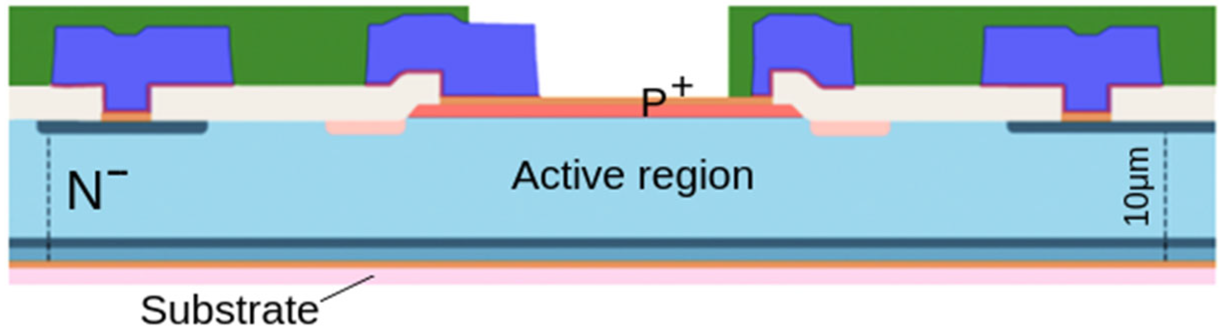
3. New Large Area p-n Junctions SiC Devices
The detectors studied in this work are new large area devices developed, during the SiCILIA project, by a collaboration between INFN, IMM and ST-Microelectronic. They are produced starting from 10–100 μm n
− epi-layers grown on 350 μm substrates. A cross section of the device is shown in
Figure 1. The first step of the processing is the growth of a double epitaxial layer, necessary for the p
+/n junction implementation. A p
+ layer 0.3–0.5 μm thick with an aluminum doping concentration of the order of 10
18–10
19/cm
3 is grown over the n
− epi-layer with a nitrogen doping concentration in the range 5–8 10
13/cm
3 (
Figure 1). After these phases, a first photolithography follows for the definition of the detector area by an ICP plasma etching and a second and a third lithography for the construction of the edge structure [
15]. This edge structure is needed to reduce the electric field at the device borders, and in particular, it is implemented by using a junction termination extension (JTE) by Al
+ implantation. Then, a third lithography is performed to realize by P
+ ion implantation a n
+ region on the edge of the device that acts as a field stop. After these two implants, a high temperature process at 1650 °C activates the dopants. The processing continues with the deposition of an isolation oxide and the opening of the contacts with a further photolithographic process. Then, the front metallization (Ni) is deposited and subsequently annealed to form a good ohmic contact on the p
+ and the n
+ region. The unreacted Ni on the oxide is then removed by a selective etch, and only on the periphery of the detector a thicker layer of Ti and Al is deposited for the bonding of the detector [
15]. After the lithography to define the metal layer, a thick polyamide layer is deposited for the passivation, and a further lithography is performed for the opening of the detector active area. Finally, the substrate is reduced from the backside by a mechanical process until a final thickness of the epitaxial layer plus the substrate of 110 μm, and the ohmic contact is formed by a titanium/nickel/gold deposited on the back of the wafer.
The active thickness of the devices tested in this work is about 10 μm. Then the depletion bias is about 4 V. The detector area is 5 × 5 mm2.
After the realization of the entire process, the detectors have been tested, cut off and mounted on a board for testing with ions.
4. Charge Collection Efficiency in SiC and Si When Damaged with 16O
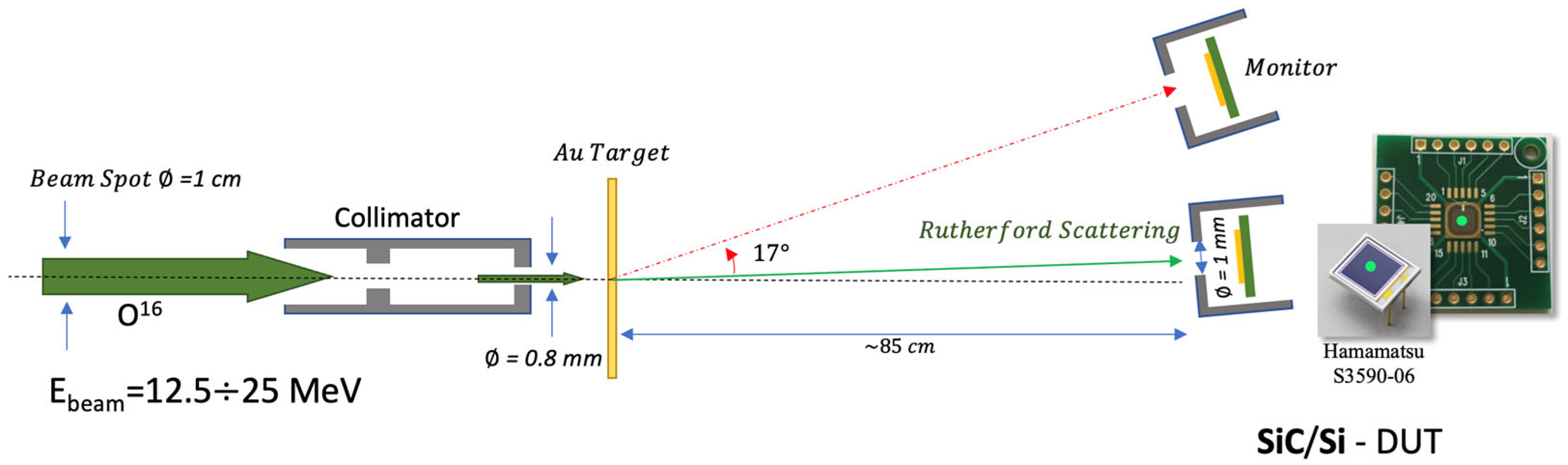
The effects of the irradiation on the performances of SiC when used as a spectroscopic detector are of particular interest for nuclear physics applications. In particular, in this section, we study the charge collection efficiency and the resolution degradation of the DUTs as a function of the ion fluence in the first measurement set performed by SiCILIA. In this set, the DUTs were placed in the CT-2000 vacuum chamber at about 85 cm from the target. A schematic view of the setup is shown in
Figure 2. The
197Au target is about 100 µg/cm
2 thick, placed normal to the beam direction. The beam energy is 12.5 MeV. The
16O beam is collimated to less than 1 mm before impinging on a
197Au target. The DUTs are placed at angles ranging from 0.5° to 10° with respect to the beam and collimated with a 1 mm diameter collimator to protect the edge structures from radiation damage effects. The ions enter the detectors from the junction (p
+) side. Each DUT is irradiated at a different fluence, ranging from 8.8 10
7 pp/cm
2 to 4.2 10
11 pp/cm
2, by placing the DUTs at different angles depending on the desired fluence. Different DUTs are used to evaluate the reproducibility of the results. In the same geometrical conditions, a silicon detector is irradiated at a larger energy (25 MeV) with the aim to compare the damage effects in the two different materials. In the first part of the study, the Tandem accelerator was set to deliver a high energy beam useful for the calibration of Si device; in such conditions, the radiation damage on Si detector was investigated. In the second part of the study, the energy of the
16O beam was reduced at 12.5 MeV to make the beam ions stop within the 10 μm of SiC and proceed with its investigation.
The SiC devices have been presented in
Section 3. The silicon detector used for comparison is an Hamamatsu S3590-06 p-i-n chip, 300 µm thick. Since the beam is stopped both in the SiC and in the Si detector, the larger thickness of the latter does not subtract from our conclusions in terms of radiation damage.
Standard spectroscopic electronics is used to process the signals: charge preamplifiers of 45 mV/MeV gain from the ASCOM company [
32], a spectroscopy amplifier (Mesytec Corporation mod. MSCF-16-F, Putzbrunn, Germany), set to 2 µs shaping time and a Silena 4418/V peak sensing ADC. The much larger capacitance of the SiC detector is associated with a larger electronic noise contribution to its energy resolution, with respect to the p-i-n silicon. However, electronic noise is not the dominant contribution to the energy resolution in our case.
The beam current is evaluated by using a pristine SiC detector used as a monitor and placed at 17° with respect to the beam direction (the beam current can be easily calculated from the detector active area and its counts per second, taking into account the Rutherford scattering cross section). From the beam current and the irradiation time, we evaluated the fluence for each DUT, again considering the Rutherford cross section at the corresponding polar angle. The fluence on the monitor detector is 103–105 times smaller than that on the DUTs, depending on the angle, so that the monitor does not experience any appreciable damage.
It is important to notice that, in this experiment, the Charge Collection Efficiency (CCE) is studied with the same ions producing the damage.
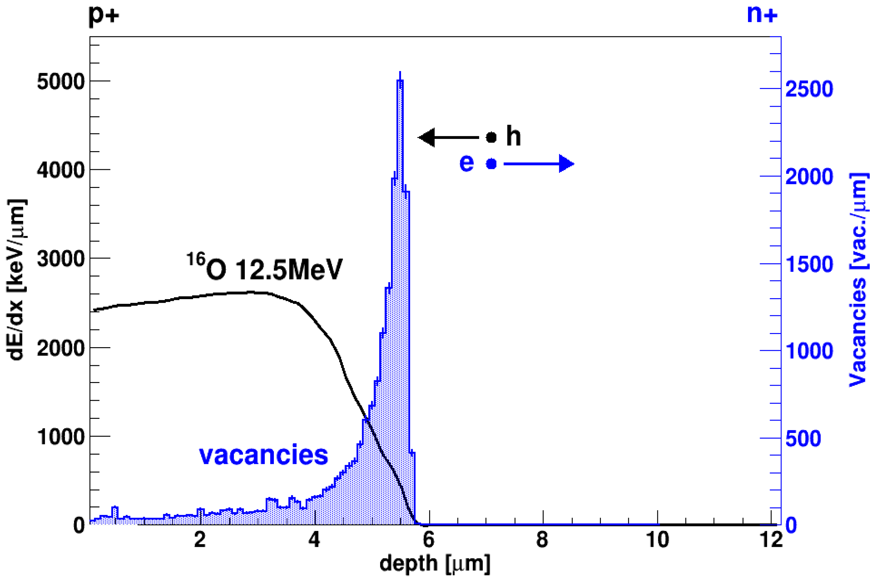
Figure 3 shows the distribution of the defects (vacancies) produced in SiC by a 12.5 MeV
16O ion, according to a SRIM [
33] simulation. Since the range of
16O ions in SiC is 5.6 µm, it is clear from the picture that most damage is produced at the very end of the ion range. The specific energy loss due to collisions with electrons is also reported (Bragg curve): the linear density of the electron-hole pairs produced by the ion is proportional to this value. After the ionization track is produced, electrons drift to the right, towards the n+ electrode; conversely, holes drift to the left, towards the p+ electrode. It is thus clear that electrons have to pass through the most damaged region in order to reach their collection electrode, after which they go through a relatively undamaged region. Holes, on the other end, drift all along the damaged region, though only part of them go through the most damaged zone.
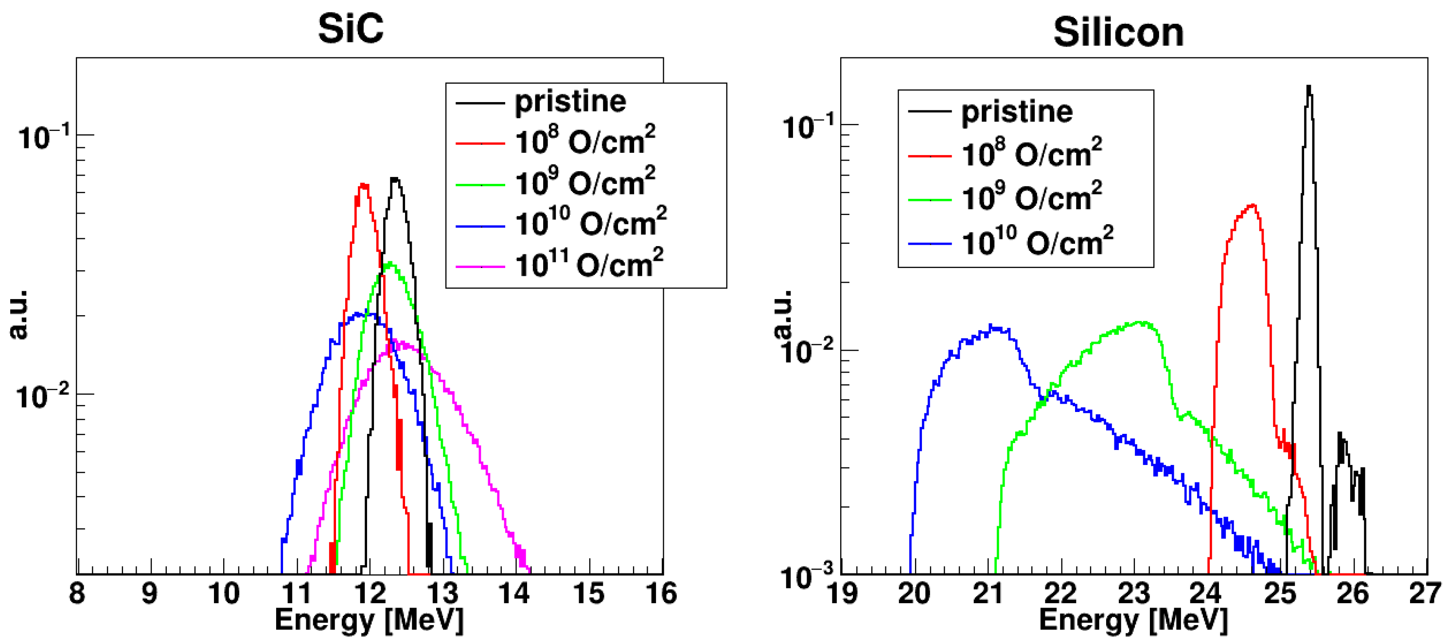
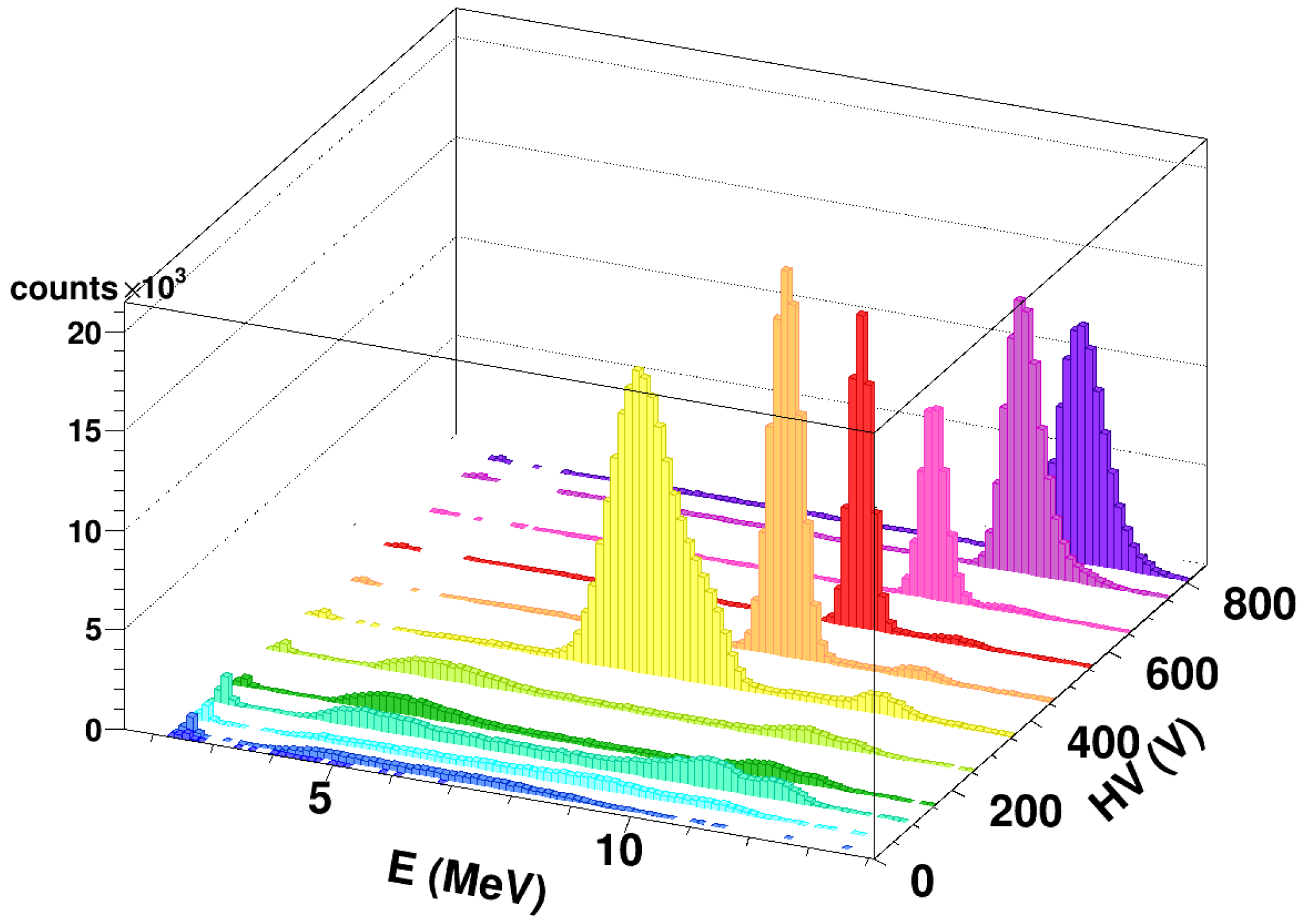
All detectors used for the investigation (Si and SiC) were preliminarily calibrated by using the
16O beam at different energies. Energy spectra of
16O beams for pristine and irradiated detectors are shown in
Figure 4 for different values of the ion fluence. Spectra are taken at the bias voltage corresponding to the maximum Charge Collection Efficiency (CCE) obtained. The left panel refers to a SiC detector, the right one to the Si detector. Since the impinging radiation is monoenergetic, the spectra are characterized by a single peak. For the SiC detector, the peak centroids are close to each other, since a CCE of about 100% is reached at all the fluences except 10
12 cm
−2. However, the peaks get larger for increasing fluence, showing increasing fluctuations in the charge collection process. As a matter of fact, in an actual nuclear physics experiment, a constant CCE is of great advantage, since the same energy calibration could be applied to all the acquired data. It is evident, from
Figure 4, that a constant CCE could be obtained for SiC, by suitably adapting the bias voltage, and not for silicon.
For silicon, the peak moves to a lower abscissa (i.e., we observe a reduction of the CCE) for increasing fluence, and already at 109 ions/cm2, it develops a tail on the right side and a shoulder on the left side, becoming asymmetric. Beyond 1010 ions/cm2, the detector stops working at all. Furthermore, the leakage current of the silicon detector increases considerably (from 0.2 μA up to 2 μA), even after the lowest dose value.
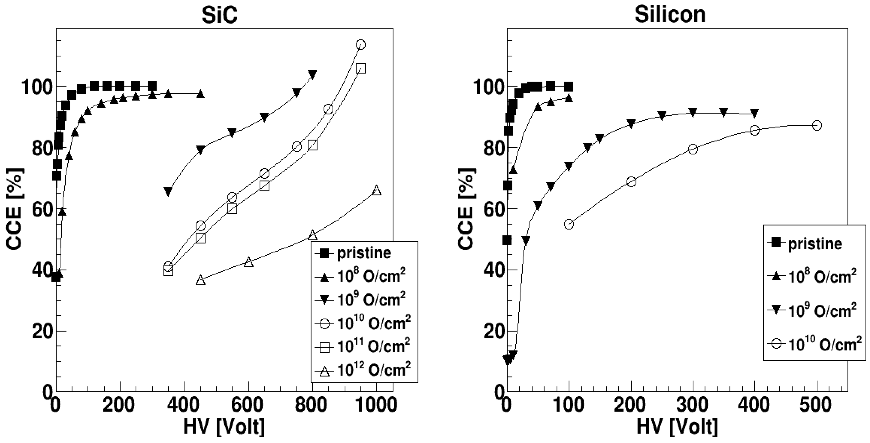
By studying the CCE of the SiC detector as a function of the applied voltage, one can notice that, starting at 10
9 cm
−2 fluence, a voltage of at least 300 V is needed to get a peak in the amplitude distribution. This behavior can be easily seen in
Figure 5, which shows the obtained spectra for the different applied voltages at a 10
9 cm
−2 fluence, and it is not due to a slowed down collection time, which could produce ballistic deficit in the amplitude measurement: the rise-time of the preamplifier signal is much shorter than the shaping time for all applied voltages. Though the reason for this effect is still under study, the large reduction of CCE at low reverse bias could be due to the setting of the experiment. In fact, part of the detector has been damaged at high fluence with oxygen ions, and just after a few minutes, the CCE has been measured with the same ions. With this procedure, even the transient defects that have a very low activation energy as reported in several previous papers [
34,
35,
36], can affect the CCE. During the CCE measurements, the annealing at room temperature produces a considerable reduction of the low activation energy traps, and then, a considerable increase of the CCE can be observed. A preliminary characterization with alpha sources has shown that, already a few days after irradiation, the CCE had substantially improved. Further studies are currently planned to quantify the effect.
Figure 6 shows the obtained CCE values as a function of the applied voltage. The CCE has been calculated only for those voltage values for which a proper peak is present. The most striking difference between the SiC and the silicon data is the behavior at the largest fluence values. The silicon detector always shows a tendency to saturate with increasing voltage. For increasing fluence, we can observe both a reduction of the CCE and an increase of the bias to obtain the saturation value: already at 10
8 cm
−2 the saturation value stays well below 100%.
The SiC detector, instead, shows an increasing CCE value, which even trespasses 100% at very high reverse bias (V > 800 V). This could be due to damage in the SiC material that produces a substantial change in the local doping concentration and, consequently, a peak of the electric field close to the electrodes and an impact ionization of the carriers in those regions. The impact ionization multiplication then gives a larger than 100% CCE, as already recognized in silicon detectors [
37]. As can be seen in
Figure 4, larger fluctuations are obtained at the largest fluences: This could be also due to the additional multiplication associated to the impact multiplication process. As a matter of fact, for the same fluences, the width of the distribution drastically decreases at lower bias voltages (associated to lower CCE values). This is also illustrated in
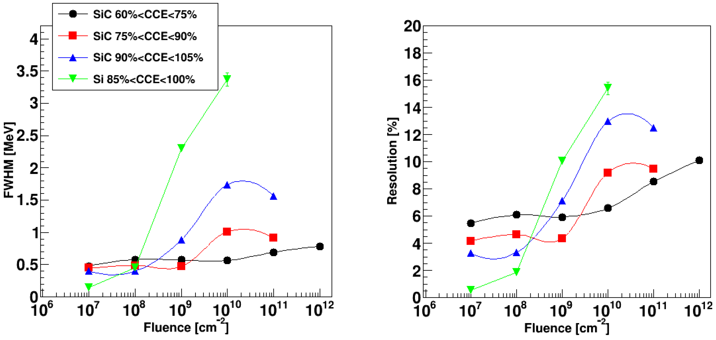
Figure 7, where the FWHM of the distribution (left panel) and the associated resolution (right panel) are reported as a function of the fluence.
The data for SiC are also shown for different CCE intervals, while data for silicon refer to the largest CCE value. Data for SiC extend to fluence values one or two orders of magnitude larger than for silicon since the SiC still produces a single peak at those fluences. It is also clear that the worsening of the performance, in terms of FWHM and resolution, is much steeper for silicon than for SiC, though the initial resolution of the silicon detector is better. The SiC points at CCE~100% show a much worse resolution than for lower CCE values. This could be due to the already mentioned impact ionization effect at large bias voltage. As a matter of fact, the SiC energy resolution stays below 10% even at a 1012 cm−2 fluence, provided that the bias voltage is not increased too much.
5. Charge Collection Efficiency and Resolution in SiC Damaged by 26Al
In the second measurement set, for irradiation with
27Al at 24.2 MeV, three DUTs were placed in the target position at 90° with respect to the beam direction. At this energy,
27Al has a range of 6.9 µm in SiC, and it is therefore stopped in the active region. The beam was purposely defocused to irradiate the whole surface as uniformly as possible. The DUTs, nominally identical, were irradiated at different fluences, ranging from 10
9 to 10
11 pp/cm
2. Before and after irradiation, each device was tested in vacuum, in terms of its spectroscopic performance, using two alpha sources: a
148Gd source (E = 3.183 MeV) and an
241Am source (main peak E = 5.486 MeV). The energy spectra were acquired with a standard spectroscopic electronic chain composed by a charge preamplifier of 45 mV/MeV gain from the ASCOM company [
32], a spectroscopy amplifier (ORTEC mod. 572), set to 2 µs shaping time, and a multi-channel analyzer. Differently from the experiment described in
Section 4, in the present measurement, the ion used to damage the detectors is not the same as that employed to characterize them. Moreover, the CCE was evaluated many hours after irradiation.
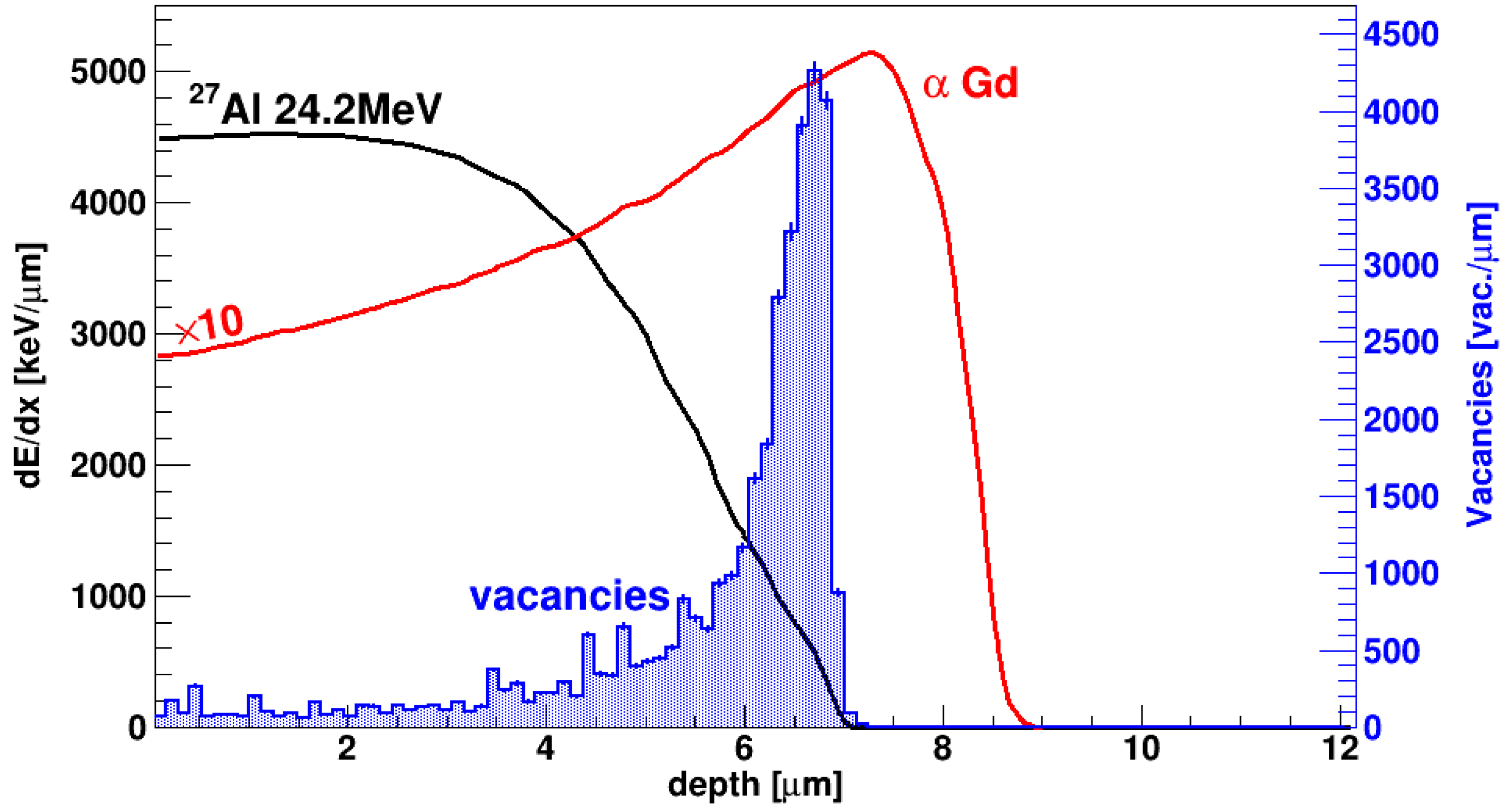
Figure 8 shows the distribution of the vacancies produced by the
27Al ions, together with their ionization profile and the one of the alphas from the
148Gd source. It is apparent, from
Figure 8, that for alpha particles the maximum density of the produced electron-hole pairs roughly corresponds to the maximum defect density.
The energy spectra of the 148Gd alpha source feature two peaks, one centered at 3.18 MeV and one centered at about 2.5 MeV. The former, relatively narrow, is associated with alpha particles impinging on the active area of the detector, where the only entrance window is due to the p+ electrode. The latter, much larger and slightly asymmetric, is due to alpha particles impinging closer to the borders of the active area, where a relatively thick passivation (7 µm of polyamide) is present: the alpha particles experience an energy loss of 0.6–0.8 MeV in the passivation layer before entering the active area. The data presented in this paper were obtained using only the “clean” peak not affected by the passivation.
The energy spectra have been calibrated for DUTs in pristine conditions, also using an 241Am alpha source. The alpha particles from the 241Am source, having a range of about 18 µm in SiC, are not stopped in the active region of the SiC detectors. Using both sources and both peaks (the “clean” peak and the one due to the passivation layer), we have developed a self-consistent calibration procedure, based on energy loss calculations. The procedure gives the calibration parameters for each spectrum and estimates the average dead layer thickness (about 2 µm SiC equivalent) and the active region thickness, the latter resulting slightly larger (12–13 µm) than the nominal value of 10 µm.
An analysis of the CCE has been performed for both alpha sources, and data obtained with the two sources are compatible.
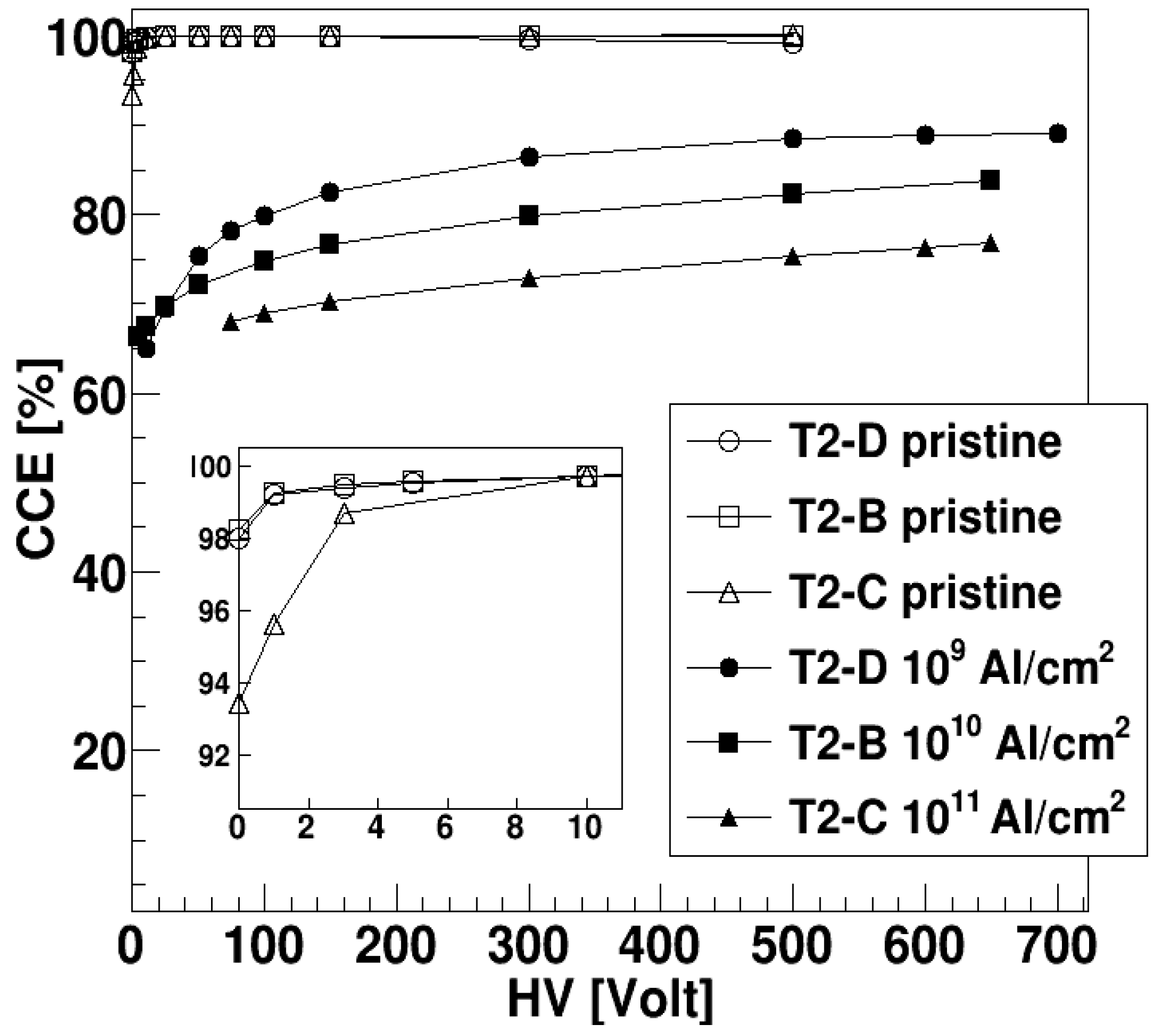
Figure 9 shows the CCE obtained using the
148Gd source, as a function of the applied voltage. The CCE is calculated from the centroid of the “clean” alpha peak, in energy units, normalized to the maximum centroid obtained for the pristine detector. All the DUTs have practically the same behavior before irradiation with the CCE reaching 100% already at 10 V bias voltage (see the inset in
Figure 10 where the values at low voltages for the pristine detectors are shown). The CCE decreases for increasing fluence. The bias voltage for which CCE saturates also tends to increase. This effect could be due to the decrease of the carrier lifetime produced by the damage in the silicon carbide epitaxial layer after the irradiation. For a given electric field, the carrier transit time is fixed, so that a decrease in the carrier lifetime produces a decrease of the CCE. By increasing the electric field, the transit time in the depletion layer is reduced so that a larger fraction of the charge can be collected. Even at the largest fluence (about 10
11 cm
−2), the CCE is reduced just by about 30%. Though a larger bias voltage is needed to saturate the CCE, after irradiation, the saturation value is already reached, within a few percent, at about 300 V. CCE is never larger than 100%, at variance with
Figure 6, but in this case the measurements have been done after several days (so that some annealing could have occurred) and with a different ion and energy with respect to those used for irradiation.
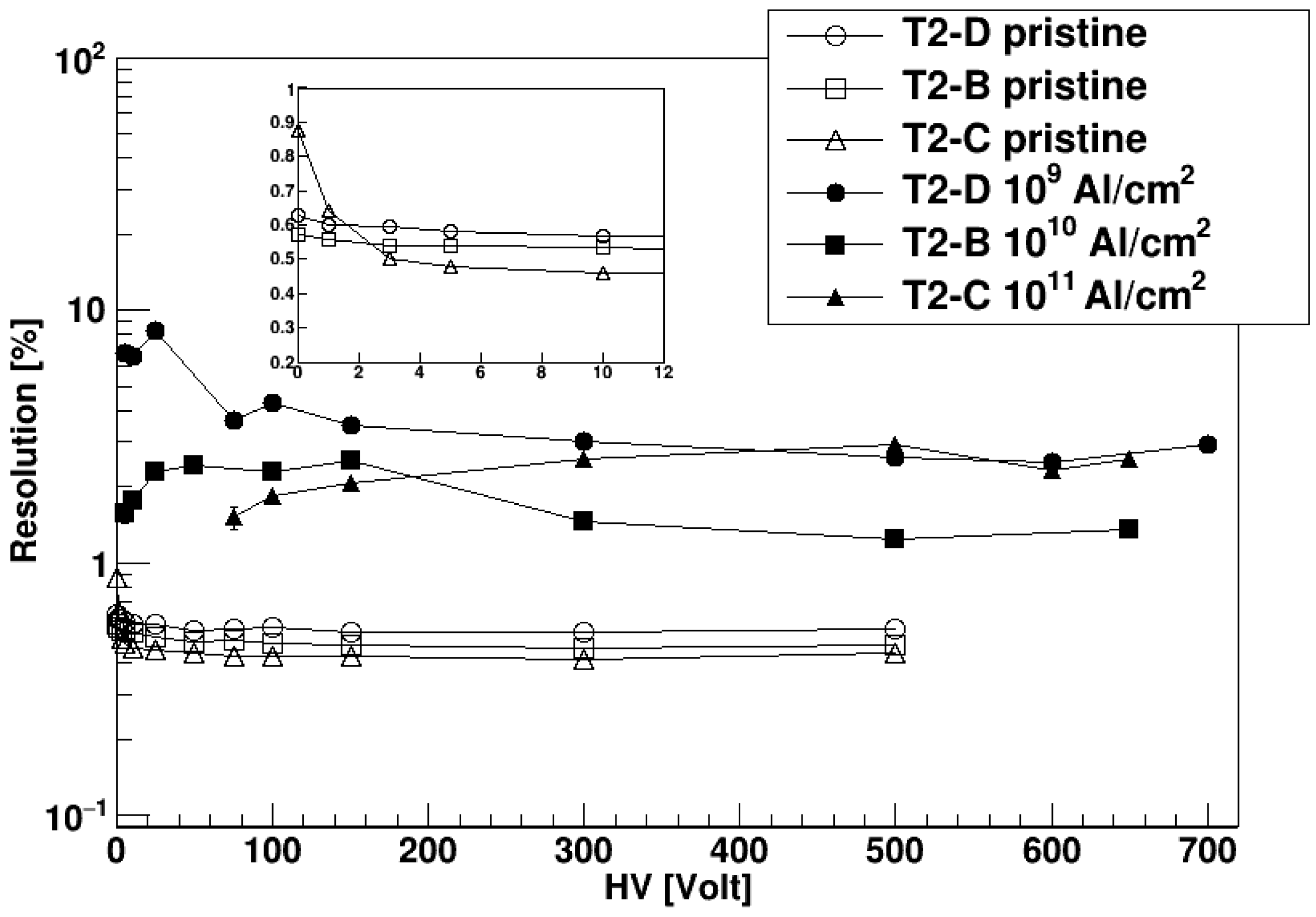
The shape of the alpha peaks has been found symmetric and Gaussian also after irradiation. Both the Full Width at Half Maximum (FWHM) of the peak and its centroid get smaller after irradiation. Their ratio, i.e., the energy resolution, is the parameter of interest when one wants to measure an unknown energy spectra. In
Figure 10 we report the resolution of the
148Gd alpha peak as a function of the bias voltage, for the three DUTs both before and after irradiation. Pristine detectors have very similar resolutions of ~0.5%. After irradiation, the resolution worsens by almost a factor of 10, reaching a few percent, a value in any case still acceptable in many of the foreseen applications. The fact that resolution values at 10
9 cm
−2 and 10
11 cm
−2 fluence are similar and larger than the value at 10
10 cm
−2 has come as a surprise, and it is still under study. The resolution is also only mildly dependent on the bias voltage, at least above ~50 V, and reaches a steady value already at 300 V.
6. DUTs Irradiated with 27Al: Electrical Characterization
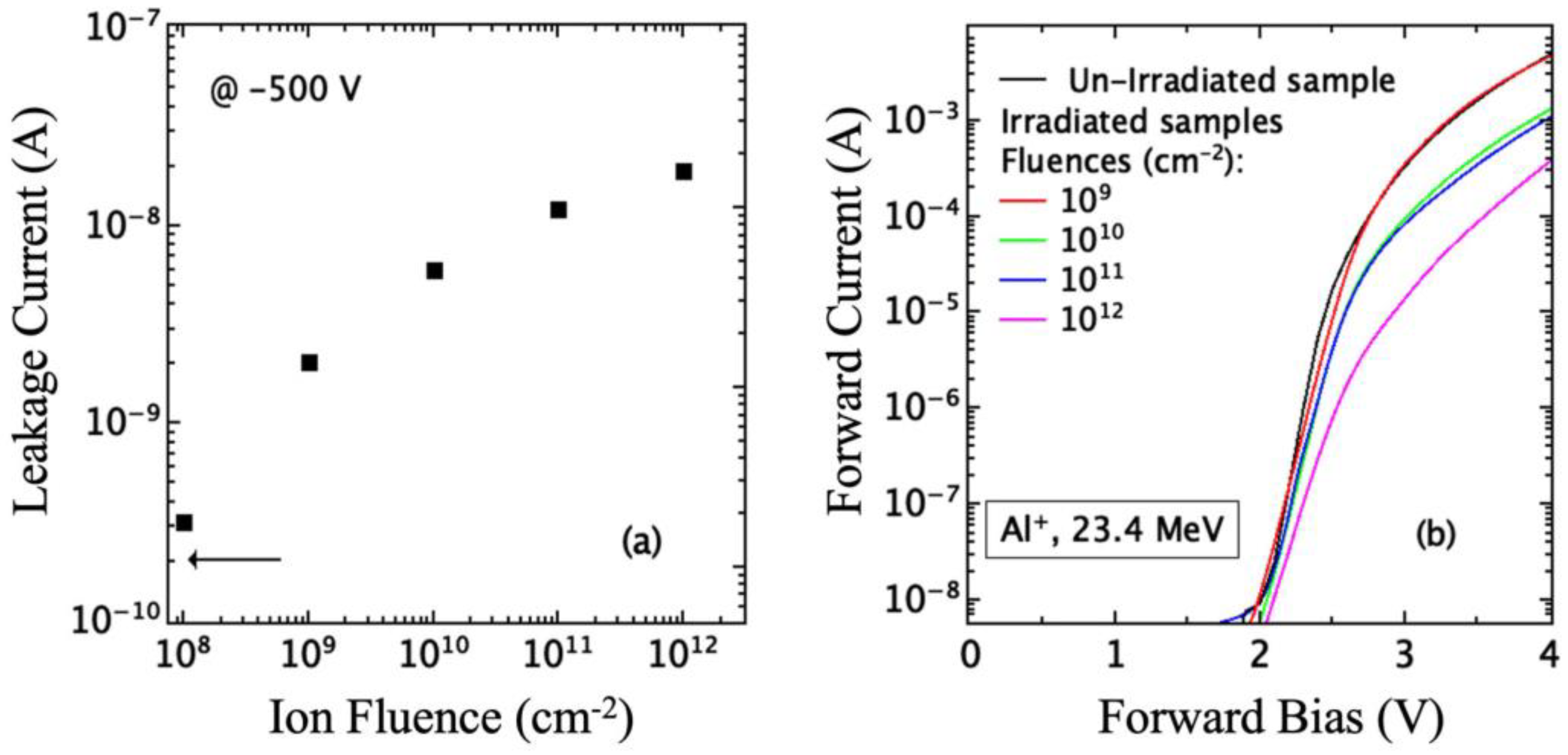
The forward and reverse I–V characteristics of the p-n junction have been measured before and after irradiation with 24.2 MeV Al ions at different fluences. The current–voltage measurement has been performed with the Keithley 6517 electrometer, Beaverton, OR, USA, which works as voltage source and as amperometer. The system has been interfaced to a PC through a GPIB interface. The reverse current measured at a bias of −500 V is reported in
Figure 11a versus the ion fluence: In the unirradiated diode it is about 3 × 10
−10 A (arrow in
Figure 11a) and increases after irradiation reaching a value of 2 × 10
−8 A at a fluence of 10
12 ions/cm
2. A similar effect was observed in Schottky diodes irradiated with 1.0 MeV Si [
5], and it was associated with the defects produced by irradiation.
As shown in
Figure 8, the energy loss and the vacancy concentration of 24.2 MeV Al ions, as calculated by SRIM simulator [
33], are not uniform in the device active layer as the ion range (6.6 μm) is lower than the epilayer thickness (10 μm). The primary vacancy concentration at the end of the ion range is about a factor ten higher than in the first 5 μm, as shown in
Figure 8. Then, in the first region of irradiated epilayer, only point defects (vacancy and interstitial) are produced instead around the ion range cluster of defects formed at least at high fluence [
38].
We have measured the I–V forward characteristics of the p-n junction before and after irradiation, and in
Figure 11b, the obtained results are reported. The unirradiated diode exhibits the typical behavior of a p-n junction, showing a turn-on voltage of about 1.8 V, an exponential increase of current with bias at low voltage and a linear increase at higher voltages (>2.5 V) due to presence of the series resistance [
39]. After irradiation, these characteristics change resulting in a decrease of the current at fixed bias and a right shift of characteristic: the knee shifts at higher bias and the diode turn-on voltage changes from about 1.8 V to about 2.2 V after irradiation.
In the low voltage region, this characteristic can be described with the Shockley-Hall-Read (SHR) generation current and with the model reported by C.T. Sah et al. [
40]. The current is related to the recombination in the space–charge region through deep levels near the middle of the bandgap. In that region, the current density can is given by:
where V is the applied bias,
n the ideality factor, K
B the Boltzmann constant, q the electron charge and T the absolute temperature. The pre-exponential factor J
0 in the relation (1) is obtained by the relation:
where w is the width of the recombination region, n
i the concentration of intrinsic charge carriers and τ
0 the carrier lifetime. However, the last parameter, τ
0, is given by the well-known relation [
31]:
where
Nt is the concentration of traps, σ the scattering cross section and
v the carrier velocity.
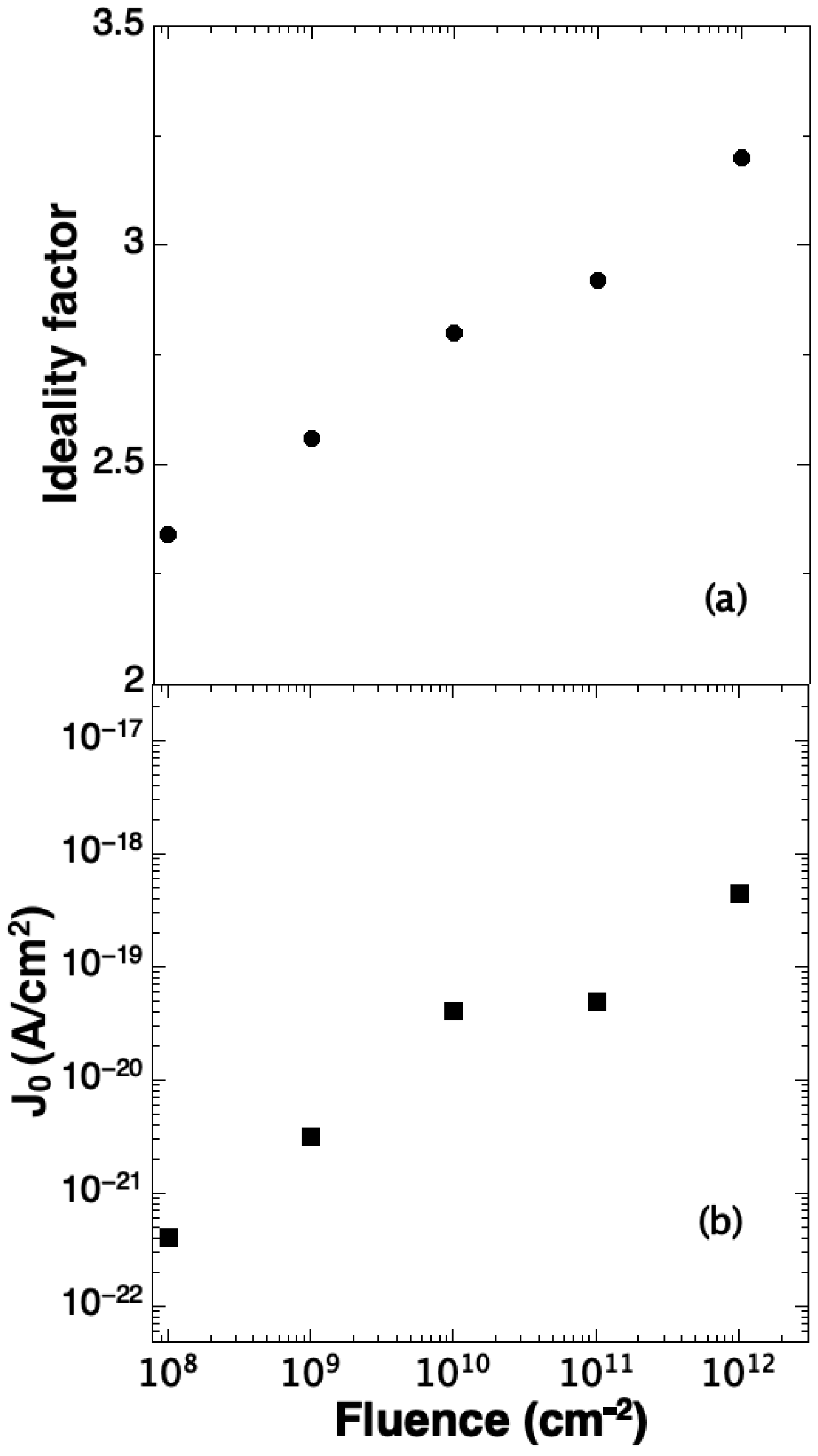
The obtained values of
n, calculated by Equation (1) in the bias range where exponential trend holds, are reported in
Figure 12a vs. the irradiation fluence. This parameter is about 2.3 in the unirradiated diode and increases with fluence reaching the value
n = 3.2 in the highest fluence irradiated diode. Pezzimenti et al. [
39] shows that the presence of defects considerably increases the ideality factor, and that, when the defect concentration becomes higher than 10
15 cm
−3, the value of the ideality factor increases and can reach values close to 3.0, typical of leaky diodes.
From the I–V curves, we have extracted the pre-exponential
J0 parameters. The obtained values are reported in
Figure 12b vs. the irradiation fluence: it is 4 × 10
−22 A/cm
2 in the unirradiated diode and increases to 5 × 10
−19 A/cm
2 in the highest fluence irradiated device. From Equation (2), we deduce that the change in J
0 can be associated to a change in the change of in
w and
τ0, as it is improbable any change of n
i.
Moreover, as reported in the literature [
38,
41], the change of w, can be extracted from the barrier capacitance C
0 (capacitance at V = 0) of the p-n junction. The maximum change of this parameter, as will be shown later, is of about a factor 3.5, then an increase of w of the same factor can be assumed. All these observations indicate that the measured increase of J
0 of more than three orders of magnitude is related to the decrease of the carrier lifetime
τ0 and then to the increase of defects concentration. This behavior has been confirmed by DLTS measurements, which will be presented in the following. Some authors of the present paper obtained similar results after irradiation of p-n junction with 600 Kev He ions [
38].
At high voltage, the forward I–V characteristics (
Figure 11b) tend to become flat as the effect of series resistance becomes dominant [
39]. All the characteristics show a similar trend, with a decrease of current for the same bias value when the irradiation fluence increases. This effect is ascribed to the rise of diode series resistance (R
s), and it was also observed in irradiated p-n junctions [
21,
22,
38] and Schottky diodes [
5,
42] and was associated to the defects created by irradiation.
In fact, the created defects exhibit acceptor-like behavior [
21,
43], then compensation effects occur with a decrease of carrier concentration and an increase of resistivity.
The overall diode series resistance (Rs) was extracted from the slope of the forward I–V curves in the high voltage region in the range 7.0 ÷ 8.0 V (not shown). The calculated values of Rs range from 1.5 Ohm for the unirradiated diodes to 5.8 Ohm for the highest fluence 1012 ions/cm2 irradiated device.
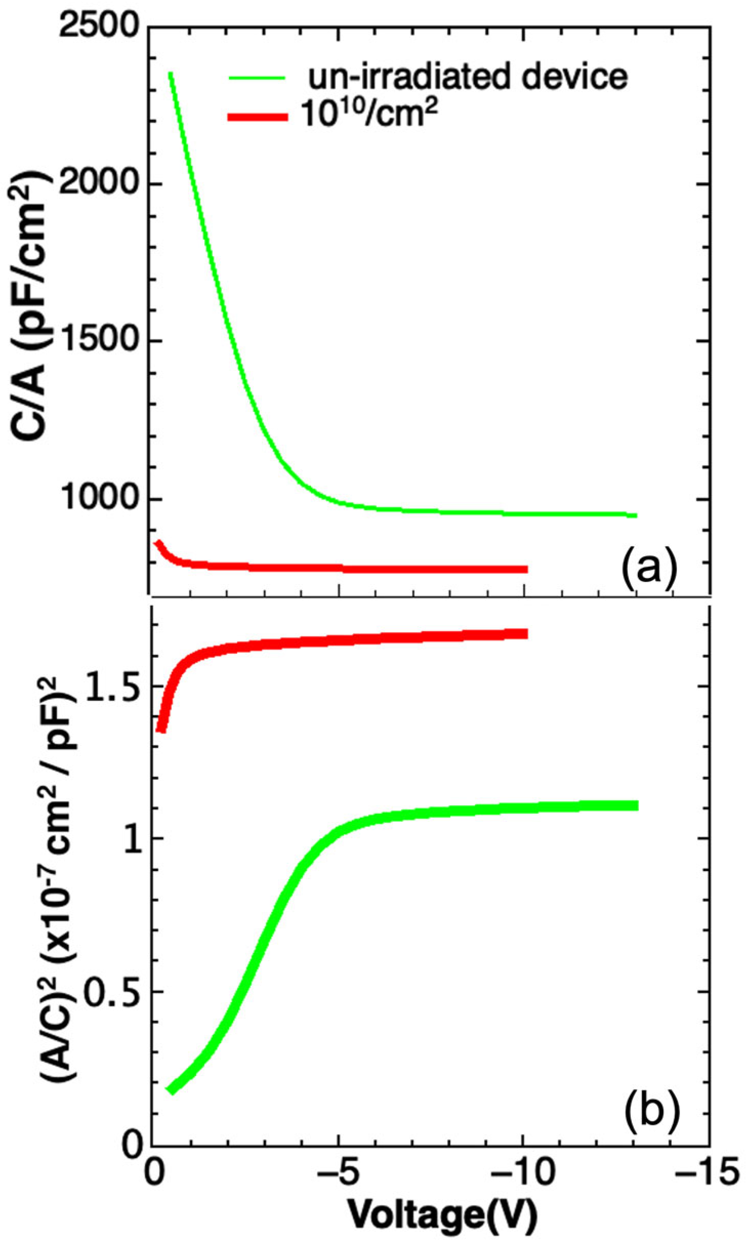
To evidence the occurrence of change in the carrier concentration, C-V measurements were performed on unirradiated and on some irradiated devices. The C-V curves of unirradiated diode and of a device irradiated with 24.2 MeV
27Al ions at a fluence of 10
10 Al/cm
2 are reported in
Figure 13.
Typical trends of C-V are observed in the unirradiated and irradiated detectors (
Figure 13a) and the value of carrier concentration (N
D-N
A), extracted from the (A/C)
2-V curves [
31] (
Figure 13b), is 9.5 × 10
13 cm
−3, very close to the nominal dopant concentration value- 8 × 10
13 cm
−3. After irradiation with 24.2 MeV
27Al ions at a fluence of 10
10 Al/cm
2 a change of C-V is observed (
Figure 13a): The capacitance decreases, and a different trend was observed at a lower bias (2.0 V) with respect to unirradiated diode (4.0 V), indicating that for this bias all the n-type layer is already depleted. The carrier concentration calculated from the corresponding (A/C)
2-V curve reported in
Figure 13b is 3.1 × 10
13 cm
−3, a factor three lower than in the unirradiated sample.
C-V measurements performed in devices irradiated at high fluence show that the capacitance depends much less on the applied voltage, probably due to the complete depletion of the n− region already at zero bias. Almost certainly at high fluence irradiation the carrier concentration could continue to decrease, and simultaneously, the mobility could be significantly reduced.
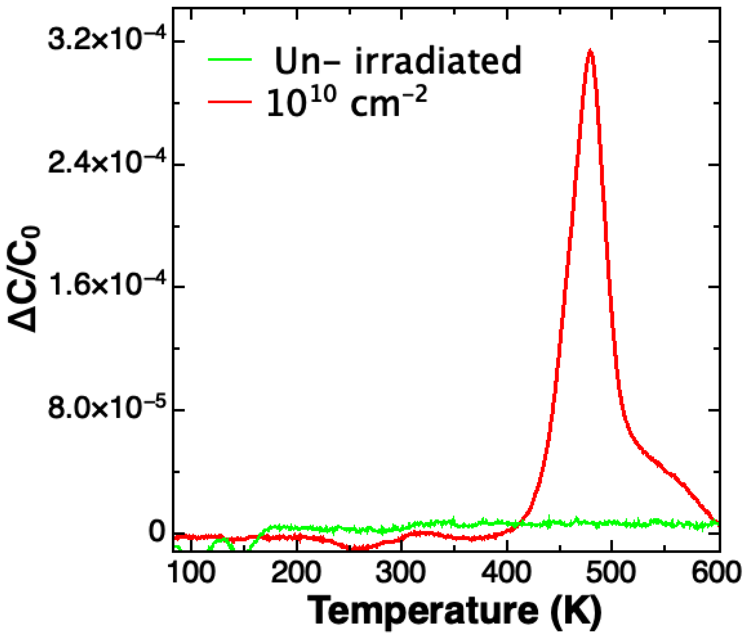
The changes of the pre-exponential parameter J0 and of the series resistance (or epilayer resistivity) are certainly both related to deep levels associated with defects generated in the material by irradiation. To investigate that, DLTS measurements were carried out in the device irradiated with 24.2 MeV 27Al at a fluence of 1010 ions/cm2.
SULA double boxcar spectrometer was used for DLTS measurements. The spectra were acquired in the temperature range 100–750 K by using rate windows in the range 2–200 s
−1. In
Figure 14 we report the obtained spectra measured in unirradiated and in 10
10 Al/cm
2 irradiated device.
The spectrum of unirradiated diode does not show any peaks, indicating the low concentration of processing defects. A main peak at 480 K with a broad band appears in the DLTS spectrum after irradiation at 1.0 × 10
10 ions/cm
2. The energy associated with the peak, determined by the Arrhenius plot obtained by performing measurements at different rate windows, is about 1.0 ± 0.05 eV below the conduction band. The concentration of this trap is about 10
10 traps/cm
3. Literature works relate these peaks (called RD
1/2) to radiation damage: Their energies are in the range 0.9–1.0 eV [
44,
45].
Regarding the microstructure of the defect associated with this trap, the exact correlation with a specific structural defect has not been yet established, but a V
Si or an antisite could be responsible for these centers [
43,
45].
The DLTS spectra agree with the trend of the J
0 parameter versus the irradiation fluence shown in
Figure 11: The increase of J
0 with fluence is to be imputed to the accumulation of point defects.
7. Summary
In this work we have reported an extended study on the radiation damage of SiC detectors.
In the first part, a comparison between the radiation damage of Si and SiC detectors has been performed. The detectors have been irradiated with 16O ions, stopped into the active area, and the same ions have been used for CCE evaluation (right after irradiation). While the CCE is similar between the two detectors, the resolution of the silicon detector deteriorates even at very low irradiation fluences (109 ions/cm2). The silicon detector signal shows a very asymmetric peak. The silicon carbide detector instead shows a small increase of the resolution even at larger fluences (1013 ions/cm2), and the signal is always symmetric.
In the second part of the experiment, a heavier ion (27Al instead of 16O) was used to test the SiC detectors at higher radiation damage, and even in this case, the signal was symmetric at high irradiation fluences. The CCE has been evaluated many hours after irradiation by exploiting a 148Gd alpha source. Without collimation a second signal appears due to the edge structure of the detector and the CCE is always larger than 70% even for the higher fluence of 1011 ions/cm2. The CCE is also always increasing with the increase of the bias of the detector, and no saturation is observed until 700 V.
The same detectors irradiated with 27Al have been characterized by I–V, C-V and DLTS. It has been observed that the radiation damage produces an increase of the point defects observed by DLTS (RD1/2), and this defect induces both an increase of the leakage current of the detector, a shift of the forward characteristics and a reduction of the CCE of the detector. Furthermore, even an increase of the ideality factor and a decrease of the doping concentration of the epitaxial layer has been observed at high irradiation fluences.
Even if the electrical measurements show an increase of the leakage current due to the formation of point defects, the detector parameters (CCE and resolution) in SiC detectors are still good, showing a much higher radiation hardness with respect to silicon.


 ,
, 


