1. Introduction
Metal oxides have gained significant attention in recent years as promising gas sensor materials. This is primarily due to their advantageous characteristics, including low cost, convenient processing, and high sensitivity [
1]. Metal oxide semiconductor gas sensors offer a range of benefits such as high sensitivity, significant signal output changes even in response to low concentration gases, long lifespan, rapid response rate, and excellent reversibility. These gas-sensing devices operate based on the principle of gas molecules interacting with the metal oxide, resulting in conductivity changes. Their unique advantages, such as high sensitivity, cost-effectiveness, ease of manufacturing, and compatibility with silicon microfabrication, have made them the focus of extensive research [
1,
2,
3]. Although zinc oxide (ZnO) thin films are widely employed in gas sensors, their effectiveness is constrained by their limited surface-to-volume ratios. Moreover, these sensors usually demand high operating temperatures exceeding 300 °C. Nevertheless, ZnO remains one of the most extensively researched gas sensing oxides due to its capability to detect a range of combustible and toxic gases. Notably, it has been studied extensively for the detection of gases such as NO
2 [
4,
5], C
2H
5OH [
5], CO [
6], and H
2 [
7]. Hydrogen gas sensors have gained considerable attention across various applications due to their remarkable attributes, including ultra-low power consumption, safe operation in flammable and explosive environments, and long lifespan. Among the various sensing materials, ZnO nanorods (NRs) have emerged as a promising candidate, possessing exceptional properties such as high sensitivity to surface-adsorbed oxygen, excellent electrical conductivity, high photosensitivity, light waveguiding capabilities, and a large surface-to-volume ratio. The development of high-performance gas sensors has become a focal point for researchers in the field of solid-state gas sensing in recent years. Gas sensors play a vital role in environmental monitoring, home safety, and chemical control.
Compared to bulk or thin film materials commonly used for gas sensing, nanorods or nanowires offer several advantages, including higher gas sensitivity and the ability to operate at lower temperatures. This is primarily due to their larger sensing area [
8]. Therefore, this study aims to explore a simpler method for preparing a ZnO nanoflower matrix (NFM). One-dimensional ZnO nanostructures, characterized by their high surface-to-volume ratios, are considered a promising material for enhancing gas sensing performance [
9]. Carbon monoxide (CO) is an inorganic compound gas that is both colorless and odorless. Despite its lack of noticeable characteristics, it is tasteless and highly toxic. Carbon monoxide (CO) has long been a significant safety concern in residential settings, as its presence in unburned gas or the incomplete combustion of gas appliances can lead to gas poisoning. Inhalation of CO can result in poisoning, as the gas can spread through the air. On the other hand, hydrogen (H
2) is widely used in industrial applications and is highly combustible. Concentrations of H
2 exceeding 4% in the atmosphere pose an explosion hazard. Consequently, the development of high-quality sensors with excellent sensitivity, response rate, and reversibility for both CO and H
2 has become a focal point of research in recent years. In light of this, CO and H
2 were chosen as the target gases for this study.
In a previous study by Wang et al., a hydrothermal method was employed to grow nanorods (NRs) and nanotubes, leading to the successful fabrication of gas sensors with excellent sensitivity and reversibility for detecting CO [
10]. When assessing the sensor’s quality, two crucial factors are the sensitivity and response time, which are measured by the electrical resistance response value (response). Additionally, reversibility plays a vital role. A sensor is considered to have good reversibility if its electrical properties consistently exhibit significant differences and changes when exposed to specific gases and air. Moreover, the sensitivity and response time should yield stable and repeatable measurements alternately, indicating a reliable and reversible response. Wang et al. conducted a study where they synthesized ZnO NRs using a hydrothermal method and developed gas sensors capable of detecting gases such as H
2, NH
3, and CO. Their sensors exhibited good reversibility [
11]. Additionally, research by Liao et al. indicates that ZnO NRs with smaller diameters demonstrate higher sensitivity due to their relatively larger surface area. This increased surface area enhances gas adsorption and reaction, resulting in better electrical response [
12]. In our previous work, we utilized a patterned sapphire substrate with a matrix cavity as a template. An aluminum (Al) layer was used as a sacrifice layer, and a ZnO gel layer was applied as a seed layer using the spin coating method. The seed layer with an array-patterned protrusion structure was prepared and then transferred onto the Si substrate using the lift-off method, with the aid of an optical glue as a carrier [
13]. While this method proved successful in synthesizing ZnO nanoflower arrays, it was found to be complex. Hence, the objective of this study is to explore a simplified approach for preparing ZnO nanoflower arrays. The major innovation of this research lies in the development of an array of ZnO nanostructures on a protrusion sapphire substrate. The technology employed in this investigation enables the synthesis of ZnO nanorods (NRs) in the form of a ZnO nanoflower matrix (NFM), thereby enhancing the contact area and improving the sensitivity of CO and H
2 gas sensors.
To enhance the sensing capabilities of ZnO nanostructures, various metal-based nanoparticles have been employed as surface decorations. A study conducted by Alev et al. involved the decoration of ZnO nanorods (NRs) with copper (Cu) metal. They demonstrated the significant impact of Cu decoration on ZnO NRs when deposited on quartz crystal microbalance oscillators, resulting in high-performance sensing of H
2S and HCN gases [
14]. Another study by Mohammad and Drmosh focused on the decoration of ZnO nanostructures with platinum (Pt) and gold (Au). The decorated ZnO nanostructures exhibited improved H
2 sensing performance compared to undecorated ZnO nanostructures [
15]. Lalmuanchhana et al. conducted a study where they decorated ZnO monolayer materials with transition metals such as Fe, Co, Ni, and Cu. They compared the adsorption of CO and NO gas molecules on these decorated devices [
16]. In a separate study, Dilova et al. utilized Pd as a decoration material for ZnO nanostructures. They observed that Pd-decorated ZnO nanostructures demonstrated enhanced sensitivity and feasibility for NH
3 and CO gas sensing compared to undecorated ZnO nanostructures [
17]. In our study, we aimed to enhance the sensing properties of the ZnO nanoflower matrix (NFM) by decorating it with aluminum (Al) nanoparticles. We compared the efficiencies of CO and H
2 gas sensing between the Al-decorated and undecorated ZnO nanostructures and discovered that the Al-decorated ZnO NFM exhibited higher sensitivity to these gases compared to the undecorated ones.
3. Image Processing Results and Discussion
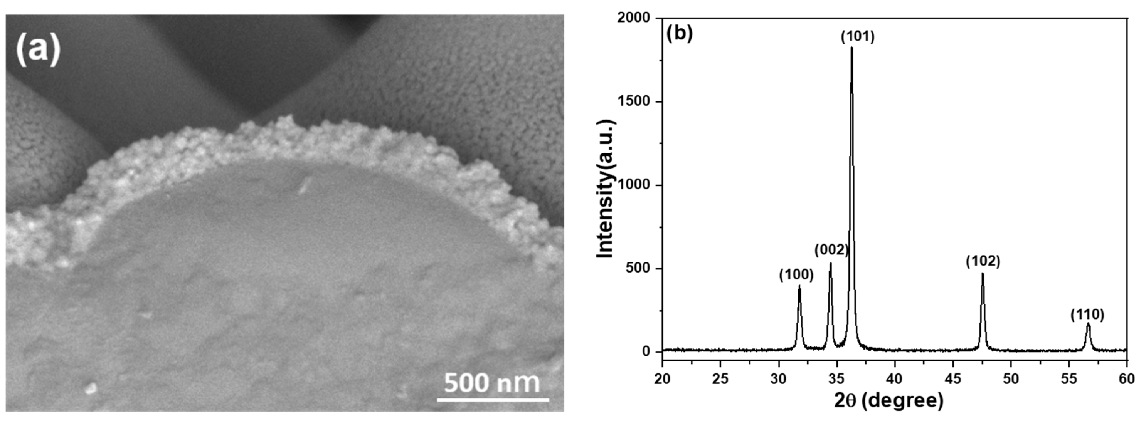
A ZnO seed layer was prepared by performing spin coating on the protrusion sapphire substrate, with a total of six coating cycles. Subsequently, the spin-coated ZnO gel underwent annealing at 300 °C, resulting in the formation of nano-crystalline particles, as illustrated in
Figure 3a. The resulting film had an average thickness of approximately 170 nm, with a deposition rate of around 28.3 nm per coating cycle. This information indicates the growth rate of ZnO seed layer during the spin-coating process. The X-ray diffraction (XRD) pattern of ZnO seed layer is presented in
Figure 3b. The pattern reveals a prominent diffraction peak corresponding to the (101) plane, rather than the (002) plane. Additional diffraction peaks are observed on the (100), (102), and (110) planes. These findings indicate that ZnO seed layer does not exhibit a preferred orientation of the c-axis. The size of crystalline particles in the nanoscale can be determined using the Debye–Scherrer equation, which is represented by D = (k λ/β cosθ). In this equation, D represents the size of the crystalline particles, β is Scherer’s constant (0.94), λ is the X-ray diffraction wavelength (1.54178 Å), and θ is the angle corresponding to the (002) diffraction peak observed in
Figure 3b. By inputting the FWHM (full width at half maximum) and θ values of the (002) diffraction peak into the Debye–Scherrer equation, the grain size of ZnO seed layer can be directly calculated. Based on the calculations, the grain size of ZnO seed layer is estimated to be approximately 54.9 nm.
Figure 4 depicts the top view of synthesized ZnO NRs as observed through scanning electron microscopy (SEM). From the visual representation provided in
Figure 4a,b, it is evident that ZnO NRs do not exhibit upward growth. Instead, they grow outwardly. This observation indicates that the growth directions of ZnO NRs are perpendicular to the ZnO seed layer, which is formed by the ZnO gel coated on the protruding sapphire substrate.
Figure 4a,b present a significant finding: the outward growth rates of ZnO NRs in different directions are nearly identical. Consequently, when viewed from the top, ZnO NRs exhibit a hexagonal appearance, highlighting the uniformity of their growth. While the hexagonal prism structure of ZnO NRs is evident, the precise reason for the distinctive appearance of an equilateral hexagon is not fully understood. However, one possible explanation is that as ZnO NRs grow, they undergo competition in all directions, leading to the initial formation of a hexagonal shape with a balanced distribution of energy. Furthermore, the grown ZnO NRs exhibit a hemisphere-like shape with outwardly protruding needle-like structures, ultimately giving rise to the formation of ZnO nanoflowers.
The specific mechanism behind this transformation and the factors influencing the shape and growth pattern of ZnO NRs and nanoflowers require further investigation. The sapphire substrate employed in the experiment possesses a distinctive structure characterized by protrusions arranged in a matrix pattern. This unique substrate structure influences the formation of ZnO nanoflowers, resulting in a matrix-like pattern resembling an array of ZnO nanoflowers. Upon examining the growth results presented in
Figure 4, it is observed that with increasing growth time, the width of the hexagonal edge lines decreases. When the growth time reaches one hour, ZnO nanoflowers grown from different protrusions begin to overlap, leading to the merging of adjacent hexagonal shapes. Consequently, the edge lines between the hexagonal shapes become indistinguishable or invisible due to the overlapping growth. As a result, the original structure of ZnO nanoflower matrix (NFM) becomes indiscernible, as illustrated in
Figure 4c. To quantify the surface characteristics of ZnO NFM, the specific surface areas were determined using the BET method. The measurements revealed specific surface areas of 11.6, 14.9, and 17.8 m
2/g for synthesis times of 30, 45, and 60 min, respectively. Based on these findings, we propose a hypothesis that the increase in the specific surface area of ZnO NFM is attributed to the longer ZnO nanorod length achieved through extended synthesis times. The longer nanorods contribute to a higher surface-to-volume ratio, resulting in an increased specific surface area.
Figure 5 displays the cross-sectional view of synthesized ZnO nanoflower-like structures (NFMs) using scanning electron microscopy (SEM). The measurements were conducted for synthesis times of 30, 45, and 60 min, and the obtained results are presented in
Figure 5a–c, respectively. For the synthesis time of 30, 45, and 60 min, the average lengths of ZnO NFMs were determined to be 343, 430, and 519 nm, respectively. The measured longest and shortest lengths were found to be 328 and 367 nm, 418 and 451 nm, and 505 and 542 nm, respectively. Additionally, the corresponding average diameters of ZnO NFMs were measured to be 108, 125, and 141 nm, and the largest and smallest diameters recorded were 104 and 113 nm, 120 and 128 nm, and 137 and 146 nm, respectively.
Table 2 gives the relevant results and the relationship between density and aspect ratio of ZnO NFMs with growth times of 30, 45, and 60 min. The phenomenon of two adjacent ZnO NRs combining into a single nanorod during the growth process contributes to this relationship. With longer growth times, there is a higher probability of nanorod combination, resulting in increased nanorod diameters but reduced overall density of ZnO NFMs.
This behavior is consistent with the findings presented in
Figure 4 and
Figure 5, which show the progressive merging and enlargement of ZnO NRs with longer growth times. Utilizing the parameters mentioned above, the total surface area and volume of ZnO NRs grown on the protrusion sapphire substrate can be estimated, as presented in
Table 2. For growth times of 30, 45, and 60 min, ZnO NRs densities were 127, 95, and 52 per μm
2, respectively. The estimated surface areas of ZnO NRs within an area of 1 μm
2 were 30.3, 40.59, and 51.65 μm
2, for the respective growth times. ZnO NRs grown on the protrusion sapphire substrate exhibit a nanoflower structure, resulting in a significantly larger total surface area than ZnO NRs grown in an upward direction, as illustrated in
Figure 4. Consequently, these ZnO NRs possess a larger contact area and can react with gases more effectively, thereby enhancing the sensing characteristics of gas sensors. The top areas of ZnO NRs grown on 1 μm
2 protrusion sapphire substrates were measured to be 0.76, 1.01, and 1.29 μm
2, respectively, while their corresponding volumes grown on the same substrates were 3.27, 5.07, and 7.28 μm
3, respectively.
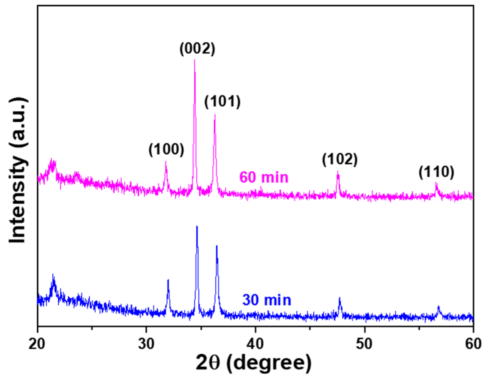
The X-ray diffraction (XRD) patterns of ZnO NRs synthesized on the sapphire protrusion substrate under different synthesis times were measured, and the results are displayed in
Figure 6. Comparing these results with
Figure 3b, it can be observed that the main diffraction peak shifted from the (101) plane to the (002) plane. Additionally, diffraction peaks corresponding to the (100), (102), and (110) planes were also observed. Furthermore,
Figure 6 illustrates that the diffraction intensity of the (002) plane increased significantly with synthesis time, indicating a preferred orientation along the c-axis of ZnO NRs. The diffraction intensities of the other four planes, namely (100), (101), (102), and (110), also exhibited slight increases with longer synthesis times. These findings suggest that the crystal structure of ZnO NRs is influenced by the growth duration, leading to changes in the dominant diffraction planes and their corresponding intensities. The crystalline properties of ZnO NRs can be determined using the biaxial strain model [
18]. In this model, stress is a crucial factor for the stability of ZnO NRs. In the case of ZnO NRs grown on the sapphire protrusion substrate, which exhibit a flower-shaped morphology as depicted in
Figure 4 and
Figure 5, the stress values are positive, indicating tensile forces acting on the nanorods. From
Figure 6, it can be observed that the 2θ value, FWHM value, grain size, and strain of ZnO nanoflower-like structures (NFMs) synthesized for 60 min were measured as 36.21°, 0.035°, 36.9 nm, and 1.502 GPa, respectively. These parameters provide insights into the crystal properties and mechanical stability of 60 min-synthesized ZnO NFMs.
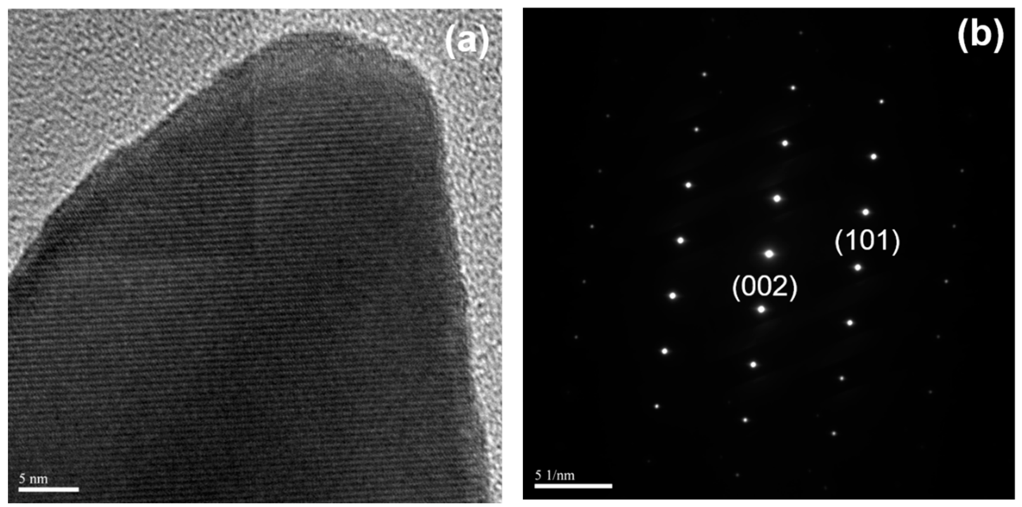
High-resolution electron microscopy was utilized to conduct measurements on the lattice fringe widths. The high-resolution TEM micrographs were captured using a field emission gun operated at an acceleration voltage of 200 kV. The obtained results are presented in
Figure 7a, while
Figure 7b illustrates the processed fast Fourier transformation of the corresponding image. The observed lattice spacing measures 2.58 Å, indicating the presence of (002) planes within the Wurtzite structure.
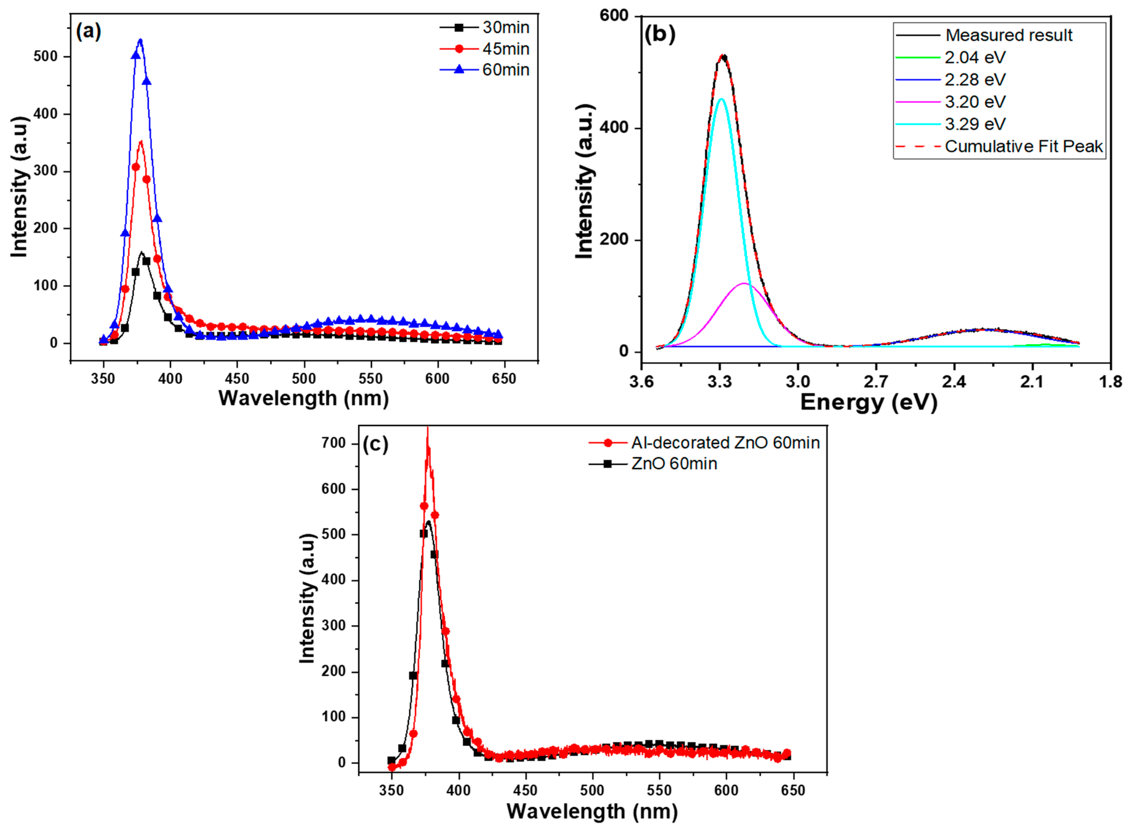
The photoluminescence (PL) spectra of ZnO NFMs synthesized at different times are shown in
Figure 8a, where a UV light of 325 nm was used as the excitation source. The spectra exhibit two distinct emission peaks. The first peak, denoted as I
UV, is located at a wavelength of approximately 380 nm and exhibits a strong intensity. This peak arises from the recombination of free excitons [
19], indicating a near-band-edge emission characteristic of ultraviolet (UV) light. It is a typical emission observed in ZnO materials. The second peak, spanning from approximately 450 nm to 600 nm, corresponds to a green light emission (I
G). This emission is attributed to the presence of various defects within synthesized ZnO NFMs. The defects in the material contribute to the energy levels and transitions that result in the emission of green light. Overall, the PL spectra provide valuable information about the optical properties and defect states of ZnO NFMs synthesized at different time durations. As shown in
Figure 8a, the I
G value, corresponding to the green light emission, increases with the growth time of ZnO NFMs. This indicates that the number of defects in ZnO NFMs increases as the growth time extends. To understand the underlying reasons for this observation, further investigations are needed. Previous studies have indicated that different mechanisms can lead to various emissions in ZnO-based materials [
20,
21].
In this context,
Figure 6 demonstrates that both the I
UV and I
G values increase with the growth time. The I
UV peaks are observed at wavelengths of 378.2, 378.0, and 377.8 nm for growth times of 30, 45, and 60 min, respectively. To understand the specific mechanisms responsible for the emissions, further analysis and characterization are required. These could include studying the defect types and concentrations, investigating the influence of growth conditions, and examining the impact of structural changes on the optical properties of ZnO NFMs. Additionally, the full width at half maximum values for the I
UV peaks in the PL spectra were measured. For growth times of 30, 45, and 60 min, the FWHM values were 19.1 nm (371.5–390.6 nm), 29.5 nm (369.3–397.8 nm), and 37.5 nm (367.4–384.9 nm), respectively. These results indicate that as the growth time increases, the FWHM value also increases. It is worth noting that this result differs significantly from the previous observation of the IG values, which showed a decrease with longer growth times. One possible explanation for this discrepancy is the difference in the substrate structure used in this study compared to previous research [
22]. The substrate structure can have a significant impact on the growth process and the resulting optical properties of ZnO NFMs, leading to varying trends in the PL spectra.
In
Figure 8b, the PL spectrum of ZnO NFMs synthesized at 60 min is plotted with energy (eV) as the x-axis. To analyze this spectrum, a fitting procedure was performed on the merged emission profile in the range of approximately 3.54–1.91 eV (350–650 nm). The fitting was carried out using four Gaussian functions positioned at approximately 3.29, 3.20, 2.28, and 2.04 eV, respectively. It is important to note that the intensity of the band at 2.04 eV, attributed to the recombination of
ions with delocalized electrons [
23], was found to be small in the fitting result, and its effect could be neglected. Purbayanto et al. discovered that the emission peak at 3.251 eV is associated with two-electron satellite transitions and donor-acceptor pair transitions [
24]. The peaks at 3.29 eV, 3.20 eV, and 2.28 eV are believed to be caused by near-band-edge emission, zinc vacancies (V
Zn), and interstitial oxygen (O
i), respectively [
20,
21]. However, in 60 min-synthesized ZnO NFMs, the peaks corresponding to oxygen vacancy (V
O) with an energy gap (Eg) of approximately 1.62 eV, antisite defects (O
Zn) with Eg of ~2.38 eV, interstitial zinc (Zn
i) with Eg of ~2.90 eV, and zinc vacancy (V
Zn) with Eg of ~3.06 eV were not observed.
In
Figure 8a, it is evident that the intensity of the green emission peak increases with the growth time of ZnO NFMs. This suggests that as the synthesis time increases, the amount of interstitial oxygen in the grown ZnO NFMs decreases. The intensities of I
G and I
UV and the I
G/I
UV ratio of ZnO NFMs were measured as a function of synthesis time. With the increase in growth time from 30 min to 60 min, the intensity of the IUV value increased from 160 to 529 (a.u.), while the IG value increased from 16.2 to 41.6. Consequently, the I
G/I
UV ratio decreased from 0.101 to 0.079.
Figure 8c presents a comparison between 60 min-synthesized ZnO NFMs without and with Al decoration. The I
UV value significantly increased to 710 when Al was used to decorate ZnO NFM, while the I
G value showed no apparent change. This result from
Figure 7c suggests that Al decoration has a noticeable effect on the I
UV value of a ZnO NFM. Consequently, the Al decoration is likely to impact the sensing properties of synthesized ZnO NFMs.
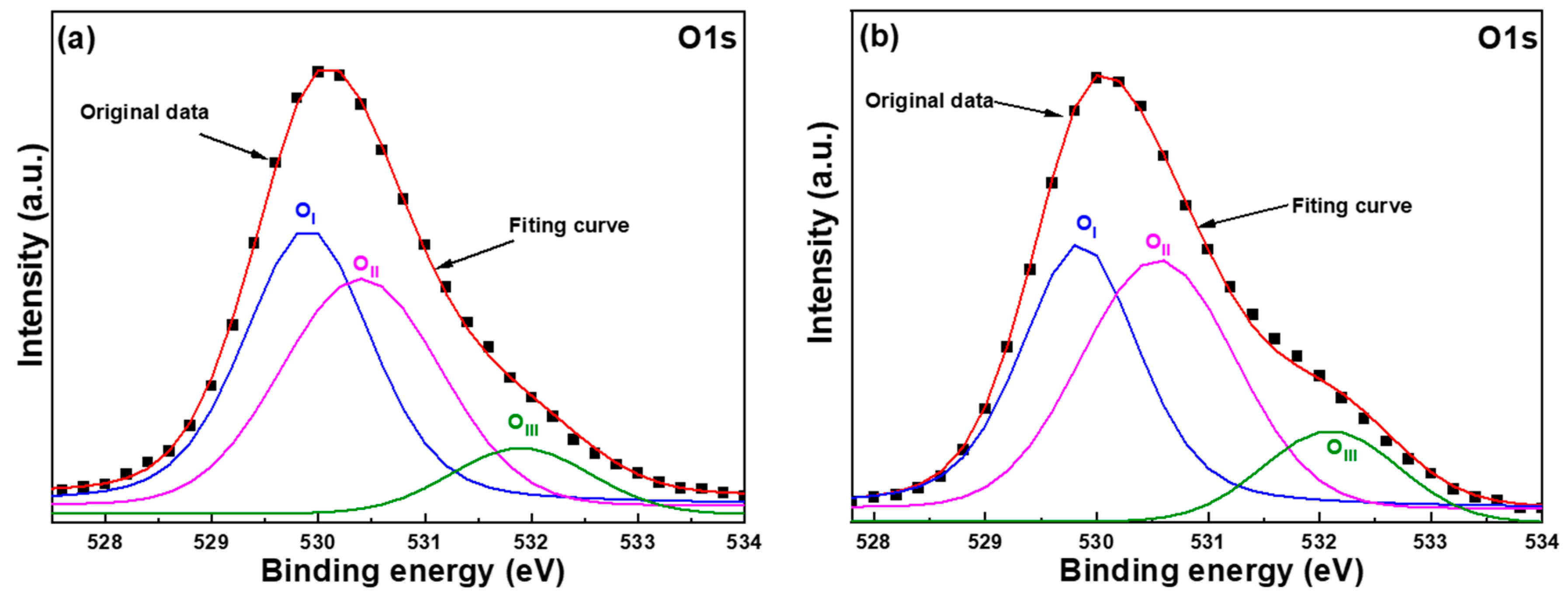
We conducted X-ray photoelectron spectroscopy (XPS) to analyze the chemical bonding state of oxygen in order to investigate the effect of synthesis time. This analysis helps establish a relationship between defects caused by different synthesis times and the optical properties of ZnO NFMs. The O1s peak of ZnO NFMs was measured for samples synthesized for 30 min and 60 min, and the corresponding results are illustrated in the accompanying diagrams. The typical surface O
1s peaks of ZnO NFMs are centered at 530.1 ± 0.1 eV and fitted by three Gaussian components of O
I, O
II, and O
III peaks, as
Figure 9a,b shows, which are centered at 529.7 ± 0.1 eV, 530.2 ± 0.2 eV, and 532.2 ± 0.2 eV, respectively. For ZnO NFMs, the bond energy for components of O
I, O
II, and O
III peaks are caused by the Zn
2+-O
2− bond, the oxygen vacancies, and the chemical absorption of oxygen on the surfaces [
25].
Table 3 presents a comparison of the areas of O
1s peaks measured from the XPS spectra of ZnO NFMs as a function of synthesis time. With an increase in synthesis time from 30 min to 60 min, the area of the OI peak decreases from 48.89% to 45.62%, the area of the OII peak increases from 41.48% to 43.08%, and the area of the OIII peak increases from 9.63% to 11.30%. The observed increase in the area of the OII peak of ZnO NFMs with the increase in synthesis time provides evidence that the oxygen vacancies in ZnO NFMs increase over time. This suggests that the defects in ZnO NFMs also increase with longer synthesis times. Furthermore, since the oxygen vacancies increase with synthesis time, these results indirectly support the finding that the intensity of the I
G value in ZnO NFMs increases with synthesis time, which is consistent with the measured results shown in
Figure 8.
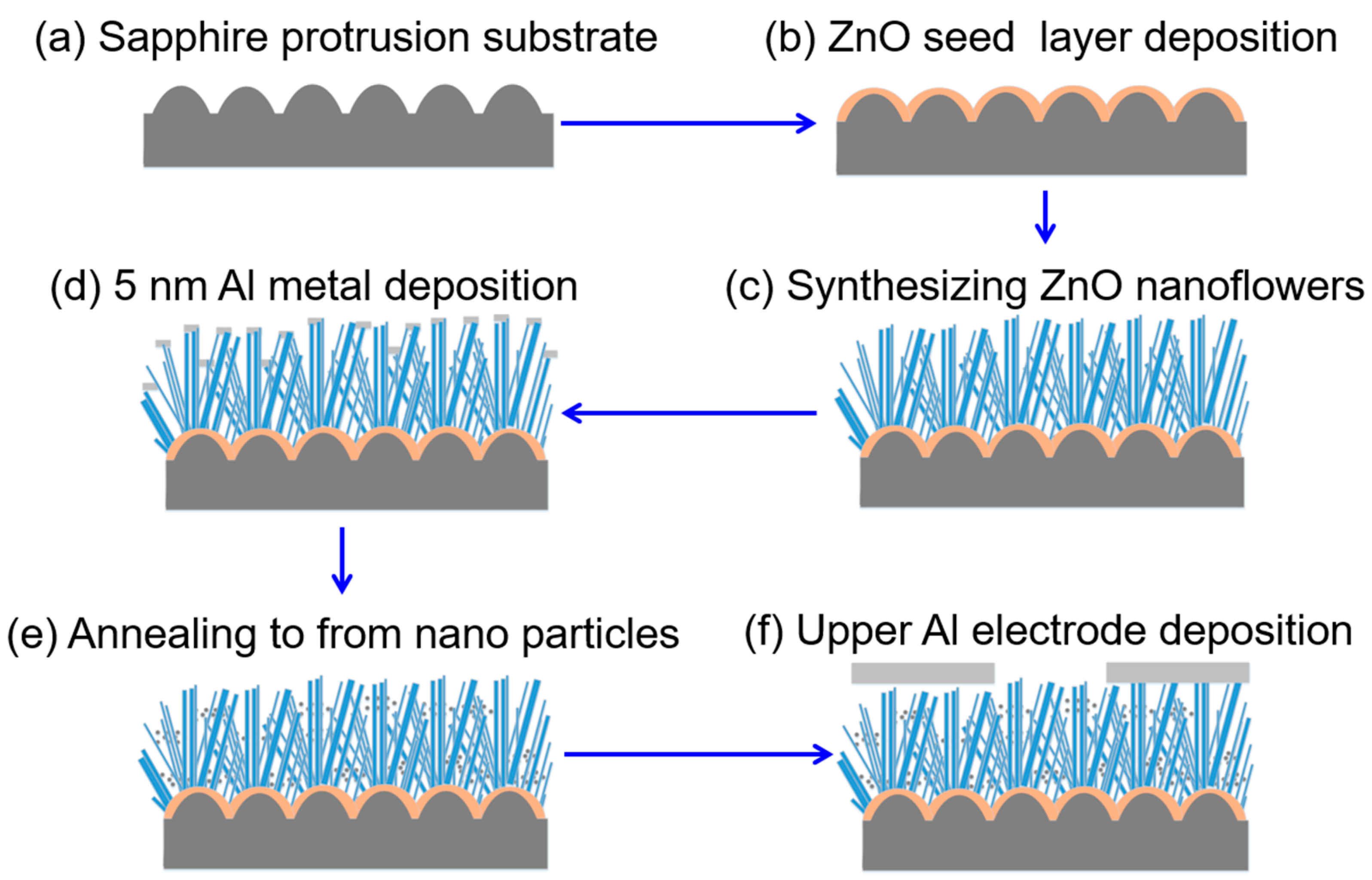
In this study, the thermal evaporation method was employed to deposit a 5 nm thick Al film on ZnO NFMs. Subsequently, the Al film was coated and annealed, and the diameter of the formed Al nanoparticles (NPs) was calculated using XRD diffraction patterns.
Figure 10a–c present the surface morphologies of Al-decorated ZnO NFMs synthesized for 30, 45, and 60 min, respectively. The diameters of the nano-Al particles on Al-decorated ZnO NFMs were measured as 29.91, 34.8, and 42.7 nm for the respective growth times of 30, 45, and 60 min, respectively.
When 30 min- and 45-min synthesized ZnO NFMs were used as the sensing devices to detect the CO (H
2) gas, they took approximately 237 and 196 s (225 and 188 s, resistance falling time) for the resistance to drop from 252 (248) and 143 (141) kΩ to around 187 (184) and 96.7 (95.3) kΩ at the first cycle. We find that the response time is long, and the response rates for CO (H
2) are 1.348 (1.347) and 1.479 (1.480), respectively. As compared with the sensing results of 60-min synthesized ZnO NFMs, we have identified two significant issues: the response rates of both groups are relatively lower and the resistance values of both groups are relatively high, leading to considerable response rate and resistance drifts during testing processes. Consequently, we have excluded these two sets of sensors from further use and comparison.
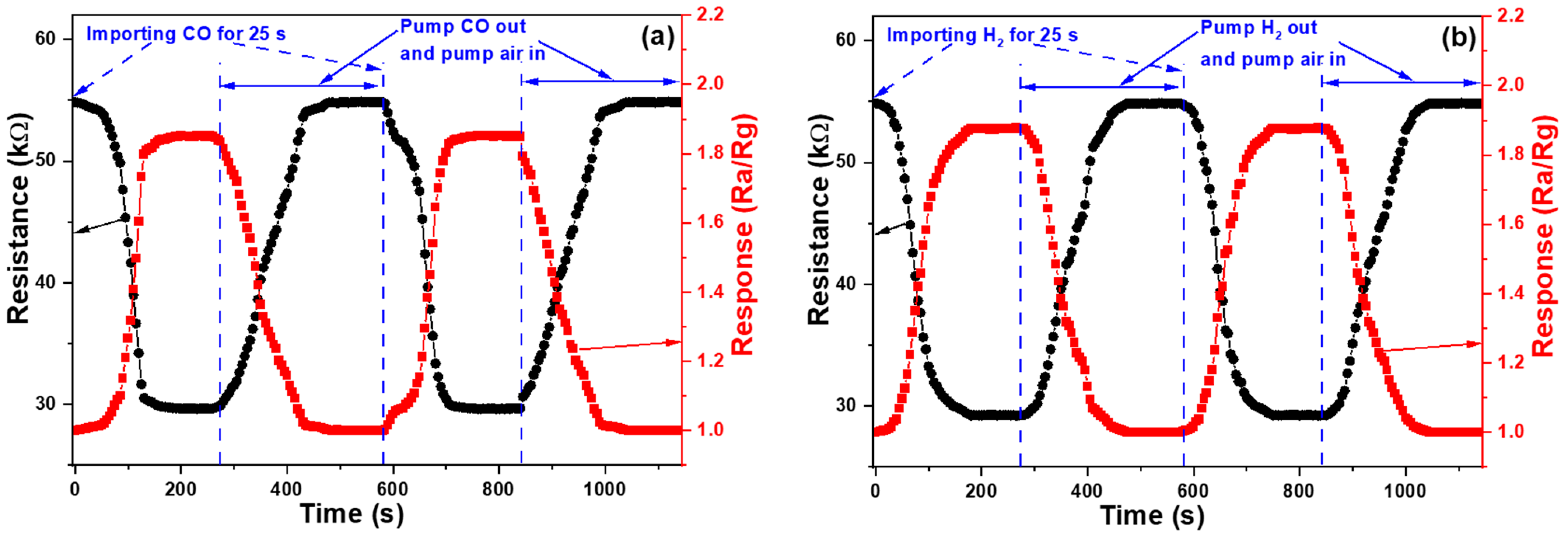
Figure 11 illustrates the CO and H
2 gas sensing properties of undecorated ZnO NFM grown on a sapphire convex substrate for 60 min. In
Figure 11a, when 2000 ppm of CO was introduced, it reacted with the oxygen ions adsorbed on ZnO NFM, releasing electrons to the zinc oxide and causing the resistance to decrease. It took approximately 130 s for the resistance to drop from 54.83 kΩ to around 30.52 kΩ at the first cycle. Subsequently, after pumping out the CO and introducing air, the resistance value gradually returned to about 51.65 kΩ after approximately 115 s (resistance rising time). These test results were also used to evaluate the reproducibility of the component, which involved testing the component repeatedly for 10 cycles to determine whether the resistance value and response rate remained stable. The average resistance values for the 10 (100) cycles were found to be 54.9 (55.3) and 31.2 (33.4) kΩ for the high and low values and the average resistance falling and rising times were 132 (134) and 118 (121) s, respectively. These results demonstrate that the gas sensors fabricated using ZnO NFM can be used repeatedly. The comparisons of response properties of ZnO NFM-based sensors under different synthesis times at the first measurement round are compared in
Table 4.
In
Figure 11b, the oxygen ions began to combine with the H
2 molecules, which were introduced at a concentration of 2000 ppm, adsorbed on ZnO NFM and released electrons to ZnO NFM, and as a result, the resistance started to decrease. As shown
Figure 11a, the resistance decreased from 54.86 kΩ to approximately 30.70 kΩ in about 130 s at first cycle. Subsequently, the H
2 was removed, and air was introduced, which caused the resistance value to recover to approximately 51.58 kΩ after 125 s. These test results were also subjected to device reproducibility testing, which involved repeating the test for the gas sensors ten times to determine whether the device’s resistance values and response change rates were stable. It was found that the average high and low resistance values for the 10 (100) cycles were 55.6 (53.7) and 56.1 (33.1) kΩ and the average resistance falling and rising times were 133 (136) and 128 (131) s, respectively, which demonstrated that the device was also reusable for H
2 sensing. The response rates of CO and H
2 sensing for 60 min-growth undecorated ZnO NFM are also shown in
Figure 11. The maximum response rates of CO and H
2 for sensing at first cycle were 1.796 and 1.788, the average maximum response rates for the 10 cycles of CO and H
2 sensing were 1.759 (which is 95.1% of 1.796) and 1.782 (which is 94.9% of 1.788), and the average maximum response rates for the 100 cycles of CO and H
2 sensing were 1.656 (89.5%) and 1.695 (90.3%), respectively.
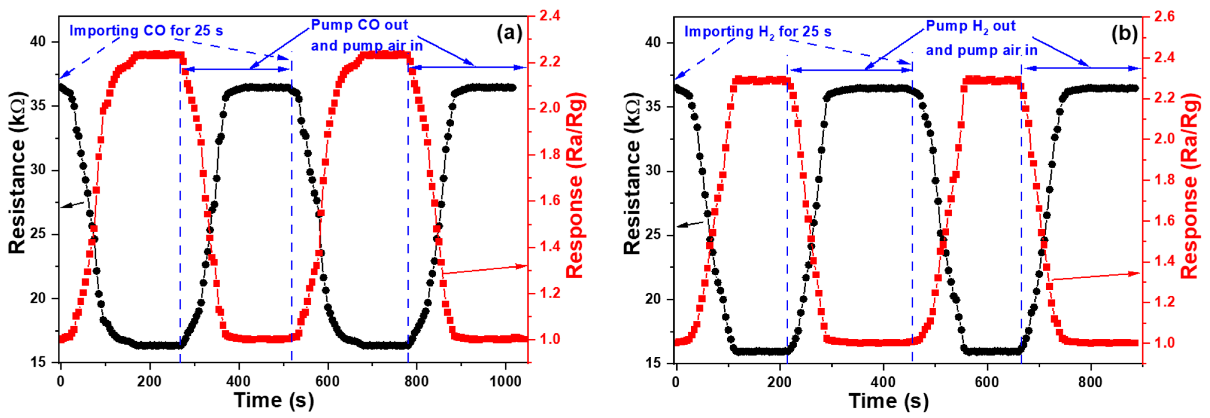
Figure 12 shows the sensing characteristics of ZnO NFM gas sensors decorated with Al NPs and grown for 60 min. As
Figure 12a shows, after 2000 ppm of CO was introduced, the resistance began to decrease, and it took about 120 s to drop from 34.5 to about 17.2 kΩ. Then the CO was pumped out and air was introduced, and the resistance value returned to about 34.34 kΩ after about 90 s. The average high and low resistance values for the 10 (100) cycles CO sensing were 34.8 (35.2) and 17.9 (18.9) kΩ and the average resistance falling and rising times were 122 (124) and 91 (93) s, respectively, which demonstrated that the device was also reusable for CO sensing. It can also be seen from
Figure 12b that after the introduction of 2000 ppm of H
2, the resistance started to decrease, and it took about 105 s to drop from 36.5 kΩ to about 16.9 kΩ. Then H
2 was pumped out and air was introduced, and the resistance value returned to about 36.0 kΩ after about 65 s. The average high and low resistance values for the 10 (100) cycles H
2 sensing were 37.1 (38.0) and 17.8 (18.9) kΩ and the average resistance falling and rising times were 106 (108) and 64 (66) s. Comparing the sensing results in
Figure 11 and
Figure 12, we find that Al-decorated ZnO NFM gas sensors have lower resistance, faster response times, and higher response rates in the sensing processes of CO and H
2 gases. The maximum response rates of CO and H
2 for sensing at first cycle were 2.006 and 2.160, the average maximum response rates for the 10 cycles of CO and H
2 sensing were 1.942 (which is 96.8% of 2.006) and 2.087 (which is 96.6% of 2.160), and the average maximum response rates for the 100 cycles of CO and H
2 sensing were 1.862 (92.8%) and 2.009 (93.0%), respectively. These results in
Figure 11 and
Figure 12 prove that the Al-decorated ZnO NFMs have a higher response rate, a shorter response time, and higher cycling stability.
The inductive properties of metal oxide semiconductors are mainly due to the phenomenon of charge transfer caused by the adsorption and desorption of oxygen atoms on metal oxides, which in turn changes the electrical properties [
3,
25]. Oxygen atoms adsorb on the surface of the oxide structure and trap electrons, forming oxygen ions that can reduce the electrical conductivity of metal oxide semiconductors. When the metal oxide semiconductors are exposed to the environment of reducing gases such as CO, the CO gas molecules will react with the adsorbed oxygen ions to form carbon dioxide CO
2, which will lead to the release of electrons and improve the conductivity. Takata et al. found that oxygen ions exist in the form of O
2− in low temperature environments (below 100 °C) [
26]. When the temperature is between 100–300 °C, it will exist in the form of O
− ions, and when the temperature is higher than 300 °C, it will transform into O
2− ions [
27]. The reaction of CO to oxygen ions at various temperatures is shown in the following reactions.
Because the test temperature is 200 °C, the main reason for the drop in resistance of ZnO NFM gas sensors is the reaction Formula (4). The induction mechanism of H2 is the same, mainly that the electrons reduced on the surfaces of ZnO NRs will be released to the conduction band and help to increase the current flowing through ZnO NRs.
A larger specific surface area provides more sites for gaseous molecules to be adsorbed, while a smaller crystal size (approximately equal to the Debye length λ
D) results in total depletion, leading to higher sensitivity. The Debye length λ
D, which is calculated using the equation λ
D = {2k
BT/e
2N
d}
1/2, is strongly influenced by the carrier density (N
d). Here, k
B is the Boltzmann constant, T is the absolute temperature, and e is the electron charge [
5]. Therefore, by controlling the carrier density, the effective Debye length of the oxide can be adjusted to maximize the gas sensing response. For instance, increasing the carrier density can decrease the Debye length, which is equivalent to increasing the effective crystal size of the material. As noted earlier, the Debye length depends on the concentration of carriers, which means that the introduction of various metal decorations on the surfaces of the fabricated samples will change the concentration of carriers. However, regardless of the type of metal used, decorating the surface of ZnO NRs with metal will elevate the carrier concentration (electrons in the metal), and that will lead to a shorter Debye length and improve efficiency in gas sensing.
