
A 5.8 GHz 1.8 V +20 dBm 32.5% PAE Power Amplifier for a Short-Range Over-the-Air WPT Application

 , ,
, , 
Abstract
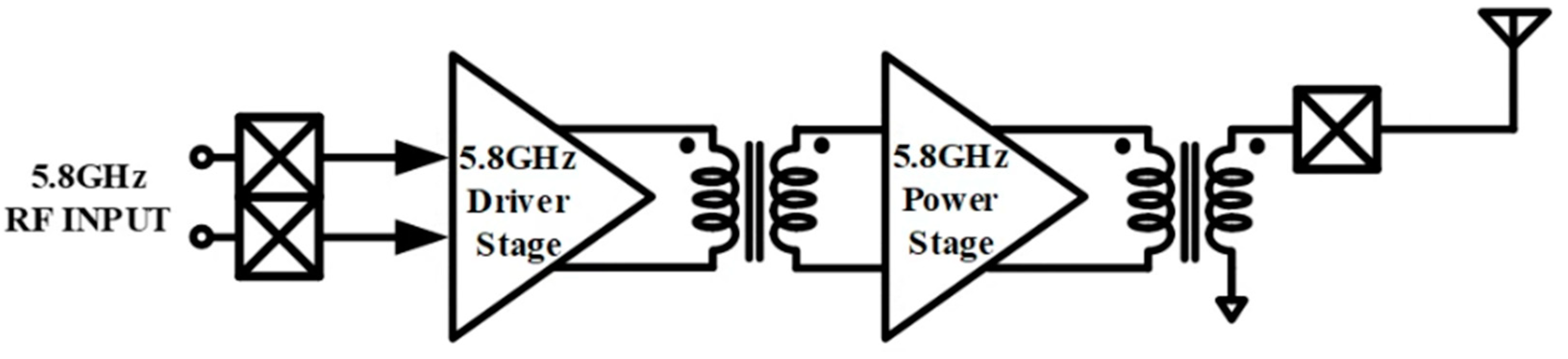
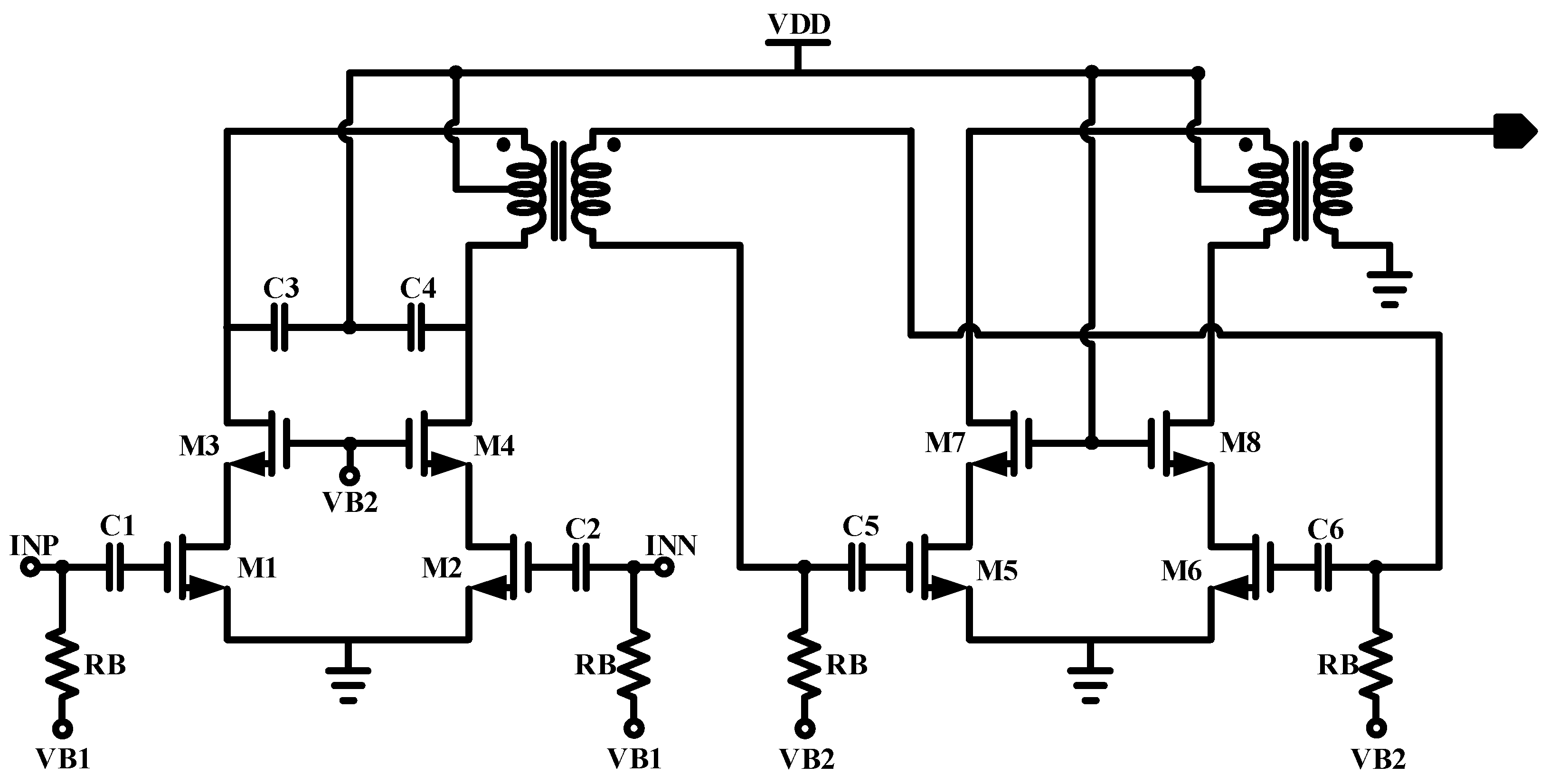
:1. Introduction
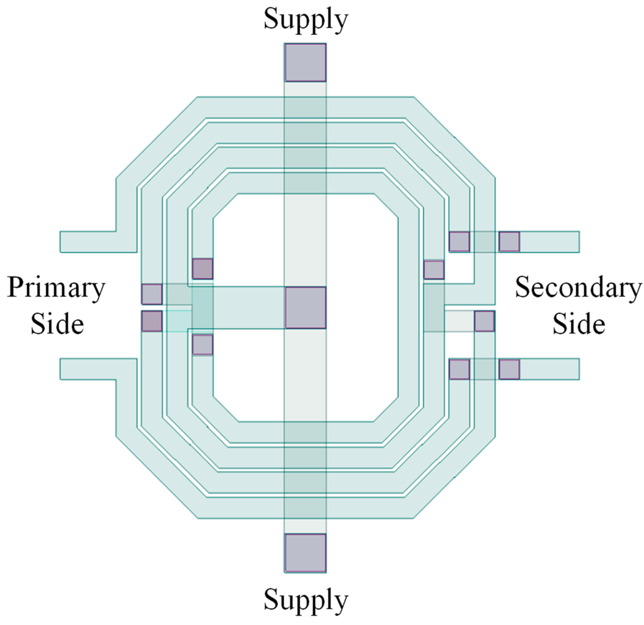
2. Proposed Power-Amplifier Structure
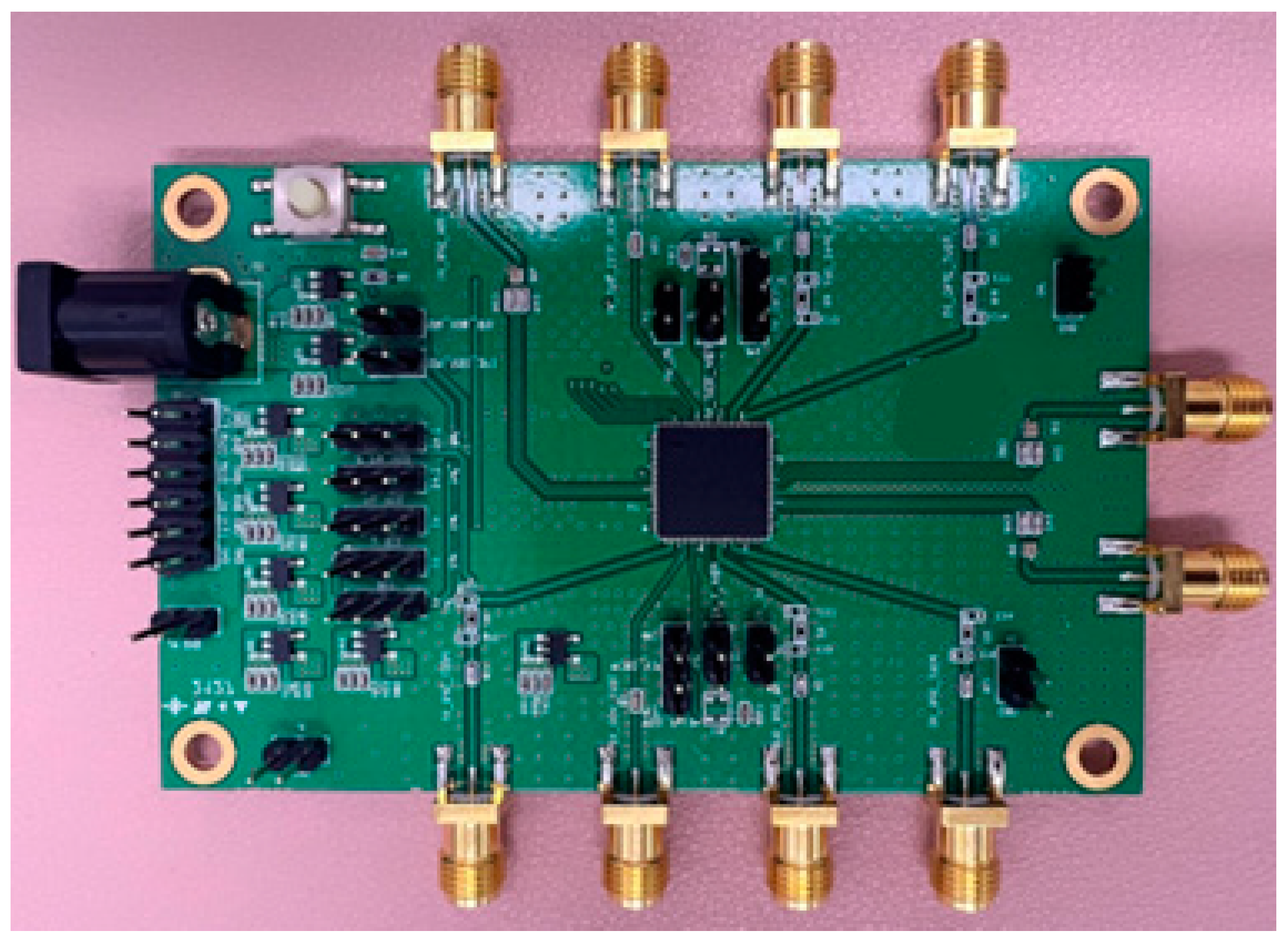
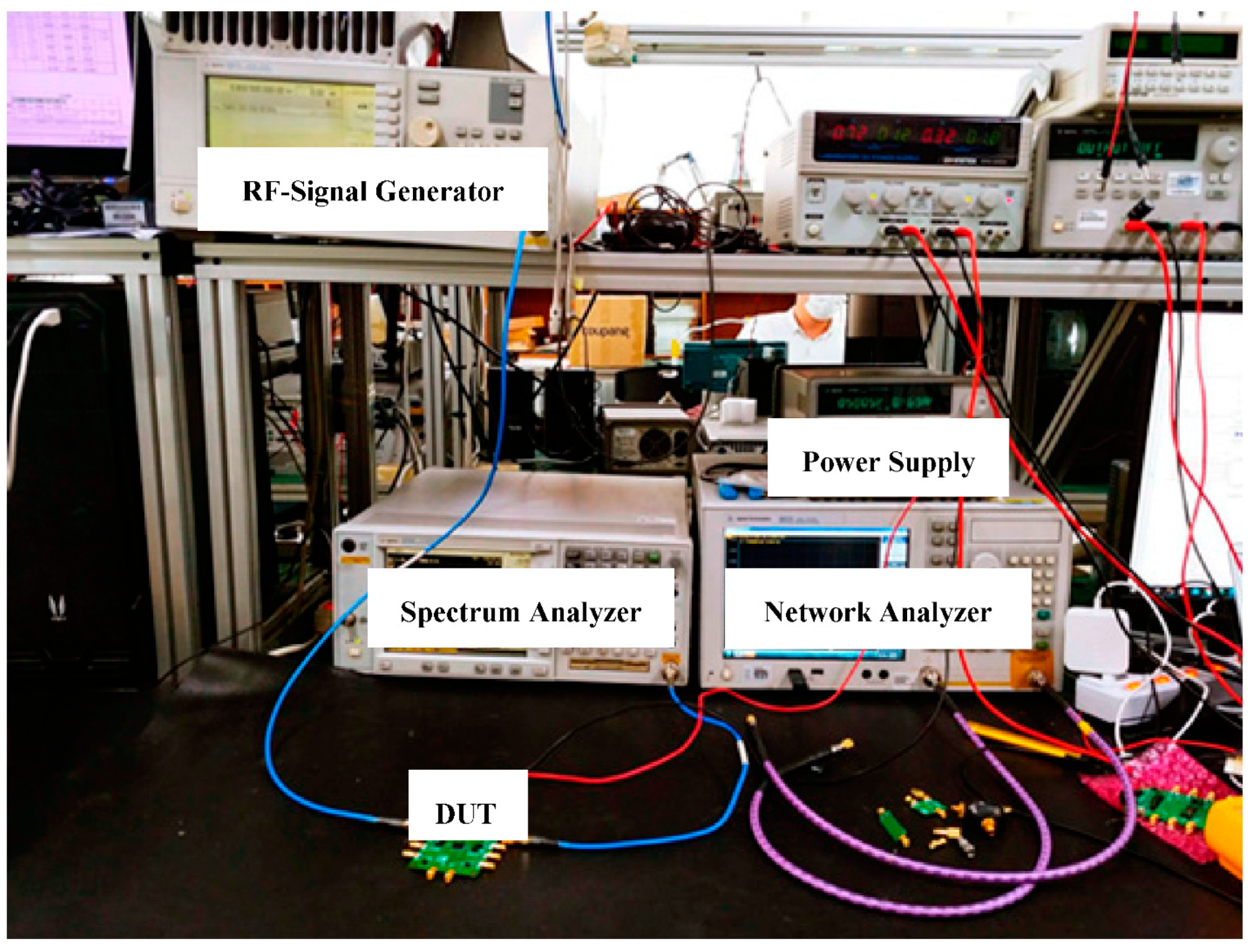
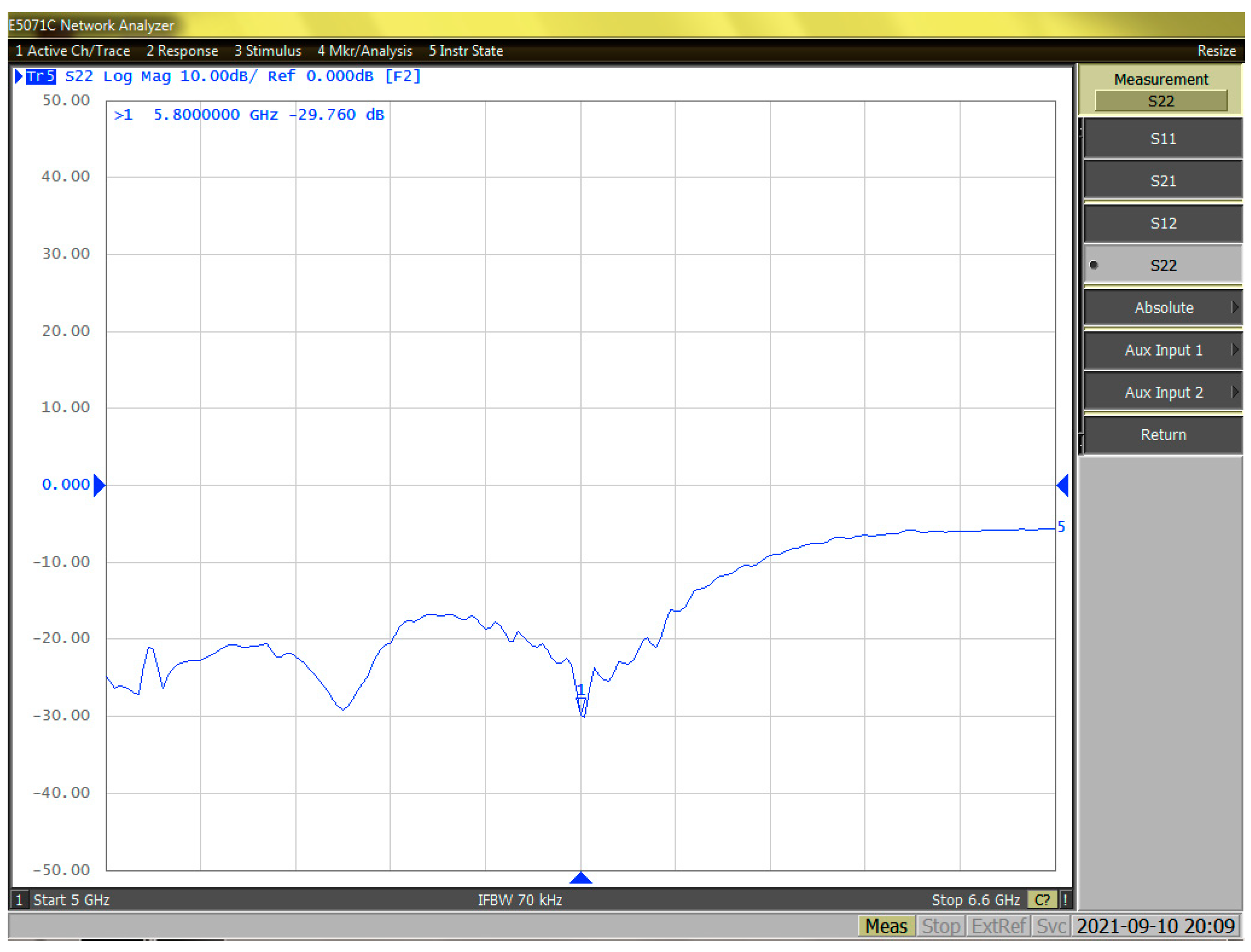
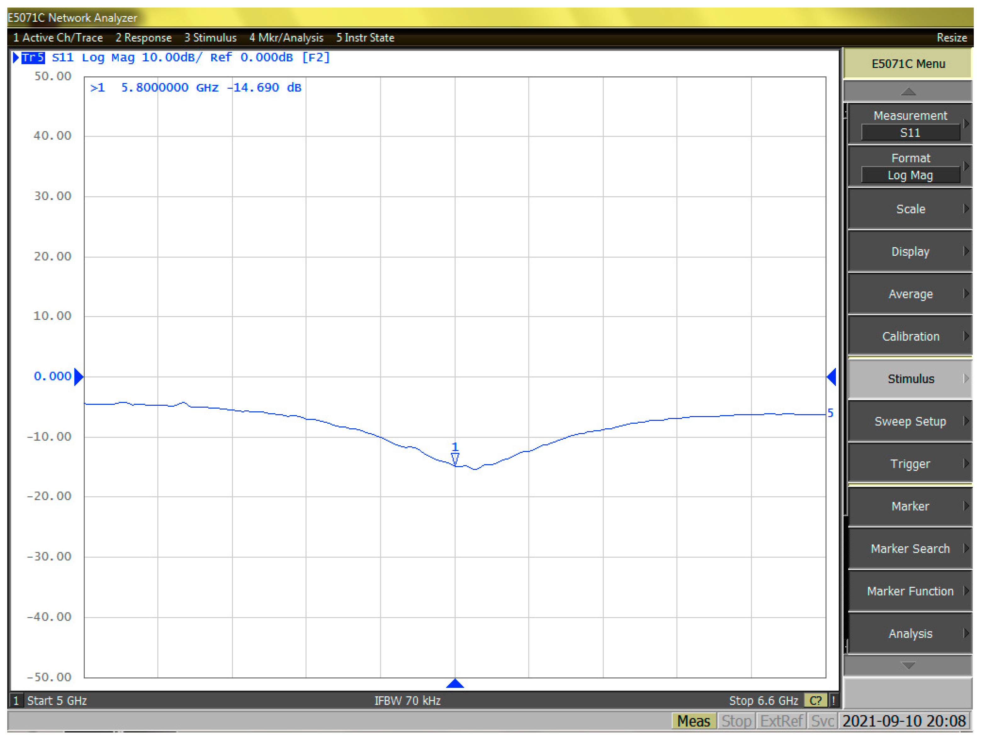
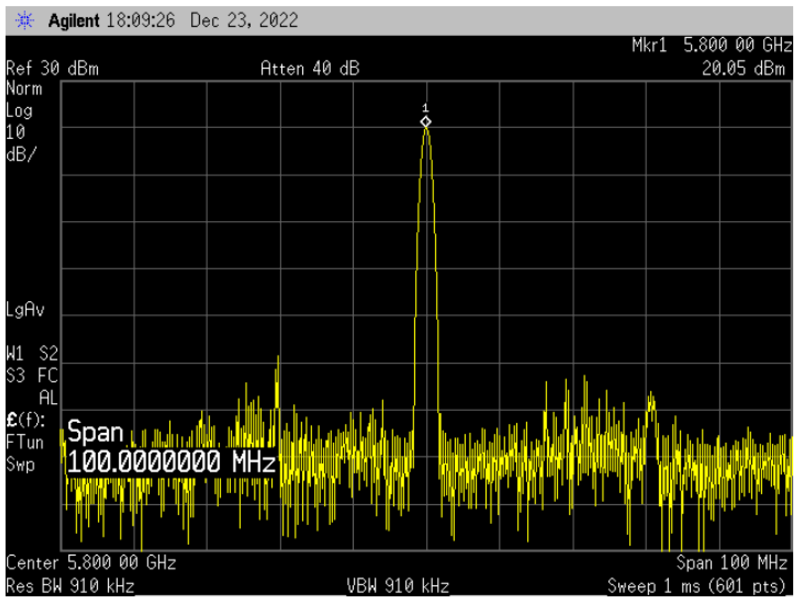
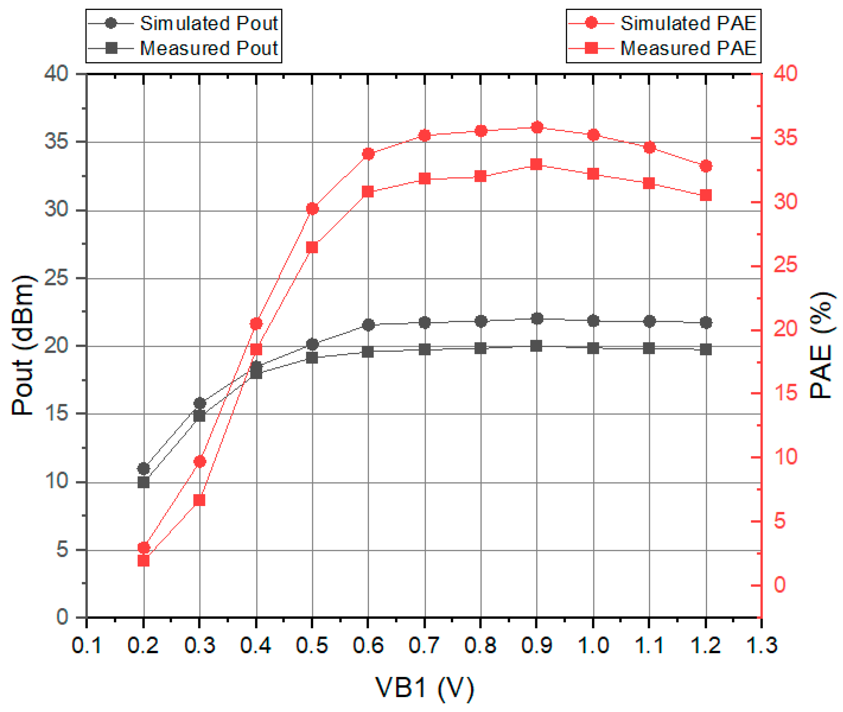
3. Measurement Results
4. Conclusions
Author Contributions
Funding
Institutional Review Board Statement
Informed Consent Statement
Data Availability Statement
Conflicts of Interest
References
- Jang, B.; Hejazi, A.; Rad, R.E.; Qaragoez, Y.M.; Ali, I.; Pu, Y.; Hwang, K.C.; Yang, Y.; Lee, K.-Y. A 15-W Triple-Mode Wireless Power Transmitting Unit with High System Efficiency Using Integrated Power Amplifier and DC–DC Converter. IEEE Trans. Ind. Electron. 2021, 68, 9574–9585. [Google Scholar] [CrossRef]
- Valenta, R.; Durgin, G.D. Harvesting Wireless Power: Survey of Energy-Harvester Conversion Efficiency in Far-Field, Wireless Power Transfer Systems. IEEE Microw. Mag. 2014, 15, 108–120. [Google Scholar] [CrossRef]
- Rad, R.E.; Kim, S.; Rikan, B.S.; Lee, K.-Y. A High Power High Efficient 5.8 GHz CMOS Class-A Power Amplifier for a WPT Application. In Proceedings of the 2021 Twelfth International Conference on Ubiquitous and Future Networks (ICUFN), Porto, Portugal, 29 June–2 July 2021; pp. 184–186. [Google Scholar] [CrossRef]
- Hejazi, A.; Jang, B.; Rad, R.E.; Jo, J.; Rikan, B.S.; Pu, Y.; Yoo, S.-S.; Hwang, K.C.; Yang, Y.; Lee, K.-Y. A 2.4 GHz Power Receiver Embedded with a Low-Power Transmitter and PCE of 53.8%, for Wireless Charging of IoT/Wearable Devices. IEEE Trans. Microw. Theory Tech. 2021, 69, 4315–4325. [Google Scholar] [CrossRef]
- Kiani, M. Wireless Power Transfer and Management for Medical Applications: Wireless power. IEEE Solid-State Circuits Mag. 2022, 14, 41–52. [Google Scholar] [CrossRef]
- Meng, M.; Kiani, M. A Hybrid Inductive-Ultrasonic Link for Wireless Power Transmission to Millimeter-Sized Biomedical Implants. IEEE Trans. Circuits Syst. II Express Briefs 2017, 64, 1137–1141. [Google Scholar] [CrossRef]
- Ibrahim, A.; Kiani, M.; Farajidavar, A. A 64-channel wireless implantable system-on-chip for gastric electrical-wave recording. In Proceedings of the 2016 IEEE Sensors, Orlando, FL, USA, 30 October–3 November 2016; pp. 1–3. [Google Scholar] [CrossRef]
- Springston, C.S.; Bao, R.; Farajidavar, A. A 32-channel wireless system for recording gastric electrical activity. In Proceedings of the 2016 38th Annual International Conference of the IEEE Engineering in Medicine and Biology Society (EMBC), Orlando, FL, USA, 16–20 August 2016; pp. 1971–1974. [Google Scholar] [CrossRef]
- Jia, Y.; Mirbozorgi, A.; Lee, B.; Khan, W.; Madi, F.M.; Weber, A.; Li, W.; Ghovanloo, M. A mm-sized free-floating wirelessly powered implantable optical stimulating system-on-a-chip. In Proceedings of the 2018 IEEE International Solid—State Circuits Conference—(ISSCC), San Francisco, CA, USA, 11–15 February 2018; pp. 468–470. [Google Scholar] [CrossRef]
- Mirbozorgi, S.A.; Jia, Y.; Ghovanloo, M. Power Efficiency and Power Delivery Measurement in Inductive Links with Arbitrary Source and Load Impedance Values. In Proceedings of the 2018 IEEE Life Sciences Conference (LSC), Montreal, QC, Canada, 10–30 October 2018; pp. 25–28. [Google Scholar] [CrossRef]
- Hajimiri, A.; Abiri, B.; Bohn, F.; Gal-Katziri, M.; Manohara, M.H. Dynamic Focusing of Large Arrays for Wireless Power Transfer and Beyond. IEEE J. Solid-State Circuits 2021, 56, 2077–2101. [Google Scholar] [CrossRef]
- Bohn, F.; Abiri, B.; Hajimiri, A. Fully integrated CMOS X-Band power amplifier quad with current reuse and dynamic digital feedback (DDF) capabilities. In Proceedings of the 2017 IEEE Radio Frequency Integrated Circuits Symposium (RFIC), Honolulu, HI, USA, 4–6 June 2017; pp. 208–211. [Google Scholar] [CrossRef]
- Park, S.; Jeon, S. Wideband harmonic-tuned CMOS power amplifier with 19.5 dBm output power and 22.6% PAE over entire X-band. IET Electron. Lett. 2015, 51, 703–705. [Google Scholar] [CrossRef]
- Comeau, J.P.; Thoenes, E.W.; Imhoff, A.; Morton, M.A. X-Band +24dBm CMOS Power Amplifier with Transformer Power Combining. In Proceedings of the 2011 IEEE 11th Topical Meeting on Silicon Monolithic Integrated Circuits in RF Systems, Glendale, AZ, USA, 17–19 January 2011; pp. 49–52. [Google Scholar]
- Chen, J.-H.; Helmi, S.R.; Jou, A.Y.-S.; Mohammadi, S. A Wideband Power Amplifier in 45 nm CMOS SOI Technology for X Band Applications. IEEE Microwave Wirel. Comp. Lett. 2013, 23, 587–589. [Google Scholar] [CrossRef]
- Park, S.; Jeon, S. A full X-band CMOS amplifier with wideband class-E harmonic matching Microw. Opt. Technol. Lett. 2015, 57, 645–649. [Google Scholar] [CrossRef]
- Park, J.; Park, C. An X-band CMOS power amplifier with a driver stage using a shot-through current rejection technique. Microw. Opt. Technol. Lett. 2014, 56, 1159–1162. [Google Scholar] [CrossRef]


| Parameters | [13] | [14] | [15] | [16] | [17] | This Work |
|---|---|---|---|---|---|---|
| Technology | 110 nm CMOS | 180 nm CMOS | 45 nm SOI-CMOS | 110 nm CMOS | 130 nm CMOS | 180 nm CMOS |
| Supply Voltage (V) | 2.6 | 3 | 4.8 | 2.3 | 2 | 1.8 |
| Frequency (GHz) | 9 | 10 | 12 | 9 | 12 | 5.8 |
| Power Gian (dB) | 11.6 | 25 | 9.8 | 10.6 | 17 | 20.05 |
| Peak Output Power (dBm) | 20.3 | 24.5 | 22.8 | 12.4 | 14 | 20.05 |
| Peak PAE (%) | 28.9 | 18 | 21.8 | 20.2 | 27 | 32.5 |
| F.O.M. | 245.59 | 262 | 247.56 | 235.13 | 245.63 | 250.48 |
Disclaimer/Publisher’s Note: The statements, opinions and data contained in all publications are solely those of the individual author(s) and contributor(s) and not of MDPI and/or the editor(s). MDPI and/or the editor(s) disclaim responsibility for any injury to people or property resulting from any ideas, methods, instructions or products referred to in the content. |
© 2023 by the authors. Licensee MDPI, Basel, Switzerland. This article is an open access article distributed under the terms and conditions of the Creative Commons Attribution (CC BY) license (https://creativecommons.org/licenses/by/4.0/).
Share and Cite
Kim, M.; Rad, R.E.; Kim, S.; Pu, Y.; Jung, Y.; Huh, H.; Yoo, J.; Kim, S.; Lee, K. A 5.8 GHz 1.8 V +20 dBm 32.5% PAE Power Amplifier for a Short-Range Over-the-Air WPT Application. Sensors 2023, 23, 5279. https://doi.org/10.3390/s23115279
Kim M, Rad RE, Kim S, Pu Y, Jung Y, Huh H, Yoo J, Kim S, Lee K. A 5.8 GHz 1.8 V +20 dBm 32.5% PAE Power Amplifier for a Short-Range Over-the-Air WPT Application. Sensors. 2023; 23(11):5279. https://doi.org/10.3390/s23115279
Chicago/Turabian StyleKim, Myonggwan, Reza E. Rad, Sungjin Kim, Younggun Pu, Yeonjae Jung, Hyungki Huh, Joonmo Yoo, Seokkee Kim, and Kangyoon Lee. 2023. "A 5.8 GHz 1.8 V +20 dBm 32.5% PAE Power Amplifier for a Short-Range Over-the-Air WPT Application" Sensors 23, no. 11: 5279. https://doi.org/10.3390/s23115279
APA StyleKim, M., Rad, R. E., Kim, S., Pu, Y., Jung, Y., Huh, H., Yoo, J., Kim, S., & Lee, K. (2023). A 5.8 GHz 1.8 V +20 dBm 32.5% PAE Power Amplifier for a Short-Range Over-the-Air WPT Application. Sensors, 23(11), 5279. https://doi.org/10.3390/s23115279