
An Impedance Readout IC with Ratio-Based Measurement Techniques for Electrical Impedance Spectroscopy

 ,
,  ,
, 
 and
and
Abstract
:1. Introduction
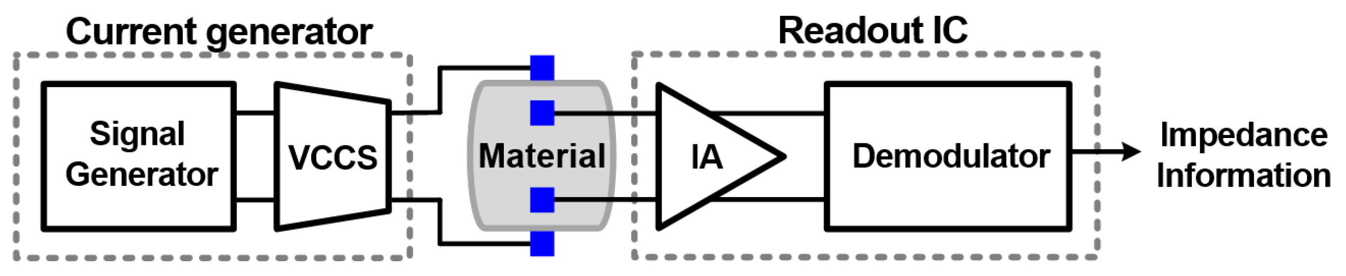
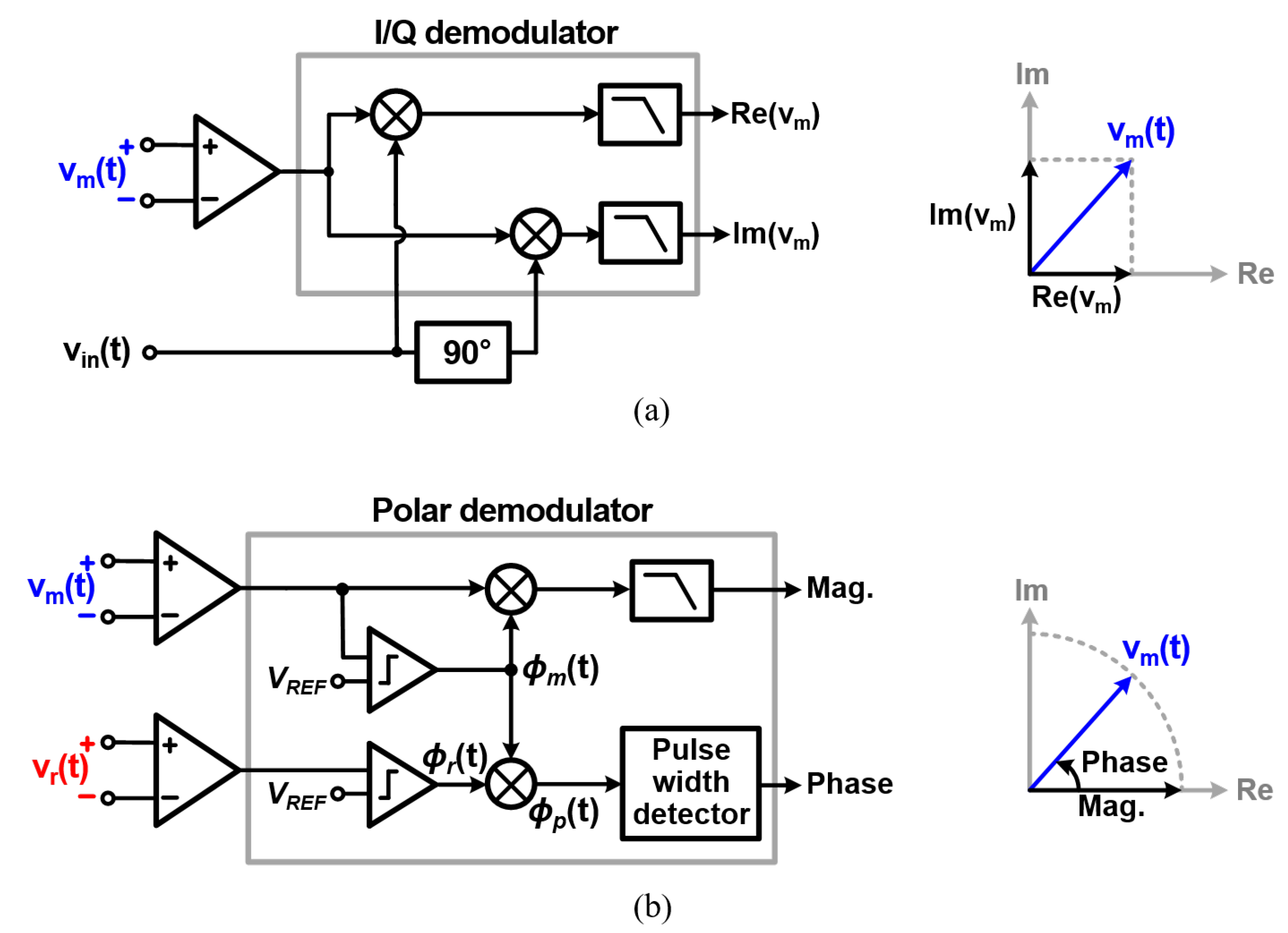
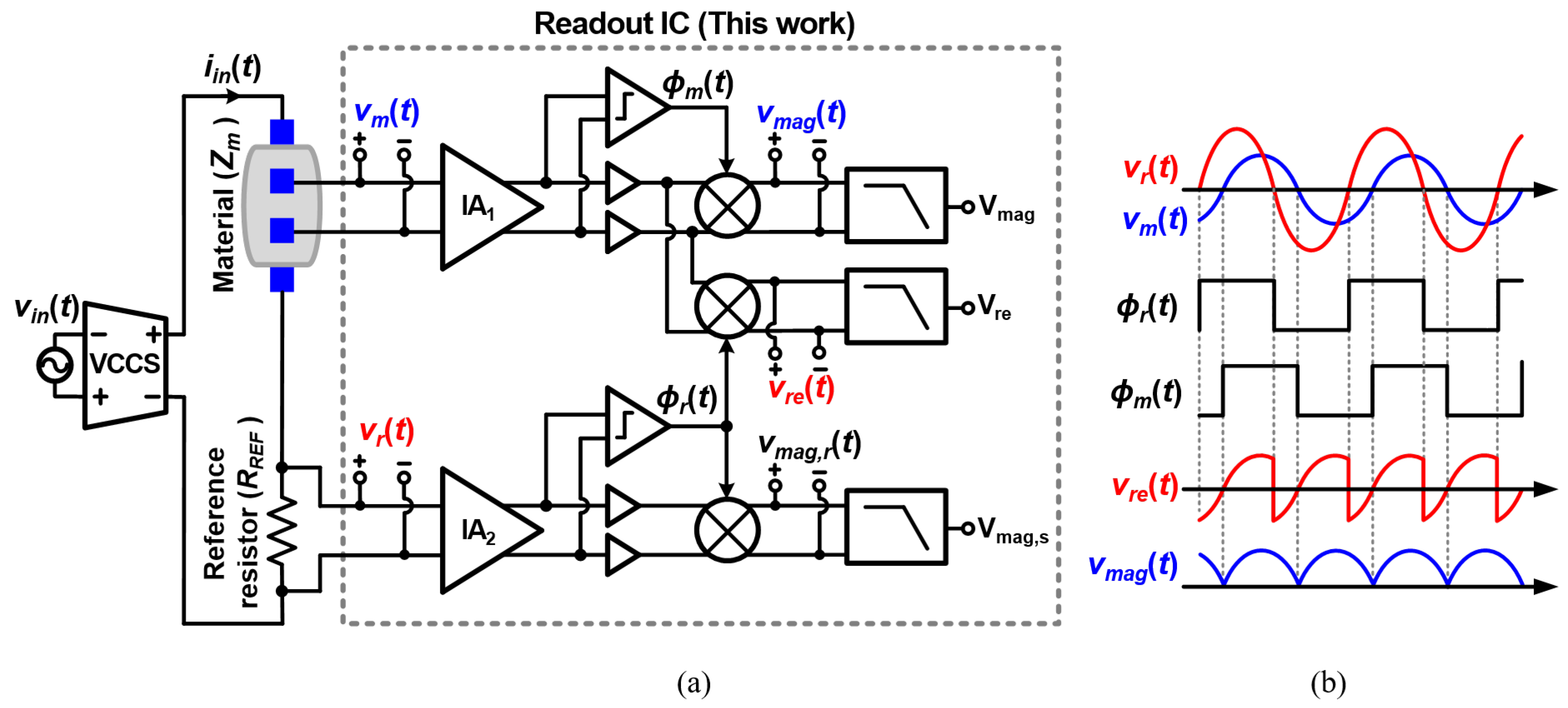
2. Proposed Architecture
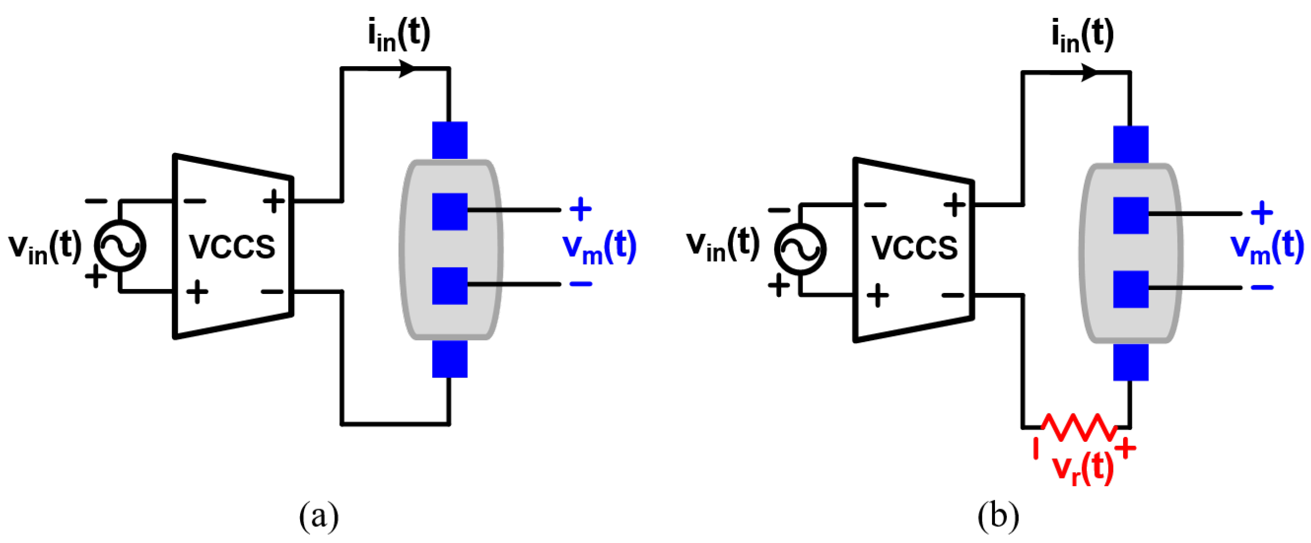
2.1. Magnitude Measurement Path
2.2. Real-Component Measurement Path
3. Circuit Implementation
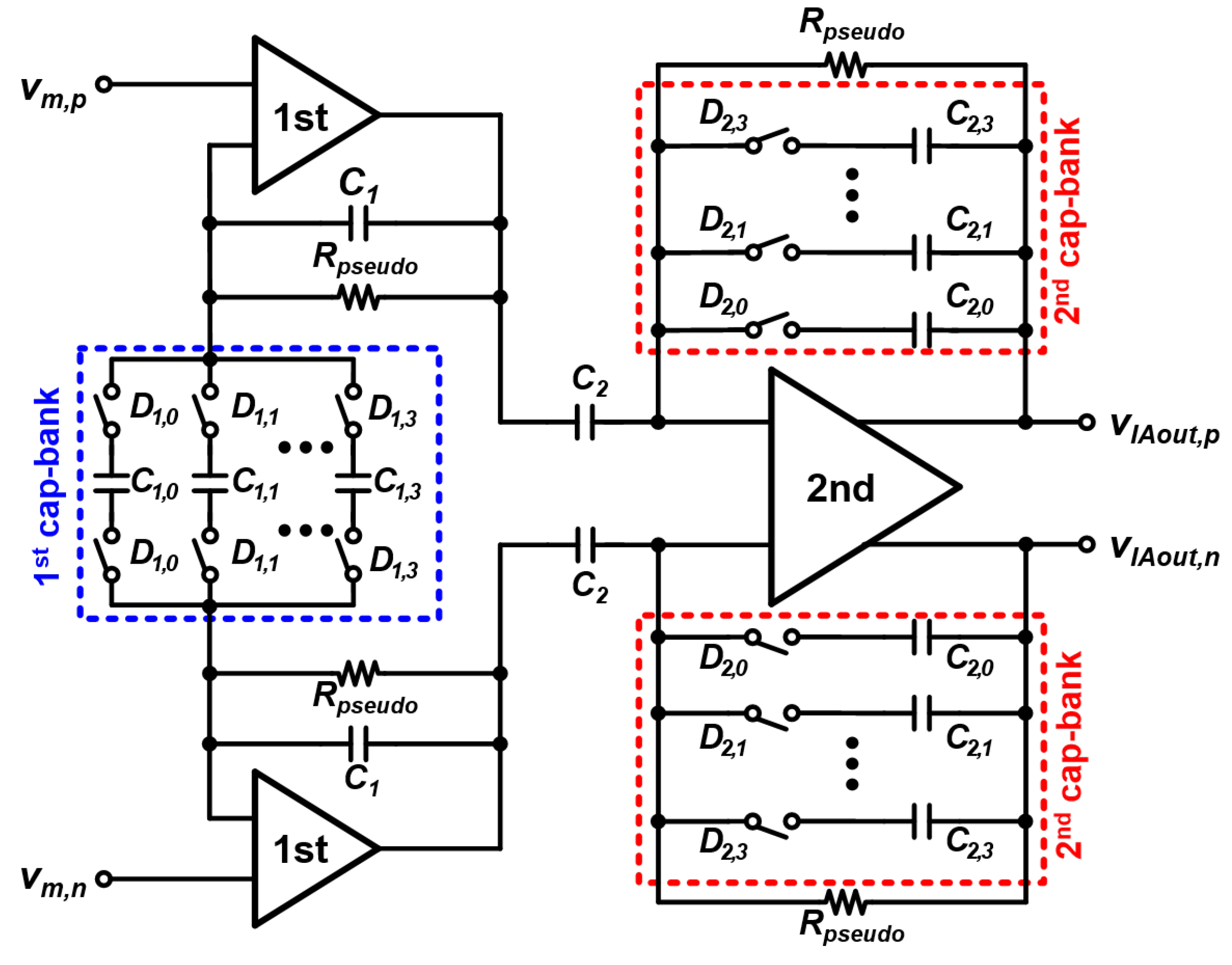
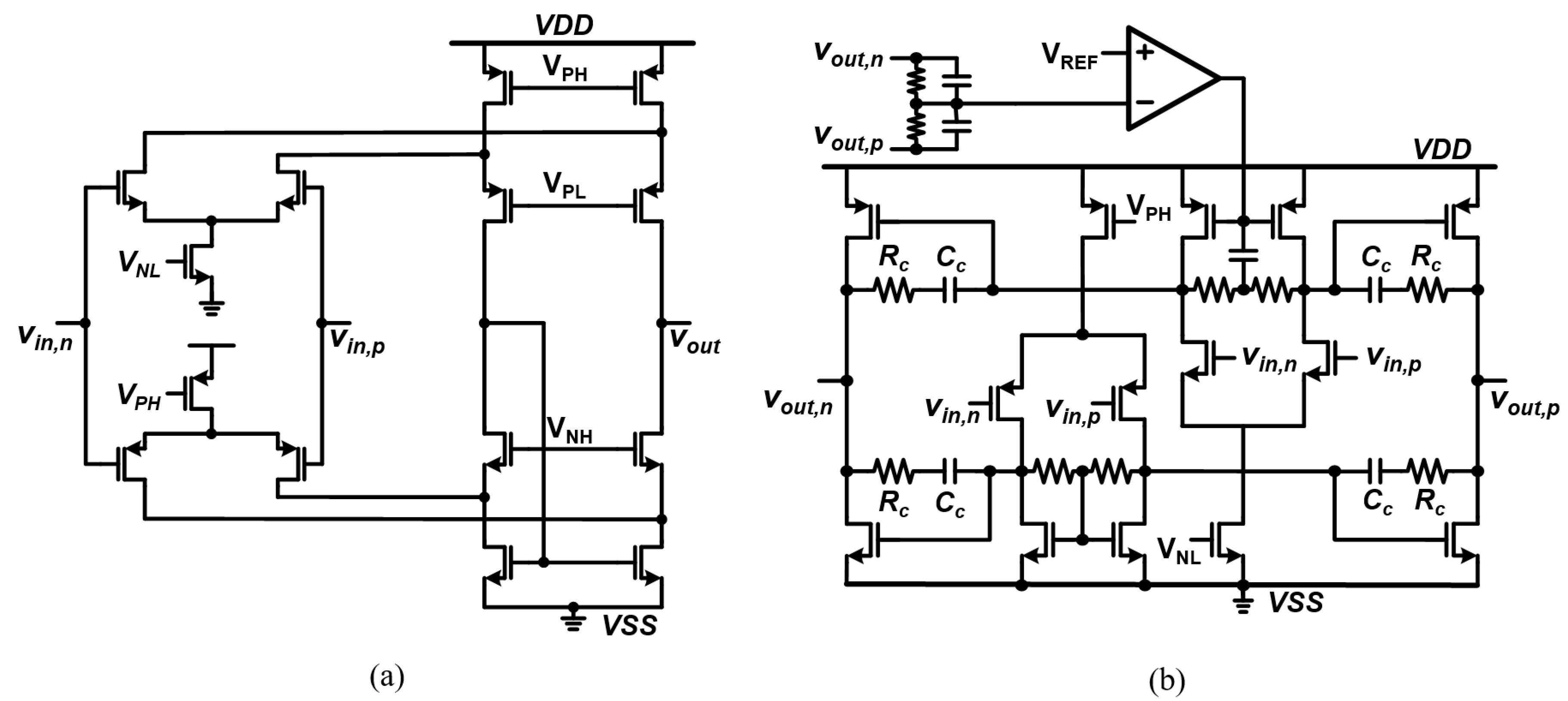
3.1. Instrumentation Amplifier
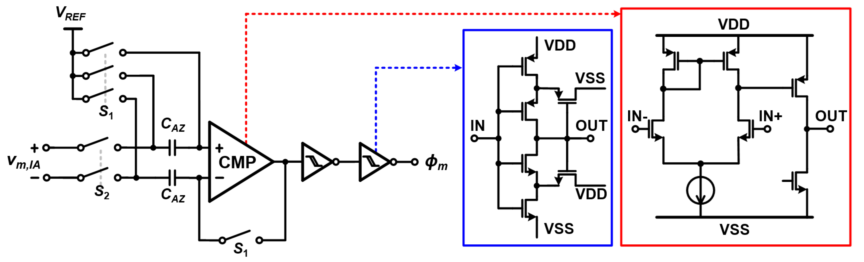
3.2. Comparator
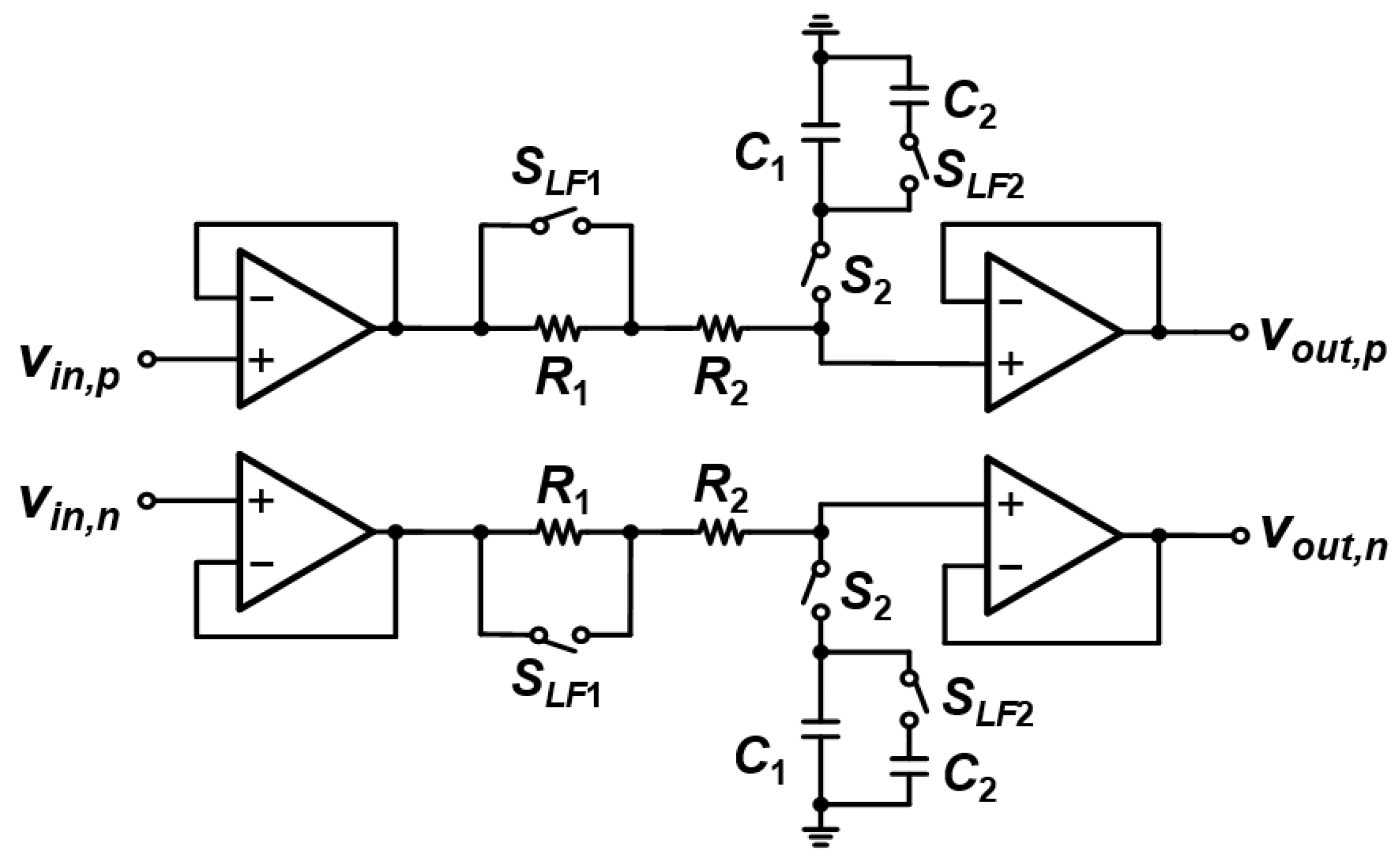
3.3. Low-Pass Filter
4. Results
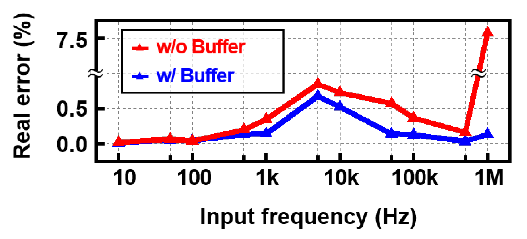
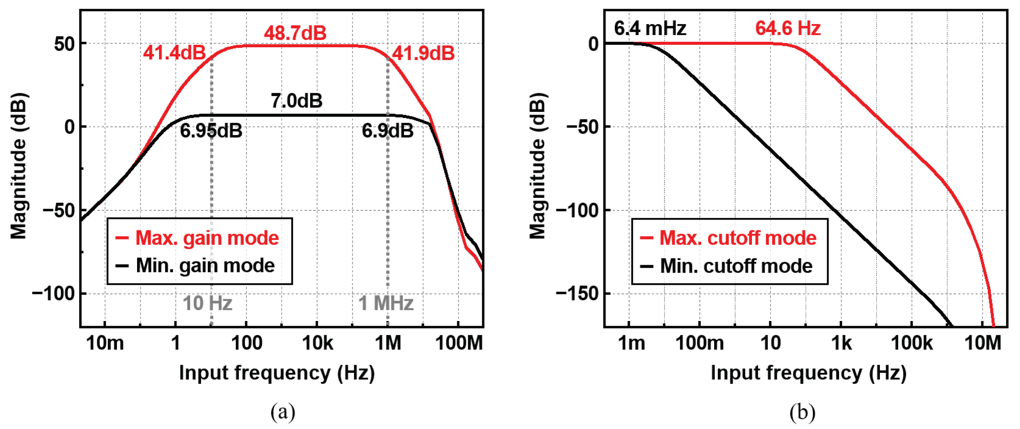
4.1. IA and LPF
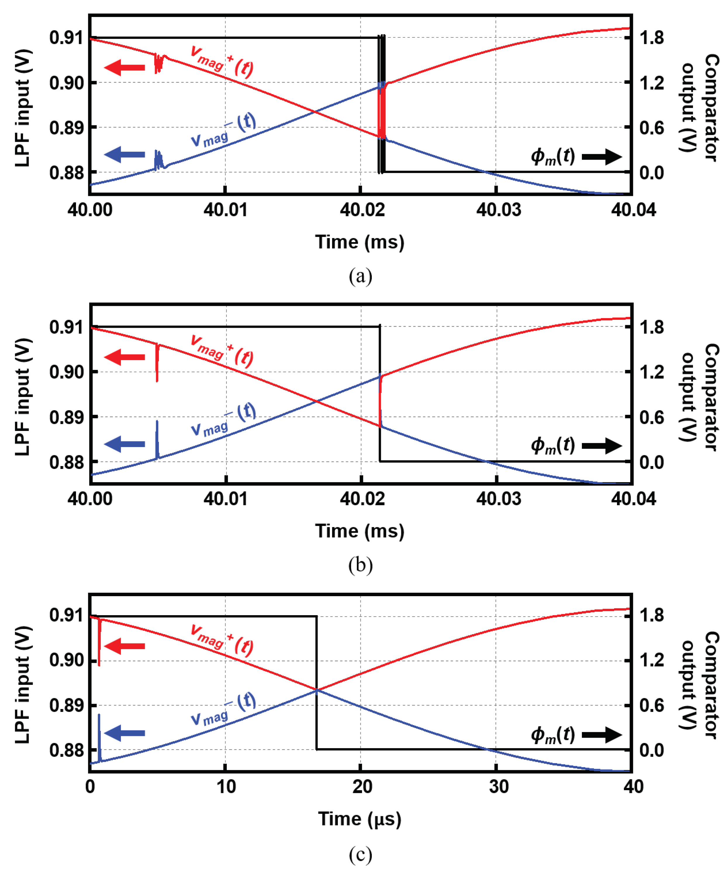
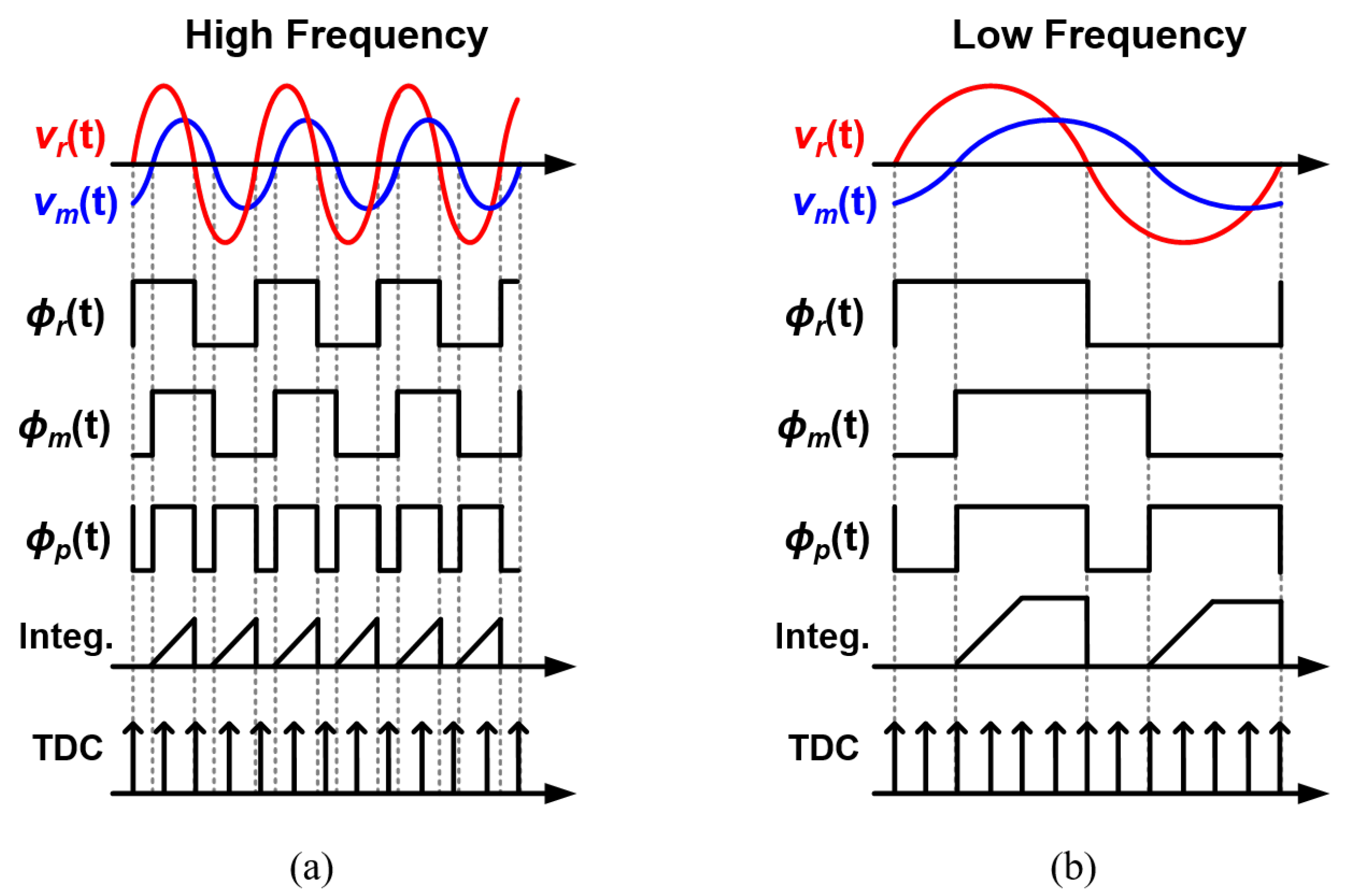
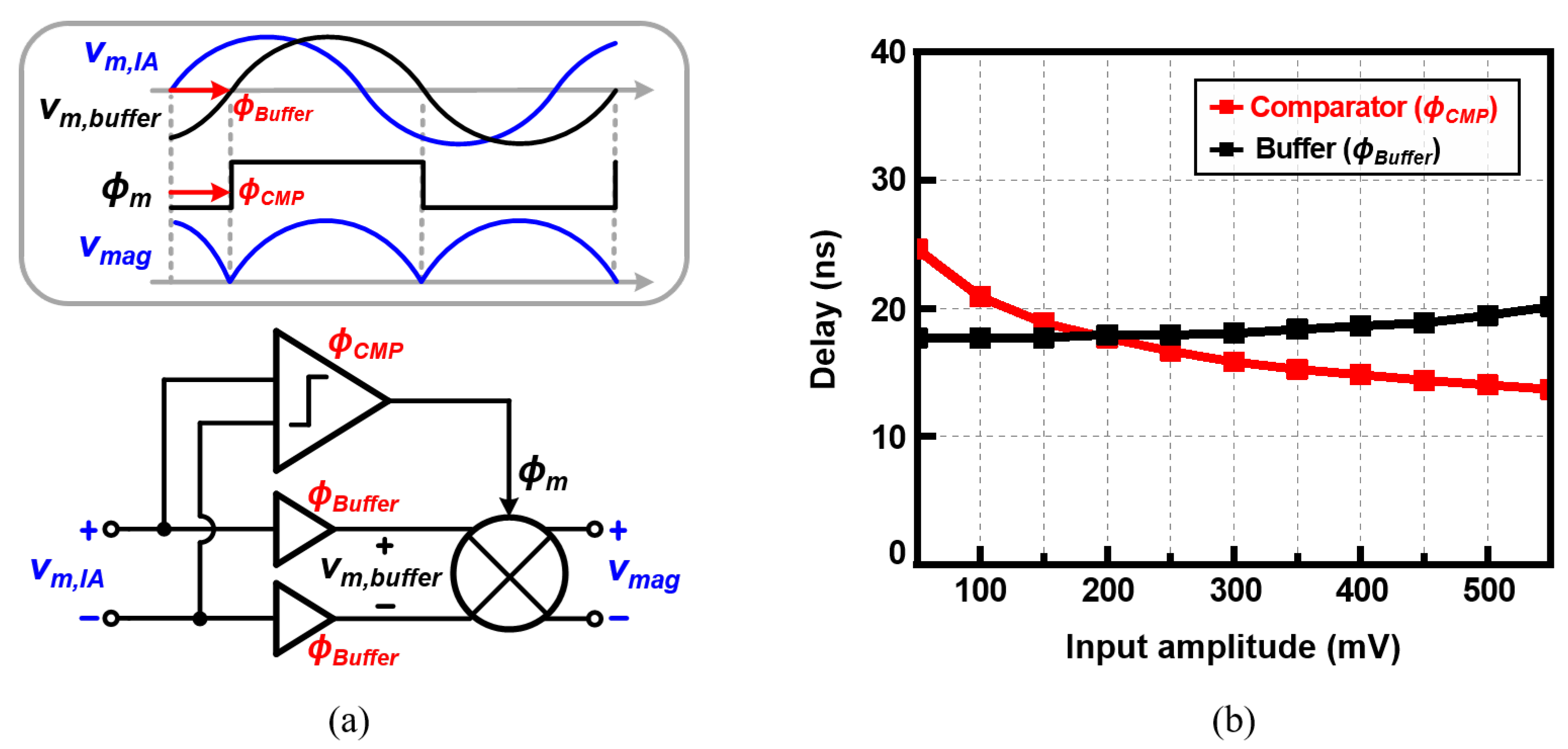
4.2. Chopper and Comparator Operation
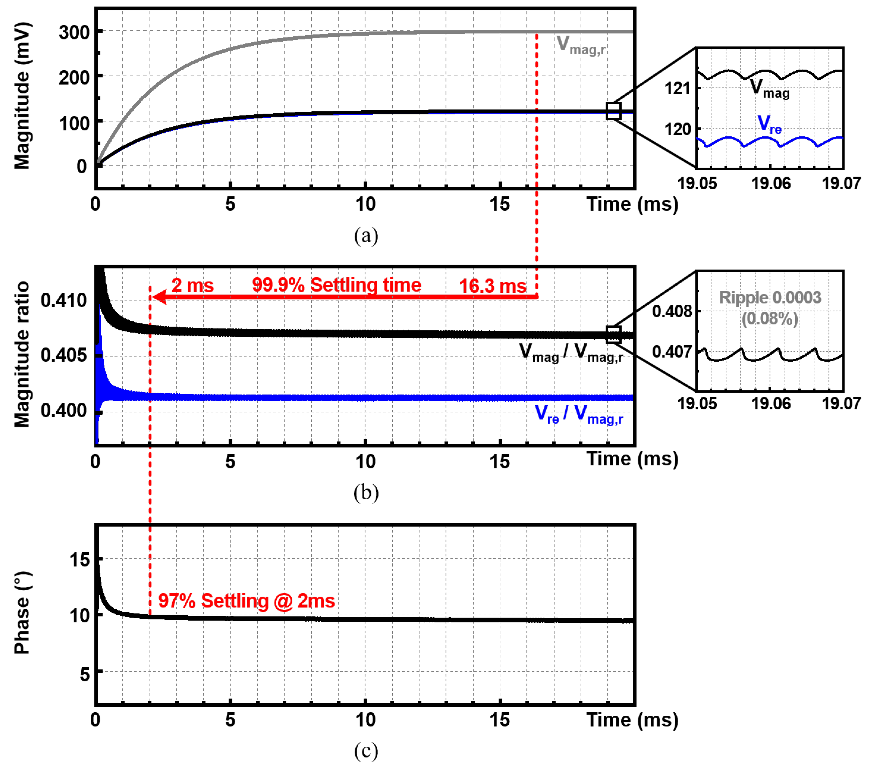
4.3. Settling-Time Reduction
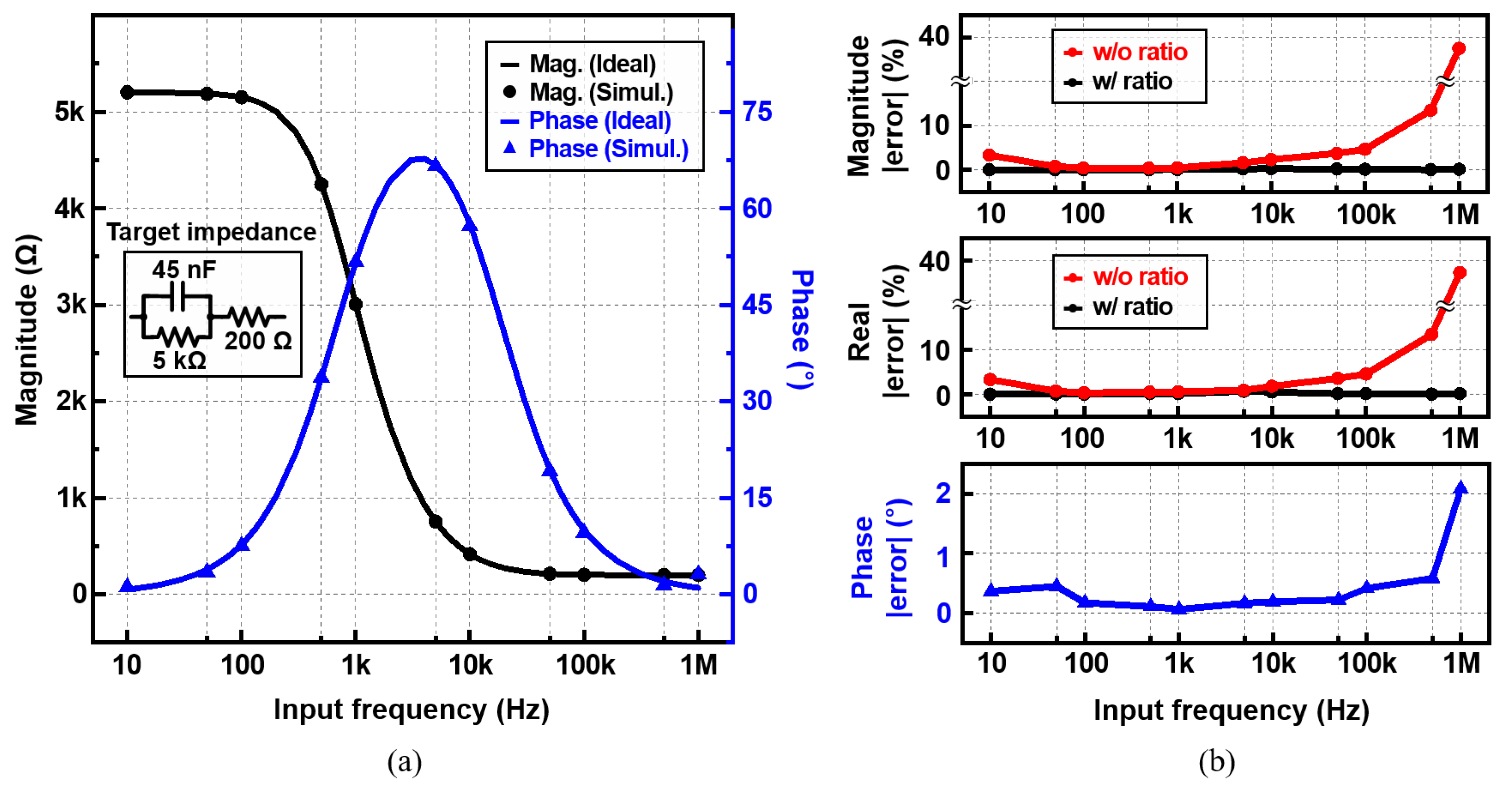
4.4. Impedance Readout Resuylts
4.5. Performance Summary and Comparison
5. Conclusions
Author Contributions
Funding
Acknowledgments
Conflicts of Interest
References
- Ivorra, A.; Gómez, R.; Noguera, N.; Villa, R.; Sola, A.; Palacios, L.; Hotter, G.; Aguiló, J. Minimally invasive silicon probe for electrical impedance measurements in small animals. Biosens. Bioelectron. 2003, 19, 391–399. [Google Scholar] [CrossRef]
- Yufera, A.; Rueda, A.; Munoz, J.M.; Doldan, R.; Leger, G.; Rodriguez-Villegas, E.O. A tissue impedance measurement chip for myocardial ischemia detection. IEEE Trans. Circuits Syst. I Reg. Pap. 2005, 52, 2620–2628. [Google Scholar] [CrossRef] [Green Version]
- Mellert, F.; Winkler, K.; Schneider, C.; Dudykevych, T.; Welz, A.; Osypka, M.; Gersing, E.; Preusse, C.J. Detection of (Reversible) Myocardial Ischemic Injury by Means of Electrical Bioimpedance. IEEE Trans. Biomed. Eng. 2011, 58, 1511–1518. [Google Scholar] [CrossRef] [PubMed]
- Shokrekhodaei, M.; Quinones, S. Review of Non-Invasive Glucose Sensing Techniques: Optical, Electrical and Breath Acetone. Sensors 2020, 20, 1251. [Google Scholar] [CrossRef] [Green Version]
- Liu, B.; Wang, G.; Li, Y.; Zeng, L.; Li, H.; Gao, Y.; Ma, Y.; Lian, Y.; Heng, C.H. A 13-Channel 1.53-mW 11.28-mm2 Electrical Impedance Tomography SoC Based on Frequency Division Multiplexing for Lung Physiological Imaging. IEEE Trans. Biomed. Circuits Syst. 2019, 13, 938–949. [Google Scholar] [CrossRef]
- Kim, M.; Jang, J.; Kim, H.; Lee, J.; Lee, J.; Lee, J.; Lee, K.; Kim, K.; Lee, Y.; Lee, K.J.; et al. A 1.4-m Ω-Sensitivity 94-dB Dynamic-Range Electrical Impedance Tomography SoC and 48-Channel Hub-SoC for 3-D Lung Ventilation Monitoring System. IEEE J. Solid-State Circuits 2017, 52, 2829–2842. [Google Scholar] [CrossRef]
- Mazhab-Jafari, H.; Soleymani, L.; Genov, R. 16-channel CMOS impedance spectroscopy DNA analyzer with dual-slope multiplying ADCs. IEEE Trans. Biomed. Circuits Syst. 2012, 6, 468–478. [Google Scholar] [CrossRef]
- Añorga, L.; Rebollo, A.; Herrán, J.; Arana, S.; Bandrés, E.; Garcia-Foncillas, J. Development of a DNA Microelectrochemical Biosensor for CEACAM5 Detection. IEEE Sens. J. 2010, 10, 1368–1374. [Google Scholar] [CrossRef]
- Liu, H.; Malhotra, R.; Peczuh, M.W.; Rusling, J.F. Electrochemical Immunosensors for Antibodies to Peanut Allergen Ara h2 Using Gold Nanoparticle—Peptide Films. Anal. Chem. 2010, 82, 5865–5871. [Google Scholar] [CrossRef] [Green Version]
- Chiriacò, M.S.; Parlangeli, I.; Sirsi, F.; Poltronieri, P.; Primiceri, E. Impedance Sensing Platform for Detection of the Food Pathogen Listeria monocytogenes. Electronics 2018, 7, 347. [Google Scholar] [CrossRef] [Green Version]
- Olarte, J.; Martínez de Ilarduya, J.; Zulueta, E.; Ferret, R.; Fernández-Gámiz, U.; Lopez-Guede, J.M. A Battery Management System with EIS Monitoring of Life Expectancy for Lead—Acid Batteries. Electronics 2021, 10, 1228. [Google Scholar] [CrossRef]
- Zhang, T.; Jeong, Y.; Park, D.; Oh, T. Performance Evaluation of Multiple Electrodes Based Electrical Impedance Spectroscopic Probe for Screening of Cervical Intraepithelial Neoplasia. Electronics 2021, 10, 1933. [Google Scholar] [CrossRef]
- Halter, R.J.; Hartov, A.; Heaney, J.A.; Paulsen, K.D.; Schned, A.R. Electrical Impedance Spectroscopy of the Human Prostate. IEEE Trans. Biomed. Eng. 2007, 54, 1321–1327. [Google Scholar] [CrossRef]
- Wan, Y.; Borsic, A.; Heaney, J.; Seigne, J.; Schned, A.; Baker, M.; Wason, S.; Hartov, A.; Halter, R. Transrectal electrical impedance tomography of the prostate: Spatially coregistered pathological findings for prostate cancer detection. Med. Phys. 2013, 40, 063102. [Google Scholar] [CrossRef] [PubMed] [Green Version]
- Aberg, P.; Nicander, I.; Hansson, J.; Geladi, P.; Holmgren, U.; Ollmar, S. Skin cancer identification using multifrequency electrical impedance-a potential screening tool. IEEE Trans. Biomed. Eng. 2004, 51, 2097–2102. [Google Scholar] [CrossRef]
- Pathiraja, A.; Ziprin, P.; Shiraz, A.; Mirnezami, R.; Tizzard, A.; Brown, B.; Demosthenous, A.; Bayford, R. Detecting colorectal cancer using electrical impedance spectroscopy: Anex vivofeasibility study. Phys. Meas. 2017, 38, 1278–1288. [Google Scholar] [CrossRef]
- Hong, S.; Lee, K.; Ha, U.; Kim, H.; Lee, Y.; Kim, Y.; Yoo, H.J. A 4.9 mΩ-Sensitivity Mobile Electrical Impedance Tomography IC for Early Breast-Cancer Detection System. IEEE J. Solid-State Circuits 2015, 50, 245–257. [Google Scholar] [CrossRef]
- Zou, Y.; Guo, Z. A review of electrical impedance techniques for breast cancer detection. Med. Eng. Phys. 2003, 25, 79–90. [Google Scholar] [CrossRef]
- Subhan, S.; Ha, S. A Harmonic Error Cancellation Method for Accurate Clock-Based Electrochemical Impedance Spectroscopy. IEEE Trans. Biomed. Circuits Syst. 2019, 13, 710–724. [Google Scholar] [CrossRef]
- Lee, J.; Gweon, S.; Lee, K.; Um, S.; Lee, K.R.; Yoo, H.J. A 9.6-mW/Ch 10-MHz Wide-Bandwidth Electrical Impedance Tomography IC With Accurate Phase Compensation for Early Breast Cancer Detection. IEEE J. Solid-State Circuits 2021, 56, 887–898. [Google Scholar] [CrossRef]
- Khalil, S.F.; Mohktar, M.S.; Ibrahim, F. The Theory and Fundamentals of Bioimpedance Analysis in Clinical Status Monitoring and Diagnosis of Diseases. Sensors 2014, 14, 10895–10928. [Google Scholar] [CrossRef] [PubMed]
- Yan, L.; Bae, J.; Lee, S.; Roh, T.; Song, K.; Yoo, H. A 3.9 mW 25-Electrode Reconfigured Sensor for Wearable Cardiac Monitoring System. IEEE J. Solid-State Circuits 2011, 46, 353–364. [Google Scholar] [CrossRef] [Green Version]
- Song, K.; Ha, U.; Park, S.; Bae, J.; Yoo, H. An Impedance and Multi-Wavelength Near-Infrared Spectroscopy IC for Non-Invasive Blood Glucose Estimation. IEEE J. Solid-State Circuits 2015, 50, 1025–1037. [Google Scholar] [CrossRef]
- Kassanos, P.; Triantis, I.F.; Demosthenous, A. A CMOS Magnitude/Phase Measurement Chip for Impedance Spectroscopy. IEEE Sensors J. 2013, 13, 2229–2236. [Google Scholar] [CrossRef]
- Kassanos, P.; Constantinou, L.; Triantis, I.F.; Demosthenous, A. An Integrated Analog Readout for Multi-Frequency Bioimpedance Measurements. IEEE Sensors J. 2014, 14, 2792–2800. [Google Scholar] [CrossRef]
- Triantis, I.F.; Demosthenous, A.; Rahal, M.; Hong, H.; Bayford, R. A multi-frequency bioimpedance measurement ASIC for electrical impedance tomography. In Proceedings of the 2011 ESSCIRC (ESSCIRC), Helsinki, Finland, 12–16 September 2011; pp. 331–334. [Google Scholar] [CrossRef]
- Analog Devices, Norwood, MA, USA. Datasheet, AD5933, 1 MSPS, 12-Bit Impedance Converter, Network Analyzer. 2013. Available online: http://www.analog.com/media/en/technical-documentation/data-sheets/AD5933.pdf (accessed on 31 December 2021).
- Murphy, D.; Darabi, H.; Abidi, A.; Hafez, A.A.; Mirzaei, A.; Mikhemar, M.; Chang, M.F. A Blocker-Tolerant, Noise-Cancelling Receiver Suitable for Wideband Wireless Applications. IEEE J. Solid-State Circuits 2012, 47, 2943–2963. [Google Scholar] [CrossRef]
- Xu, Y.; Yan, Z.; Han, B.; Dong, F. An FPGA-Based Multifrequency EIT System With Reference Signal Measurement. IEEE Trans. Instr. Meas. 2021, 70, 1–10. [Google Scholar] [CrossRef]
- Asoodeh, A.; Atarodi, M. A Full 360∘ Vector-Sum Phase Shifter with Very Low RMS Phase Error Over a Wide Bandwidth. IEEE Trans. Microwave Theory Tech. 2012, 60, 1626–1634. [Google Scholar] [CrossRef]
- Ibrahim, B.; Hall, D.A.; Jafari, R. Bio-impedance spectroscopy (BIS) measurement system for wearable devices. In Proceedings of the 2017 IEEE Biomedical Circuits and Systems Conference (BioCAS), Turin, Italy, 19–21 October 2017; pp. 1–4. [Google Scholar] [CrossRef]
- Kweon, S.J.; Shin, S.; Park, J.H.; Suh, J.H.; Yoo, H.J. A CMOS Low-Power Polar Demodulator for Electrical Bioimpedance Spectroscopy Using Adaptive Self-Sampling Schemes. In Proceedings of the 2016 IEEE Biomedical Circuits and Systems Conference (BioCAS), Shanghai, China, 17–19 October 2016; pp. 284–287. [Google Scholar] [CrossRef]
- Kweon, S.; Park, J.; Shin, S.; Yoo, H. A low-power polar demodulator for impedance spectroscopy based on a novel sampling scheme. In Proceedings of the 2015 International SoC Design Conference (ISOCC), Gyeongju, Korea, 2–5 November 2015; pp. 331–332. [Google Scholar] [CrossRef]
- Huang, H.; Palermo, S. A TDC-Based Front-End for Rapid Impedance Spectroscopy. In Proceedings of the 2013 IEEE 56th International Midwest Symposium on Circuits and Systems (MWSCAS), Columbus, OH, USA, 4–7 August 2013; pp. 169–172. [Google Scholar] [CrossRef]
- Wu, Y.; Jiang, D.; Habibollahi, M.; Almarri, N.; Demosthenous, A. Time Stamp–A Novel Time-to-Digital Demodulation Method for Bioimpedance Implant Applications. IEEE Trans. Biomed. Circuits Syst. 2020, 14, 997–1007. [Google Scholar] [CrossRef]
- Shin, S.; Jung, Y.; Kweon, S.J.; Lee, E.; Park, J.H.; Kim, J.; Yoo, H.J.; Je, M. Design of Reconfigurable Time-to-Digital Converter Based on Cascaded Time Interpolators for Electrical Impedance Spectroscopy. Sensors 2020, 20, 1889. [Google Scholar] [CrossRef] [Green Version]
- Kweon, S.J.; Park, J.H.; Shin, S.; Yoo, S.S.; Yoo, H.J. A reconfigurable time-to-digital converter based on time stretcher and chain-delay-line for electrical bioimpedance spectroscopy. In Proceedings of the 2017 IEEE 60th International Midwest Symposium on Circuits and Systems (MWSCAS), Boston, MA, USA, 6–9 August 2017; pp. 1037–1040. [Google Scholar] [CrossRef]
- Cheon, S.I.; Kweon, S.J.; Kim, Y.; Koo, J.; Ha, S.; Je, M. A Polar-demodulation-based Impedance-measurement IC Using Frequency-shift Technique with Low Power Consumption and Wide Frequency Range. IEEE Trans. Biomed. Circuits Syst. 2021. [Google Scholar] [CrossRef] [PubMed]


| Parameters | AD5933 [27] | IEEE Sensors 2013 [24] | IEEE BioCAS 2016 [32] | ISOCC 2015 [33] | IEEE MWSCAS 2013 [34] | IEEE TBCAS 2020 [35] | This Work |
|---|---|---|---|---|---|---|---|
| Architecture | I/Q | Polar | Polar | Polar | Polar | Time Stamp | Real/Mag |
| Phase detection method | − | Integrator | TDC | TDC | TDC | TDC | LPF |
| Process (m) | − | 0.35 | 0.25 | 0.18 | 0.18 | 0.18 | 0.18 |
| Supply voltage (V) | 3.3 | ±2.5 | 2.5 | 1.8 | ±0.9 | ±1.65 | 1.8 |
| Power consumption (mW) | 33.0 | 21.0 | 10.3 | 10.0 | 28.0 | 0.684 | 0.513 |
| Frequency range (Hz) | 1–100 k | 100–100 k | 1 k–2.048 M | 100–100 k | 100–10 M | 10–500 k | 10–1 M |
| Magnitude error (%) | <2 | <3.5 | <1.0 | <1.9 | <2.5 | <2.94 | <0.3 |
| Phase () | <0.9 | <3.6 | <1.3 | <0.2 | <2.2 | <1.19 | <0.6 (500 kHz) <2.1 (1 MHz) |
Publisher’s Note: MDPI stays neutral with regard to jurisdictional claims in published maps and institutional affiliations. |
© 2022 by the authors. Licensee MDPI, Basel, Switzerland. This article is an open access article distributed under the terms and conditions of the Creative Commons Attribution (CC BY) license (https://creativecommons.org/licenses/by/4.0/).
Share and Cite
Cheon, S.-I.; Kweon, S.-J.; Kim, Y.; Koo, J.; Ha, S.; Je, M. An Impedance Readout IC with Ratio-Based Measurement Techniques for Electrical Impedance Spectroscopy. Sensors 2022, 22, 1563. https://doi.org/10.3390/s22041563
Cheon S-I, Kweon S-J, Kim Y, Koo J, Ha S, Je M. An Impedance Readout IC with Ratio-Based Measurement Techniques for Electrical Impedance Spectroscopy. Sensors. 2022; 22(4):1563. https://doi.org/10.3390/s22041563
Chicago/Turabian StyleCheon, Song-I, Soon-Jae Kweon, Youngin Kim, Jimin Koo, Sohmyung Ha, and Minkyu Je. 2022. "An Impedance Readout IC with Ratio-Based Measurement Techniques for Electrical Impedance Spectroscopy" Sensors 22, no. 4: 1563. https://doi.org/10.3390/s22041563
APA StyleCheon, S.-I., Kweon, S.-J., Kim, Y., Koo, J., Ha, S., & Je, M. (2022). An Impedance Readout IC with Ratio-Based Measurement Techniques for Electrical Impedance Spectroscopy. Sensors, 22(4), 1563. https://doi.org/10.3390/s22041563