Abstract
We demonstrate, numerically, a new concept for on-chip magneto-optical (MO) modulation in dense wavelength division multiplexing (DWDM) applications. Our idea uses materials and mechanisms that are compatible with current silicon-on-insulator fabrication and CMOS technologies for monolithic integration. The physics behind our idea stems in the exploitation of the enhanced MO activity of a micro-ring, made of cerium substituted yttrium iron garnet (Ce:YIG) material, to actively manipulate the resonance wavelengths of an adjacent micro-ring resonator (MRR) of silicon (Si). This active manipulation of the latter MO-MRR structure is used to modulate the optical signal traveling through a side-coupled Si bus waveguide. Moreover, by proper tailoring multiple MO-MRRs (side-coupled to the single Si bus waveguide) to match wavelength channels in DWDM across the entire C-band optical communications spectrum, we extend our proposal to massive and dynamic MO modulation in DWDM applications. Significantly, we noticed that the active MO shifting of the resonant wavelength (used for MO modulation here) can be used for improvements in the spectrum utilization efficiency in future elastic optical networks (EONs).
1. Introduction
Owing to the increasing popularity of video streaming, mobile and cloud computing services, data traffic in optical communications networks is experiencing explosive growth during the last few years. This trend seems to be unbroken, at least during the upcoming decade, due to sustained innovations in wireless communications and its seamless integration into existing fibre-optic infrastructures [1,2]. Hence, improvements in the spectrum utilization efficiency of optical transport networks are needed to cope with the associated challenges. Moreover, seamlessly integrated photonic and nano-electronic circuits are required for high-fidelity optical signal processing, which demands monolithic (i.e., on a single chip) integration of photonic circuits into CMOS (complementary metal-oxide semiconductor) technology [3,4].
Current approaches to meet the increasing capacity and bandwidth requirements (in optical communications networks) are mostly based on the use of wavelength division multiplexing (WDM) systems [5,6], where the optical transmission spectrum of a single optical fiber is divided into multiple channels of non-overlapping wavelengths. Importantly, each single communication channel can operate at whatever speed it desires by exploiting the complementary physics between electronic and photonic technologies [7]. This level of integrability (at the chip scale) is reached through the silicon-on-insulator (SOI) micro-ring resonators (MRRs), which are essential building blocks for channel add/drop filters [8,9,10], interleavers [11], and multiplexing/demultiplexing devices [12] in advanced optical communications networks. In particular, sharp optical resonances associated to MRRs are used to add/extract specific wavelengths without disturbing other channels in WDM. Furthermore, the CMOS compatibility of SOI technology enables high-density integration of photonic-to-electronic functions on a chip [3,4]. However, in spite of these advantages, the spectrum utilization efficiency of WDM is still limited by the fixed channel and grid spacing from conventional approaches.
On the other hand, to continue scaling optical communications networks, both in density and complexity, it is necessary to replace the conventional metallic intra- and inter-chip data links (limited by losses, bandwidth, and crosstalk) with their optical counterparts [13,14,15,16]. The workhorse of an optical interconnect is the optical modulator, i.e., the device used to load information onto the light beam [17,18,19,20]. According to the physical principle, modulators can be classified as electro-optical (EO) [21], thermo-optical (TO) [22] and, more recently, magneto-optical (MO) [23,24,25]. In EO modulation, for example, an external electric field is used for dynamic manipulation of the guided light intensity and phase [3,26]. Although recent EO modulation devices exploit the unique properties of advanced materials (e.g., graphene) to improve the energy and modulation performances [27,28,29], their operation speeds are still considered limited [30]. In the case of TO modulators, the features of the optical signal are manipulated by temperature changes (induced through the thermoelectric effect) [22]. However, this latter modulation mechanism results in vulnerable optical circuits (susceptible to thermal fluctuations) and additional complexity (in terms of design and components) for temperature stabilization [31]. The MO approach, in contrast, employs an external magnetic field for optical signal modulation. This last approach overcomes the limitations associated to EO and TO modulation mechanisms [32,33]. Nevertheless, current MO modulation approaches are based in the polarization conversion effect, via the MO Faraday effect, which can introduce unwanted noise and impair optical-to-electronic (electronic-to-optical) coupling.
In this work, we numerically demonstrate a new concept for MO modulation and/or dynamic WDM applications. MO activity is introduced using the cerium substituted yttrium iron garnet (Ce:YIG) material, which has recently been monolithically integrated (through both SOI and CMOS compatibility) into broadband optical isolators [34,35] and non-volatile MO switches [36]. Furthermore, a Si-based MRR, with an inner Ce:YIG MO disk, was recently used for dynamic add/dropping of modes between two coupled waveguides [37]. To develop our idea, we first use a single racetrack-like MO-MRR, side-coupled to a single Si-waveguide, to demonstrate a concept for amplitude-based MO modulation, i.e., without polarization conversion of the optical signal. The MO-MRR is built by two adjacent and concentric micro-rings. The external micro-ring is made of Si to provide the corresponding resonances on the guided modes, whereas the inner micro-ring made of Ce:YIG for MO modulation of the Si micro-ring resonances. Second, we use a linear array of MO-MRRs side-coupled to a single bus waveguide for massive modulation on a single chip. More specifically, we show that this last structure can be used for dynamically tunable dense WDM (DWDM) along the optical C-band (1530 nm up to 1565 nm), with a free spectral range (FSR) of 100 GHz. Finally, it is worth mentioning that the modulation mechanism shown here reaches extinction ratios (ERs) in the order of 46 dB which, as shown comparatively herein, are higher than all previous modulation approaches.
2. Theory and Modeling
Figure 1a,b show a three-dimensional (3D) view and an upper view of the proposed design. The MO-MRR is formed by two adjacent and concentric micro-rings with a racetrack shape and side-coupled to a straight waveguide. The external MRR and the straight waveguide are both composed of Si, whilst the inner micro-ring is made of MO Ce:YIG material. The high-refractive-index contrast of Si provides waveguiding of the optical signals in the structures, whereas the Ce:YIG material is used for MO modulation of the resonant wavelengths in the external Si-MRR. The substrate is considered of silica (SiO2), which is compatible with SOI and CMOS technologies. The Si waveguide and MRR are considered with the same width and height H, whilst the inner Ce:YIG micro-ring has width and height H. The inner radius of the Ce:YIG micro-ring semicircular sections is denoted by R (see Figure 1), whilst the straight waveguide section has length A. The gap between the Si-MRR and the Si-waveguide is denoted by G. The system in Figure 1 can be monolithically integrated through the use of pulsed laser deposition (PLD) [34,38], nanolithography [39], or a proper combination of these and other methods for growing materials. Moreover, although magnetic fields can be applied at the chip-scale using integrated Si-compatible electromagnetic coils, as recently demonstrated [36], results in this work were obtained using the intrinsic magnetization of the CeYIG material (at magnetization saturation level).
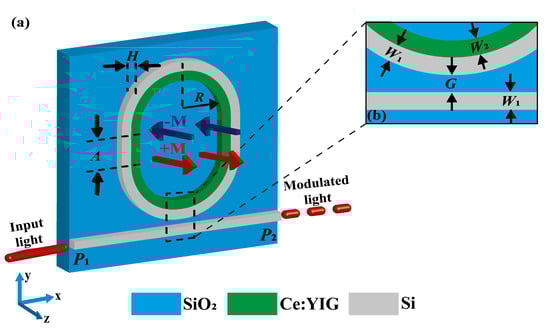
Figure 1.
(a) Schematic 3D of the MO-MRR and (b) a zoom-in of the highlighted region in (a).
The input signal in the system is applied through the port 1 () and propagates to the port 2 (), as illustrated in Figure 1a. As it is well-known from the available literature [40], under the phase-matching condition, the guided optical mode in the Si-waveguide is resonantly coupled to the Si-MRR. This phase-matching condition states that resonances occur when the wavelength of the optical beam fits a whole number of times inside the optical length of the ring. Then, the system exhibits a set of resonances described by [40,41]
where is the resonance wavelength, is the effective refractive index of the guided mode, L is the optical path along the ring and is an integer that defines the multiple of the wavelength that characterizes the resonance. Since we are considering MO activity in the proposed device, the superscript ± is used to indicate the magnetization () sense along the magnetized axis (z-axis in this case, as illustrated in Figure 1a), i.e., and depend on the magnetization sense in the structure.
MO effects can induce phase, polarization, and/or amplitude changes in the optical field depending on the magnetization configuration in the system [42]. In particular, MO activity only induces amplitude changes on the optical mode when the magnetization is parallel to the magnetic field component of light. Therefore, we restrict, here, our analysis to the case of guided modes with their magnetic field component along the z-axis, i.e., parallel to magnetization of Ce:YIG illustrated in Figure 1a. The anisotropic permittivity of Ce:YIG for this configuration is represented by the permittivity tensor
where represents the isotropic diagonal permittivity component of Ce:YIG, is used for pointing along the direction, and are the anisotropic off-diagonal components. The values of and are used from the experimental measurements in Ref. [43]. For simplicity, calculations are made within the magnetic saturation condition, which requires magnetic field amplitudes of ∼2 kOe [43]. On the other hand, the isotropic permittivities of Si and SiO are used from experimental values as [44], [45], respectively. All permittivities are considered constant due to negligible changes ( for the diagonal and for the off-diagonal components) within the working wavelength range.
We optimized the proposed device to work in the fundamental mode, considering that the magnetic field component of the guided wavelength () is along the z-axis. As the current lasers for WDM systems are mostly available to operate around nm [46], we used nm for the geometrical designs of the MO-MRR and straight waveguide. We start the optimization by looking for the lowest insertion loss (IL) on the straight waveguide, i.e., the highest transmittance level at , in the non-resonant condition. Then, we optimized the gap between the straight waveguide and the MO-MRR by searching for the best wave coupling with the lowest IL in the system. Through the corresponding numerical results/analysis, we obtained nm, m, nm, nm, and nm for the geometrical parameters in Figure 1. We should remark here that, to avoid the use of large computational resources and time-consuming calculations, we carried out simulations of a 3D device by using two complementary 2D simulations. First, we calculate the mode effective index for a simplified longitudinal 2D structure (along the xy-plane) with optimized waveguides widths ( and ). Then, using the effective index and widths information, in the second 2D simulation we calculate the waveguides cross-sections to find the corresponding heights. The input port, named , was excited with 1 mW, whereas the output port, named , was used to measure the transmittance (labeled as ), as illustrated. Numerical results were obtained using the finite element method (FEM) with the commercial software COMSOL multi-physics® (Stockholm, Sweden). Calculations as function of the wavelength were swept using steps of nm. The mesh was used with finer sizes of around the waveguides and in the farthest region from the waveguides, with a growth transition rate of 1.1. Moreover, scattering boundary conditions and absorbing perfect matched layers (PMLs) were used to avoid spurious numerical reflections.
3. Results and Discussion
Let us start discussing the MO modulation mechanism. In this case, our attention is focused around the working wavelength nm, within a small wavelength range of the C-band (from 1550 nm to nm), where is calculated as a function of . Numerical results are comparatively shown for (i.e., the demagnetized system) and in Figure 2. The strong resonance at 1550.44 nm (for ) is verified numerically with a very deep transmittance drop dB. For () we note that the transmittance deep suffers a resonance shift of nm ( nm), with a relatively small change ( dB) in the transmittance deep. The symmetric displacement of resonance around the working wavelength, for , totalize a wavelength shift of nm (in the magnetic saturation condition), as indicated in Figure 2. At nm ( nm) the marks I and II (III and IV) indicate the wavelength where our design can work as a MO modulator. Indeed, considering two levels of output intensity, a non-return-to-zero (NRZ) encoded bitstream can be assumed using the magnetization sense along the z-axis, e.g., for bit 1 and for bit 0, as depicted in the inset of Figure 2.
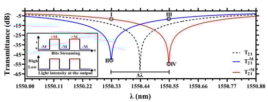
Figure 2.
Transmittances in the MO-MRR for non-magnetized (black dashed curve) and magnetized to (blue solid curve) and (red solid curve). The points I and III symbolize a possible coding for bit 1, whilst the points II and IV may coding the bit 0, as depicted in the inset.
The ER, defined as the difference between the IL and the resonance deep, is as important parameter to measure the modulation performance. Calculating the ER for the proposed structure working at nm ( nm), indicated by points I & II (III & IV) in Figure 2, we obtain dB ( dB). This result is remarkably high in comparison to other recent works, as it is shown in Table 1. Moreover, it can be also noted from the Table 1 that the radius of our proposal is relatively small (with a small footprint of 1723 μm2), enabling high density on-chip integration. The upper view of the magnetic field profiles associated to the modes I & III and II & IV are shown in Figure 3a,b, respectively. For visualization purposes, the region highlighted in Figure 3a is zoomed in Figure 3c. From this last figure we note that the guided mode in the MRR of Si is distributed inside the adjacent micro-ring of Ce:YIG, where stems the physical principle in this work (through the enhanced MO activity of Ce:YIG). A cross-section view of the magnetic field profile in the highlighted region is shown in Figure 3d, where the lower refractive index contrast at the Si-Ce:YIG interface (compared with the Si–air interface) explains the higher evanescent light penetration into the Ce:YIG material.

Table 1.
Features comparison among the optical effects in MRR-based modulators.
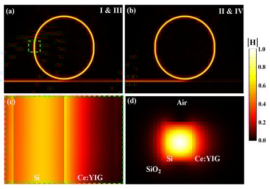
Figure 3.
Normalized H-field in the MO-MRR. (a) The system in non-resonance condition (I & III) and (b) in resonance condition (II & IV). In (c), an inset from (a) at the straight MRR section, where one can see the guided wave and the evanescent field along the MO ring. (d) the cross-section view of the MO-MRR for TM mode.
For practical implementations of our proposal, it becomes necessary for an analysis of the tolerance to fabrication errors. Although several nanolithography techniques have been developed for precise fabrication of MRRs [40,41], due to the high sensitivity of sharp resonances to the micro-ring radius and waveguide dimensions, the sensitivity of MO activity to small manufacturing errors deserves attention in this work. So far, the inner Ce:YIG MRR was optimized to have , which, in turn, produce nearly the same transmittance dips for , as seen in Figure 2, with a slight difference of dB. Figure 4a shows calculations of for the system with , using , whereas results for and are shown in Figure 4b, where solid and dashed curves are used for + and −. These results indicate resonance shifts and increasing difference between the transmittance dips for , except for where a difference as small as 0.4 dB is obtained. Interestingly, a linear dependence of with the ratio was noticed, however, due to the negligible small slope , we can consider as constant, as illustrated by the blue curve in Figure 4c. Additionally, for sake of clarification, the resonance difference in the frequency domain () shows a constant behavior, as it can be observed. Therefore, fabrication errors should not be higher than to guarantee almost the same level of MO activity for .
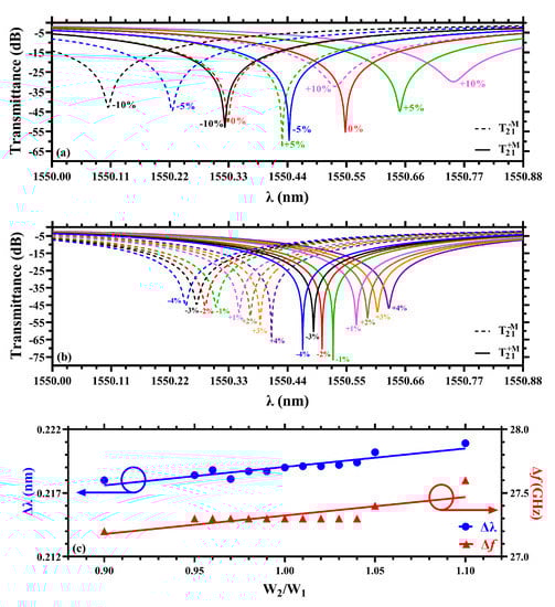
Figure 4.
Resonances for with small differences between the widths and . (a) Variations with steps of % from 0% to % and (b) variation from to % with steps of 1%. (c) A linear fitting of as function of .
On the other hand, our concept can be extended along the entire optical C-band ( nm), for massive MO modulation, by using a bus waveguide side-coupled with a linear arrange of MO-MRRs. A schematic representation of the system is shown in Figure 5a, where the straight waveguide and racetrack-like MO-MRRs are illustrated. Considering that on-chip integrated electromagnets can be manufactured with available fabrication techniques [36,50], we assume that the magnetization sense of each individual MO-MRR can be manipulated at will. This last application, therefore, enables a new concept for magnetically tunable DWDM applications (allowing for a better harnessing of the available optical spectrum), where different wavelength channels can be dynamically accessed/modulated through the use of locally applied magnetic fields. It is worth mentioning that we are working in the state of magnetization saturation for the Ce:YIG material, that is, magnetic fields in the system are of the order of 0.2 T, with MRRs far apart (to avoid any type of coupling). Therefore, after the system is magnetized, the external magnetic field can be turned off to prevent unwanted crosstalk or other effects that the external magnetic field may induce. A major issue to be avoided is cross-talk (CT) among adjacent optical channels, which, in DWDM, are separated by a fixed FSR value of 200 GHz ( nm), 100 GHz ( nm), 50 GHz ( nm), etc., following the International Telecommunication Union (ITU-T) [51]. After numerical analysis, we found that the minimum FSR allowed to avoid CT is nm, i.e., our device can work in DWDM with an GHz. Consequently, we fixed GHz and designed the corresponding MO-MRRs lengths to modulate each one of the 44 different optical channels in the C-band. The corresponding numerical results are shown in Figure 5b–i which, for the sake of presentation, were limited to the wavelength range from 1550 nm to nm. In these latter figures, we use three optical channels labeled (black dotted-line), (green dotted-line), and (red dotted-line), with eight combinations of , to show that each single optical channel can be modulated without interfering on the resonant behavior of the adjacent channels. Importantly, the active manipulation of individual resonant wavelength channels in Figure 5 can be used for future developments in elastic optical networks (EONs) which, in contrast to DWDM, can have a mixture of different FSR values (on an as-needed basis) to provide almost any line rate [5,6].
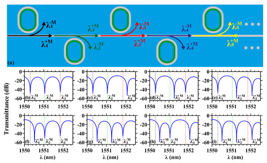
Figure 5.
(a) Schematic representation of multiple MO-MRRs side-coupled to a single Si-waveguide for massive MO modulation in DWDM applications. (b–i) MO modulation in DWDM for different combinations of .
A guide for design of MO-MRRs is given in Table 2, where geometric changes used to provide the different resonances in Figure 5 are shown. In particular, it should be noted that only the straight section of the race-track shape, A, is altered to obtain all the different resonances compatible with the optical carriers in DWDM systems [51]. As noticed, the resonance wavelengths exhibit a linear increasing/decreasing with increasing/decreasing A, which indicates a very simple way to implement this concept. In particular, Figure 5 presents the MO-MRRs with nm, nm, and nm, which are spaced by nm, leading to resonance shifts of around nm (required to reach the GHz).
Table 2.
Length A for each optical channel modulation spaced, for 100 GHz DWDM systems.
4. Conclusions
In summary, we numerically shown a concept for MO modulation based in the use of MO-MRRs. Our results indicate highly efficient modulation of a single wavelength channel (using a single MO-MRR) or multiple individual channels in DWDM applications (using a set of MO-MRRs). Significantly, we considered materials, geometries, and components, that can be monolithically integrated with currently available manufacturing methods. Although we fixed GHz, we noticed from the active resonance shifting that future implementations in EONs are feasible with our idea. In particular, from results for massive MO modulation in DWDM, it can be seen that the active modulation of a specific wavelength channel does not disturb/overlap the other channels in the system. Remarkably, we reached a MO modulation depth of dB which, as comparatively shown, is at least 1.7 times higher than the best result from previous literature.
Author Contributions
Conceptualization, J.V.S.N. and W.O.F.C.; methodology, W.O.F.C.; software, J.V.S.N.; visualization, J.V.S.N.; validation, J.V.S.N., W.O.F.C. and J.R.M.-S.; investigation, J.V.S.N. and W.O.F.C.; writing—original draft preparation, J.V.S.N. and W.O.F.C.; writing—review and editing, J.R.M.-S. All authors have read and agreed to the published version of the manuscript.
Funding
Partial financial support was received from RNP, with resources from MCTIC, Grant No. 01245.010604/2020-14, under the Brazil 6G project of the Radiocommunication Reference Center (Centro de Referência em Radiocomunicações—CRR) of the National Institute of Telecommunications (Instituto Nacional de Telecomunicações—Inatel), Brazil.
Data Availability Statement
Data underlying the results presented in this paper are not publicly available at this time but may be obtained from the authors upon reasonable request.
Acknowledgments
The authors acknowledge the financial support from the Brazilian agencies Coordenação de Aperfeiçoamento de Pessoal de Nível Superior—Brasil (CAPES)—Finance Code 001, the National Council for Scientific and Technological Development-CNPq (314671/2021-8) and FAPESP (2021/06946-0).
Conflicts of Interest
The authors declare no conflict of interest.
References
- Nagatsuma, T.; Ducournau, G.; Renaud, C.C. Advances in terahertz communications accelerated by photonics. Nat. Photonics 2016, 10, 371–379. [Google Scholar] [CrossRef]
- Ummethala, S.; Harter, T.; Koehnle, K.; Li, Z.; Muehlbrandt, S.; Kutuvantavida, Y.; Kemal, J.; Marin-Palomo, P.; Schaefer, J.; Tessmann, A.; et al. THz-to-optical conversion in wireless communications using an ultra-broadband plasmonic modulator. Nat. Photonics 2019, 13, 519–524. [Google Scholar] [CrossRef]
- Reed, G.T.; Mashanovich, G.; Gardes, F.Y.; Thomson, D.J. Silicon optical modulators. Nat. Photonics 2010, 4, 518–526. [Google Scholar] [CrossRef]
- Atabaki, A.H.; Moazeni, S.; Pavanello, F.; Gevorgyan, H.; Notaros, J.; Alloatti, L.; Wade, M.T.; Sun, C.; Kruger, S.A.; Meng, H.; et al. Integrating photonics with silicon nanoelectronics for the next generation of systems on a chip. Nature 2018, 556, 349–354. [Google Scholar] [CrossRef] [PubMed]
- Luo, L.W.; Ophir, N.; Chen, C.P.; Gabrielli, L.H.; Poitras, C.B.; Bergmen, K.; Lipson, M. WDM-compatible mode-division multiplexing on a silicon chip. Nat. Commun. 2014, 5, 3069. [Google Scholar] [CrossRef]
- Wang, X.; Kuang, K.; Wang, S.; Xu, S.; Liu, H.; Liu, G.N. Dynamic routing and spectrum allocation in elastic optical networks with mixed line rates. J. Opt. Commun. Netw. 2014, 6, 1115–1127. [Google Scholar] [CrossRef]
- Lee, Y.; Mukherjee, B. Traffic engineering in next-generation optical Networks. IEEE Commun. Surv. Tutorials 2004, 6, 16–33. [Google Scholar] [CrossRef]
- Little, B.E.; Chu, S.T.; Haus, H.A.; Foresi, J.; Laine, J. Microring resonator channel dropping filters. J. Light. Technol. 1997, 15, 998–1005. [Google Scholar] [CrossRef]
- Dingel, B. Multifunctional Optical Filter Using Direct-Coupled and Cross-Coupled All-Pass Filters. IEEE Photonics Technol. Lett. 2014, 26, 785–788. [Google Scholar] [CrossRef]
- Zhang, Z.; Yang, J.; He, X.; Han, Y.; Zhang, J.; Huang, J.; Chen, D. Plasmonic Filter and Demultiplexer Based on Square Ring Resonator. Appl. Sci. 2018, 8, 462. [Google Scholar] [CrossRef]
- Gad, M.; Ackert, J.; Yevick, D.; Chrostowski, L.; Jessop, P. Ring Resonator Wavelength Division Multiplexing Interleaver. J. Light. Technol. 2011, 29, 2102–2109. [Google Scholar] [CrossRef]
- Seifouri, M.; Fallahi, V.; Olyaee, S. Ultra-high-Q optical filter based on photonic crystal ring resonator. Photonic Netw. Commun. 2018, 35, 225–230. [Google Scholar] [CrossRef]
- Soref, R. The past, present, and future of silicon photonics. IEEE J. Sel. Top. Quantum Electron. 2006, 12, 1678–1687. [Google Scholar] [CrossRef]
- Kimerling, L.C.; Ahn, D.; Apsel, A.B.; Beals, M.; Carothers, D.; Chen, Y.K.; Conway, T.; Gill, D.M.; Grove, M.; Hong, C.Y.; et al. Electronic-photonic integrated circuits on the CMOS platform. In Proceedings of the Silicon Photonics, San Jose, CA, USA, 21–26 January 2006; Volume 6125, p. 612502. [Google Scholar]
- Miller, D.A.B. Optical interconnects to silicon. IEEE J. Sel. Top. Quantum Electron. 2000, 6, 1312–1317. [Google Scholar] [CrossRef]
- Jalali, B.; Fathpour, S. Silicon photonics. J. Light. Technol. 2006, 24, 4600–4615. [Google Scholar] [CrossRef]
- Janner, D.; Tulli, D.; García-Granda, M.; Belmonte, M.; Pruneri, V. Micro-structured integrated electro-optic LiNbO3 modulators. Laser Photonics Rev. 2009, 3, 301–313. [Google Scholar] [CrossRef]
- Luo, R.; Jiang, H.; Rogers, S.; Liang, H.; He, Y.; Lin, Q. On-chip second-harmonic generation and broadband parametric down-conversion in a lithium niobate microresonator. Opt. Express 2017, 25, 24531–24539. [Google Scholar] [CrossRef] [PubMed]
- Liljeberg, T. Silicon photonics and the future of optical connectivity in the data center. In Proceedings of the 2017 IEEE Optical Interconnects Conference (OI), Santa Fe, NM, USA, 5–7 June 2017; pp. 1–2. [Google Scholar]
- Yang, H.; Wang, Y.; Tiu, Z.C.; Tan, S.J.; Yuan, L.; Zhang, H. All-optical modulation technology based on 2D layered materials. Micromachines 2022, 13, 92. [Google Scholar] [CrossRef]
- Xu, Q.; Schmidt, B.; Pradhan, S.; Lipson, M. Micrometre-scale silicon electro-optic modulator. Nature 2005, 435, 325–327. [Google Scholar] [CrossRef]
- Sun, J.; Kumar, R.; Sakib, M.; Driscoll, J.B.; Jayatilleka, H.; Rong, H. A 128 Gb/s PAM4 Silicon Microring Modulator With Integrated Thermo-Optic Resonance Tuning. J. Light. Technol. 2019, 37, 110–115. [Google Scholar] [CrossRef]
- Petrosyan, D.; Malakyan, Y.P. Magneto-optical rotation and cross-phase modulation via coherently driven four-level atoms in a tripod configuration. Phys. Rev. A 2004, 70, 023822. [Google Scholar] [CrossRef]
- Jenkins, S.L.; Carothers, K.; Showghi, S.A.; Pyun, J.; Norwood, R.A. Magneto-optic Modulator Fabricated Using Polymer-Coated Magnetic Nanoparticles with 4.75dB Extinction Ratio. In Proceedings of the OSA Advanced Photonics Congress 2021, Optica Publishing Group, Washington, DC, USA, 26–29 July 2021; p. NoF2C.2. [Google Scholar]
- Hu, S.; Song, J.; Guo, Z.; Jiang, H.; Deng, F.; Dong, L.; Chen, H. Omnidirectional nonreciprocal absorber realized by the magneto-optical hypercrystal. Opt. Express 2022, 30, 12104–12119. [Google Scholar] [CrossRef] [PubMed]
- Dong, P.; Liao, S.; Feng, D.; Liang, H.; Zheng, D.; Shafiiha, R.; Kung, C.C.; Qian, W.; Li, G.; Zheng, X.; et al. Low Vpp, ultralow-energy, compact, high-speed silicon electro-optic modulator. Opt. Express 2009, 17, 22484–22490. [Google Scholar] [CrossRef] [PubMed]
- Phare, C.T.; Daniel Lee, Y.H.; Cardenas, J.; Lipson, M. Graphene electro-optic modulator with 30 GHz bandwidth. Nat. Photonics 2015, 9, 511–514. [Google Scholar] [CrossRef]
- Shekhawat, D.; Mehra, R. Design of Ultra-Compact and Highly-Sensitive Graphene Assisted Silicon Micro-Ring Resonator Modulator for Switching Applications. Silicon 2021, 14, 4383–4390. [Google Scholar] [CrossRef]
- Andrade, B.N.O.; Carvalho, W.O.F.; Beltrán-Mejía, F.; Mejía-Salazar, J.R. Polarization-Insensitive Optical Modulator Based on Single-Layer Graphene Sheets. IEEE Trans. Nanotechnol. 2021, 20, 883–888. [Google Scholar] [CrossRef]
- Chen, L.; Xu, Q.; Wood, M.G.; Reano, R.M. Hybrid silicon and lithium niobate electro-optical ring modulator. Optica 2014, 1, 112–118. [Google Scholar] [CrossRef]
- Padmaraju, K.; Chan, J.; Chen, L.; Lipson, M.; Bergman, K. Thermal stabilization of a microring modulator using feedback control. Opt. Express 2012, 20, 27999–28008. [Google Scholar] [CrossRef]
- Yamahara, H.; Feng, B.; Seki, M.; Adachi, M.; Sarker, M.S.; Takeda, T.; Kobayashi, M.; Ishikawa, R.; Ikuhara, Y.; Cho, Y.; et al. Flexoelectric nanodomains in rare-earth iron garnet thin films under strain gradient. Commun. Mater. 2021, 2, 95. [Google Scholar] [CrossRef]
- Mollaee, M.; Zhu, X.; Jenkins, S.; Zong, J.; Temyanko, E.; Norwood, R.; Chavez-Pirson, A.; Li, M.; Zelmon, D.; Peyghambarian, N. Magneto-optical properties of highly Dy3+ doped multicomponent glasses. Opt. Express 2020, 28, 11789–11796. [Google Scholar] [CrossRef]
- Zhang, Y.; Du, Q.; Wang, C.; Fakhrul, T.; Liu, S.; Deng, L.; Huang, D.; Pintus, P.; Bowers, J.; Ross, C.A.; et al. Monolithic integration of broadband optical isolators for polarization-diverse silicon photonics. Optica 2019, 6, 473–478. [Google Scholar] [CrossRef]
- Pintus, P.; Huang, D.; Morton, P.A.; Shoji, Y.; Mizumoto, T.; Bowers, J.E. Broadband TE Optical Isolators and Circulators in Silicon Photonics Through Ce:YIG Bonding. J. Light. Technol. 2019, 37, 1463–1473. [Google Scholar] [CrossRef]
- Murai, T.; Shoji, Y.; Nishiyama, N.; Mizumoto, T. Nonvolatile magneto-optical switches integrated with a magnet stripe array. Opt. Express 2020, 28, 31675–31685. [Google Scholar] [CrossRef] [PubMed]
- Carvalho, W.O.F.; Mejía-Salazar, J.R. Magneto-optical micro-ring resonators for dynamic tuning of add/drop channels in dense wavelength division multiplexing applications. Opt. Lett. 2021, 46, 2396–2399. [Google Scholar] [CrossRef]
- Zhang, Y.; Deng, L.; Bi, L. Silicon Integrated Dysprosium Substituted Ce:YIG Thin Films for Integrated Optical Isolator Applications. In Proceedings of the 2019 Asia Communications and Photonics Conference (ACP), Chengdu, China, 2–5 November 2019; pp. 1–2. [Google Scholar]
- Du, Q.; Wang, C.; Zhang, Y.; Zhang, Y.; Fakhrul, T.; Zhang, W.; Gonçalves, C.; Blanco, C.; Richardson, K.; Deng, L.; et al. Monolithic On-chip Magneto-optical Isolator with 3 dB Insertion Loss and 40 dB Isolation Ratio. ACS Photonics 2018, 5, 5010–5016. [Google Scholar] [CrossRef]
- Bogaerts, W.; De Heyn, P.; Van Vaerenbergh, T.; De Vos, K.; Kumar Selvaraja, S.; Claes, T.; Dumon, P.; Bienstman, P.; Van Thourhout, D.; Baets, R. Silicon microring resonators. Laser Photonics Rev. 2012, 6, 47–73. [Google Scholar] [CrossRef]
- Mulyanti, B.; Menon, P.S.; Shaari, S.; Hariyadi, T.; Hasanah, L.; Haroon, H. Design and optimization of coupled Microring Resonators (MRRs) in silicon-on-insulator. Sains Malays. 2014, 43, 247–252. [Google Scholar]
- Floess, D.; Giessen, H. Nonreciprocal hybrid magnetoplasmonics. Rep. Prog. Phys. 2018, 81, 116401. [Google Scholar] [CrossRef]
- Onbasli, M.C.; Beran, L.; Zahradník, M.; Kučera, M.; Antoš, R.; Mistrík, J.; Dionne, G.F.; Veis, M.; Ross, C.A. Optical and magneto-optical behavior of Cerium Yttrium Iron Garnet thin films at wavelengths of 200–1770 nm. Sci. Rep. 2016, 6, 23640. [Google Scholar] [CrossRef]
- Li, H.H. Refractive index of silicon and germanium and its wavelength and temperature derivatives. J. Phys. Chem. Ref. Data 1980, 9, 561–658. [Google Scholar] [CrossRef]
- Malitson, I.H. Interspecimen comparison of the refractive index of fused silica. J. Opt. Soc. Am. 1965, 55, 1205–1209. [Google Scholar] [CrossRef]
- Senior, J.M.; Jamro, M.Y. Optical Fiber Communications: Principles and Practice; Pearson Education: London, UK, 2009. [Google Scholar]
- Yuan, Y.; Sorin, W.V.; Huang, Z.; Zeng, X.; Liang, D.; Kumar, A.; Palermo, S.; Fiorentino, M.; Beausoleil, R.G. A 100 Gb/s PAM4 Two-Segment Silicon Microring Resonator Modulator Using a Standard Foundry Process. ACS Photonics 2022, 9, 1165–1171. [Google Scholar] [CrossRef]
- Palermo, S.; Yu, K.; Roshan-Zamir, A.; Wang, B.; Li, C.; Seyedi, M.A.; Fiorentino, M.; Beausoleil, R. PAM4 silicon photonic microring resonator-based transceiver circuits. In Proceedings of the Optical Interconnects XVII. International Society for Optics and Photonics, SPIE, San Francisco, CA, USA, 28 January–2 February 2017; Volume 10109, pp. 97–103. [Google Scholar]
- Zhang, Y.; Zhang, H.; Li, M.; Feng, P.; Wang, L.; Xiao, X.; Yu, S. 200 Gbit/s Optical PAM4 Modulation Based on Silicon Microring Modulator. In Proceedings of the 2020 European Conference on Optical Communications (ECOC), Brussels, Belgium, 6–10 December 2020; pp. 1–4. [Google Scholar]
- Mizumoto, T.; Baets, R.; Bowers, J.E. Optical nonreciprocal devices for silicon photonics using wafer-bonded magneto-optical garnet materials. MRS Bull. 2018, 43, 419–424. [Google Scholar] [CrossRef]
- ITU-T. Spectral Grids for WDM Applications: DWDM Frequency Grid. 2020. Available online: https://www.itu.int/rec/T-REC-G.694.1/ (accessed on 28 September 2022).


Publisher’s Note: MDPI stays neutral with regard to jurisdictional claims in published maps and institutional affiliations. |
© 2022 by the authors. Licensee MDPI, Basel, Switzerland. This article is an open access article distributed under the terms and conditions of the Creative Commons Attribution (CC BY) license (https://creativecommons.org/licenses/by/4.0/).